
Study of graphene plasmons in graphene–MoS2 heterostructures for optoelectronic integrated devices†
Ruina
Liu
a,
Baoxin
Liao
a,
Xiangdong
Guo
a,
Debo
Hu
a,
Hai
Hu
a,
Luojun
Du
b,
Hua
Yu
b,
Guangyu
Zhang
b,
Xiaoxia
Yang
*a and
Qing
Dai
*a
aChina CAS Center for Excellence in Nanoscience, National Center for Nanoscience and Technology, Beijing 100190, P. R. China. E-mail: daiq@nanoctr.cn; yangxx@nanoctr.cn; Tel: +86-010-82545720
bBeijing National Laboratory for Condensed Matter Physics and Institute of Physics, Chinese Academy of Sciences, Beijing 100190, P. R. China
First published on 18th November 2016
Abstract
The performance of electronic circuits is becoming limited by on-chip digital information transmission. Graphene plasmons with ultra-high confinement and low damping rates offer an effective solution to this problem as they allow for the implementation of optical interconnects. However, direct contact with the semiconductor always deteriorates the plasmonic properties due to large damping of the plasmon in the semiconductor. Here, we studied graphene plasmons in heterostructures of graphene and monolayer MoS2 which represents a promising semiconductor for next-generation electronic devices. The graphene plasmons in the heterostructures were systematically evaluated in terms of their resonance frequency, intensity, lifetime and electrical tunability and were found to keep their main characteristics. Experimental results exhibited both a redshift in the plasmon frequencies and a decrease in the resonance intensity for both graphene/MoS2 and MoS2/graphene devices when compared with graphene devices at the same gate bias. These results could be attributed to changes in the dielectric constant and effective doping of graphene. Furthermore, the conductivity saturation on the electron branch in the back-gated graphene/MoS2 device cancelled the electron plasmons. These findings demonstrate that electrically tunable graphene plasmons can be realized in contact with semiconducting MoS2. Our results provide a platform for the investigation of the integration of semiconductor-based electronic and optoelectronic devices with plasmonic devices through van der Waals heterostructures.
Introduction
There is increasing demand for faster information transport and processing capabilities in our society. Although it is now routine to produce smaller transistors, there is a major problem in carrying digital information between microprocessors on a chip. The delay of electrical interconnects becomes a substantial limitation to the speed of digital circuits.1 Surface plasmon polaritons, a promising candidate for optical interconnects which can be realized at the nanoscale, have the potential to realize larger and faster data carrying capacities.2–5 Recently, graphene plasmons have been demonstrated to possess excellent properties for use as a waveguide, i.e. intrinsic ultra-high confinement and low damping due to the unique properties of Dirac fermions in graphene.6–8 Graphene plasmons can shrink light more than 100 times and a lifetime of about 500 femtoseconds has been experimentally achieved.7 They can operate over a broad frequency range from near-infrared to terahertz, and can be electrically tuned in situ.9–11 From another perspective, due to its electrically tunable Fermi level,12 graphene is a superior material for electrodes which can provide Ohmic contact in miniaturized electronic and optoelectronic devices, especially for those based on two-dimensional (2D) materials.13,14 The use of MoS2 as the channel electrode and graphene as the contact electrode has been experimentally realized in single field-effect transistors and even in large-scale integrated 2D electronic circuits,13–15 in which a graphene and MoS2 heterostructure is formed at the electrode contact area.Based on the two aspects outlined above, graphene plasmonic waveguides can perform a dual function and simultaneously carry both optical and electrical signals, giving rise to exciting new capabilities. However, the integration of plasmons into semiconductors always deteriorates the lifetime of the plasmon due to extensive absorption inside the semiconductor medium.16 Although we chose one of the thinnest semiconductors, monolayer MoS2, to decrease the damping, the plasmonic properties of the graphene should be exactly studied before any practical applications are explored. Moreover, graphene’s plasmonic properties depend principally on its electrical properties, such as carrier density and mobility.7,17 Previous studies have reported charge transfer at the interface of graphene and monolayer MoS2. For example, in a graphene/MoS2 heterostructure with a back gate, saturation of graphene's transport on the electron branch was observed due to the negative compressibility of the MoS2 electron system.18 Carrier doping and transfer result in the formation of graphene p–n junction between the graphene/SiO2 and graphene/MoS2 boundary.19 These properties suggest that the graphene in graphene–MoS2 heterostructures possesses rich and tunable electrical transport properties, thus we expect graphene–MoS2 heterostructures to possess rich and tunable plasmonic properties.
Here, we report on a combined experimental and simulatory investigation of the plasmonic properties of graphene–MoS2 heterostructures. The plasmonic properties of the MoS2/graphene, and graphene/MoS2 devices supported on SiO2 substrates were comparatively studied with those of graphene devices on SiO2 using far-field infrared spectroscopy. The main features of the plasmons in the graphene–MoS2 heterostructures remained, although the resonance frequency redshifted and the resonance intensity decreased compared to the bare graphene device at the same gate bias (ΔCNP = Vg − VCNP, where ΔCNP is the gate bias, Vg is the gate voltage, and VCNP is the gate voltage at the charge neutral point). The electron plasmons of the graphene/MoS2 device were too weak to be distinguished due to the negative compressibility of MoS2, while the hole plasmons could be normally observed. Our results demonstrate the possibility of integrating graphene plasmonic devices with semiconductor-based electronic and optoelectronic devices.
Results and discussion
Device fabrication and characterization
In order to investigate the effects of monolayer MoS2 on graphene plasmons, four kinds of device were fabricated on SiO2/Si substrates: MoS2, graphene, graphene/MoS2 and MoS2/graphene nanoribbon arrays, with the MoS2/graphene device illustrated in Fig. 1a. MoS2 and graphene were grown on sapphire and copper foil, respectively, via chemical vapor deposition (CVD), and were then transferred onto the target substrates.20,21 The graphene and MoS2 used in these devices were taken from the same batches in order to minimize the impact of material differences. Fig. 1b displays the Raman spectra of the MoS2/graphene, graphene/MoS2, MoS2, and graphene. Two typical Raman peaks for MoS2, the out-of-plane vibration of the S atoms (A1g at ca. 402 cm−1) and the in-plane vibration of the Mo and S atoms (E2g1 at ca. 383 cm−1), are observed with a frequency difference smaller than 20 cm−1, confirming the monolayer nature of MoS2.22,23 The Raman spectra also confirm the monolayer nature of graphene, because the intensity of the 2D peak (at ca. 2700 cm−1) is roughly 2 times that of the G peak (at ca. 1580 cm−1).24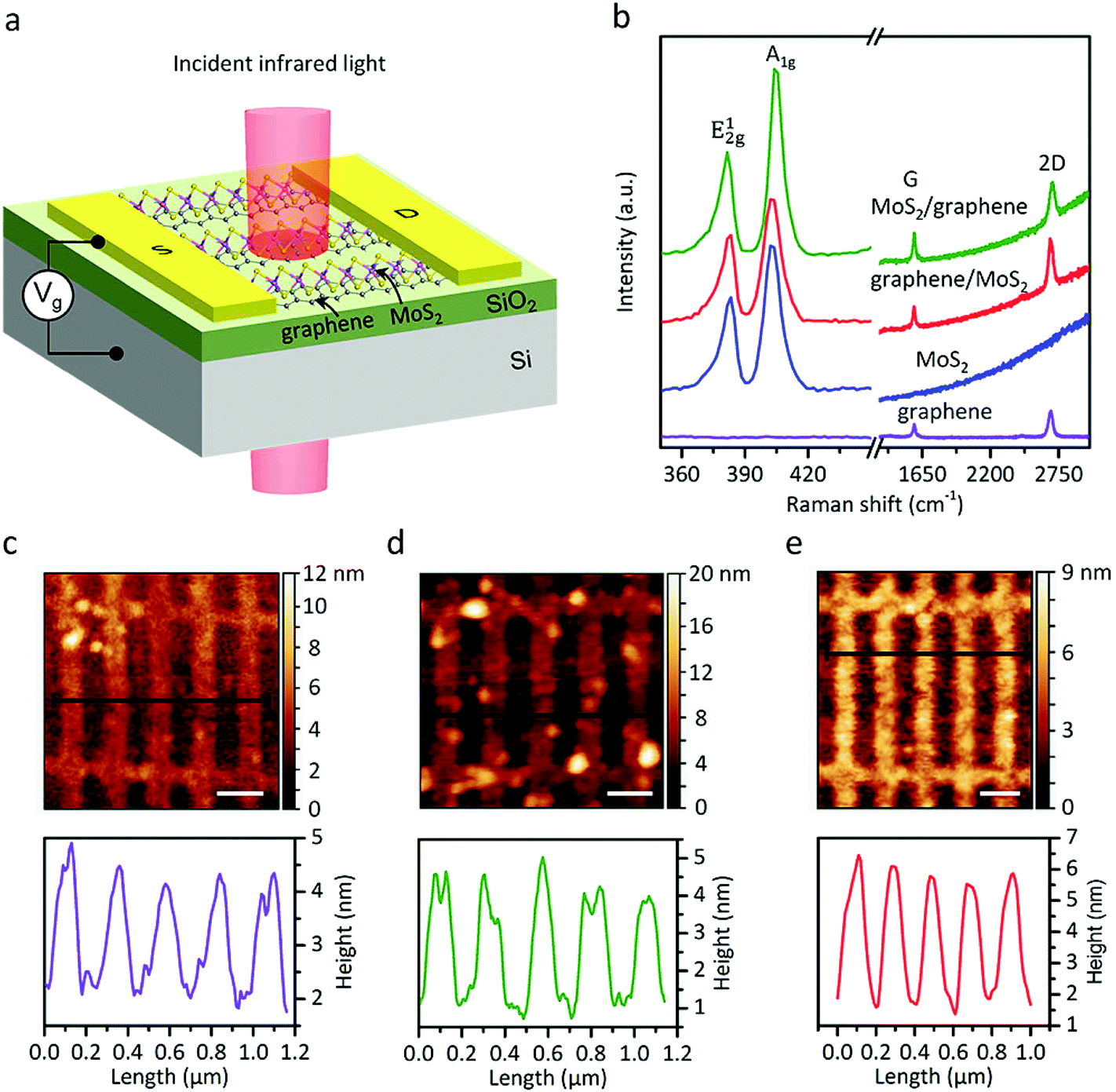 | ||
Fig. 1 (a) FTIR measurement scheme for electrically tunable graphene and MoS2 heterostructures. Here, the MoS2/graphene nanoribbon array is used as an example. (b) Raman spectra of MoS2/graphene, graphene/MoS2, MoS2, and graphene on an SiO2/Si substrate, obtained using a 514 nm excitation wavelength. (c, d, e) Top: AFM image of the graphene, MoS2/graphene, and graphene/MoS2 devices (scale bar = 200 nm). Bottom: line-scan profile of the top image, corresponding to the black line. The ribbon width (W) is 100 nm and the width to pitch ratio is 1![[thin space (1/6-em)]](https://www.rsc.org/images/entities/char_2009.gif) :1. The thicknesses of the graphene, MoS2/graphene, and graphene/MoS2 nanoribbons are about 2.1 nm, 3.1 nm, and 4.0 nm, respectively. :1. The thicknesses of the graphene, MoS2/graphene, and graphene/MoS2 nanoribbons are about 2.1 nm, 3.1 nm, and 4.0 nm, respectively. | ||
The MoS2, graphene, MoS2/graphene, and graphene/MoS2 films were patterned into electrically continuous nanoribbon arrays with a 1:1 width-to-pitch ratio. The ribbon widths were characterized by atomic force microscopy (AFM) (Fig. 1c–e and S1b in the ESI†) to be 100 nm, with the graphene, MoS2, MoS2/graphene, and graphene/MoS2 nanoribbons possessing a uniform thickness of ca. 2.1 nm, 1.9 nm, 3.1 nm, and 4.0 nm, respectively. These values are larger than the thickness of a single layer of graphene (0.35 nm (ref. 25)) and MoS2 (0.6 nm (ref. 26)), which may be attributed to residual poly(methyl methacrylate) (PMMA) on the graphene during the transfer process and partial etching of the SiO2 substrate in the O2 plasma etching process.Ti/Au (5 nm/60 nm) metal stacks were deposited as the source and drain electrodes (an optical microscope image of the device can be viewed in Fig. S1a in the ESI†). A titanium buffer layer was used to form an Ohmic contact with the MoS2 or graphene layer and to increase the adhesion force of the Au electrodes. The tunneling barrier height was zero between the Ti and MoS2 under the electrodes, due to the metallic behavior of the Ti–MoS2 system.27 P+ doped Si beneath the 300 nm SiO2 layer was used as a back gate electrode. The Isd–Vsd curves measured from the bare graphene and MoS2 devices both exhibit a linear relationship (Fig. S2 in the ESI†), confirming the formation of an Ohmic contact.
Electrical measurements
All electrical measurements were performed using a semiconductor parameter analyzer under ambient conditions. The transport properties of the bare MoS2 devices were evaluated and a transfer curve (Isd–Vg) at Vsd = 100 meV is shown in Fig. 2a. The device was observed to possess an n-doped behavior with a minimum Isd at Vg = −37 V, which may be attributed to S vacancies.28 The carrier mobility of the MoS2 device was calculated to be ca. 13 cm2 (V s)−1, which is comparable to previously reported values.29,30 When Vg = 0 V, the calculated electron density and Fermi level in MoS2 was 2.77 × 1012 cm−2 and 9.5 meV, respectively (see calculation of carrier density, Fermi level, and mobility in the ESI†). | ||
| Fig. 2 (a) Transfer characteristics of a MoS2 device. Inset: Enlarged view of the minimum current obtained at Vg = −37 V. (b) Transfer characteristics of the graphene, MoS2/graphene, and graphene/MoS2 devices. The light red strip indicates the increase in Isd of electron branch with the variation of gate voltage is extremely slow compared to its dramatic decrease of hole branch for the graphene/MoS2 device. (c) Schematic band diagram of the MoS2/graphene device with Ti metal in the isolated state. (d) Schematic band diagram after graphene contact with MoS2 without applying an electric field. | ||
The transfer curves of the graphene, MoS2/graphene and graphene/MoS2 nanoribbon devices are shown in Fig. 2b. Three key trends can be identified in these curves. Firstly, the Isd values of the MoS2/graphene and graphene/MoS2 devices are in the same order of magnitude as those of the bare graphene device, but are two orders of magnitude larger than those of the MoS2 device, suggesting that transport is mainly graphene controlled. Secondly, the VCNP (at ca. 50 V) value for the graphene/MoS2 device was considerably smaller than for the graphene and the MoS2/graphene devices (not observed in the region less than 100 V). Graphene is heavily p-doped here, which may be due to residual PMMA and H2O molecules31 or surface dangling bonds on the SiO2 substrate.32 Once the graphene was brought into contact with the MoS2, electrons transferred from the MoS2 to the graphene, as the work function of MoS2 is smaller than that of graphene (as displayed in Fig. 2c). This process weakens the p-doping effect in the graphene and leads to the formation of a Schottky barrier at the interface in the absence of a gate voltage (Vg) (Fig. 2d). MoS2 beneath the graphene can further reduce the p-doping from the SiO2 substrate. Thus, the VCNP value of the graphene/MoS2 device is the lowest among the three systems. Thirdly, the electron branch of the transfer curve of the graphene/MoS2 device is very different from those of the graphene and MoS2/graphene devices.33,34 As shown, the increase in Isd for the graphene/MoS2 device is extremely slow and reaches saturation when Vg approaches 100 V. This result is attributed to the lower mobility of electrons in MoS2 compared to graphene and also the band arrangement in the graphene/MoS2 heterostructure, which is induced by a sufficiently large positive gate voltage.18 Once the Fermi level of graphene is higher than the MoS2 conduction band edge, gate-induced electrons in graphene can easily transfer to MoS2 without a barrier, resulting in an electron increase in MoS2 and an electron decrease in graphene.
Plasmons in graphene–MoS2 heterostructures
The graphene plasmons in the heterostructures were measured by Fourier transform infrared (FTIR) microscopy, as shown in Fig. 1a. Graphene layers were etched into nanoribbon arrays to excite the plasmons. A single-beam transmittance spectrum collected at the charge neutral point (TCNP) was used as the background spectrum and the single-beam transmittance spectrum (T) at each Fermi level was measured to obtain the extinction spectrum using the equation 1 − T/TCNP.35–37 Each measurement was repeated three times to confirm the extinction spectra. The extinction spectra of the as-prepared MoS2/graphene, and graphene/MoS2 devices are plotted in Fig. 3a and b, respectively. As a comparison, Fig. 3c shows the extinction spectra of the bare graphene nanoribbon array. There are three peaks in all of these extinction spectra (denoted peak 1, peak 2, and peak 3), which originate from hybridization between the graphene plasmon and two surface optical phonons of the SiO2 substrate, denoted as SO1 (806 cm−1) and SO2 (1168 cm−1).38 The small features observed between 1000 cm−1 and 1200 cm−1 in the extinction spectra may be attributed to the rapidly varying dynamic dielectric function of the SiO2 substrate,38 and the change in the graphene Fermi level. These peaks were also observed in the IR absorption spectra of the SiO2/Si substrate covered by the graphene film with a varying Fermi level (Fig. S3 in the ESI†). | ||
| Fig. 3 (a, b, c) Extinction spectra of the MoS2/graphene, graphene/MoS2, and graphene nanoribbon array devices on SiO2 measured at varying gate bias ΔCNP, ΔCNP = Vg − VCNP. Ribbon width (W): 100 nm. (d, e, f) Simulated extinction spectra of MoS2/graphene, graphene/MoS2, and graphene nanoribbon array devices on SiO2. The corresponding |EF| is shown above each curve. The simulation results match well with our experiment data. Extinction curves with the same color were measured at equivalent gate bias values. SO1 and SO2 represent the two surface optical phonons of SiO2 at 806 cm−1 and 1168 cm−1, respectively. The small peaks between 1000 cm−1 and 1200 cm−1 may be attributed to the rapidly varying dynamic dielectric function of the SiO2 substrate in this region. | ||
As shown in Fig. 3a–c, plasmons in the heterostructures of graphene and monolayer MoS2 exhibit similar properties to those in bare graphene. Monolayer MoS2 does not introduce new peaks into the extinction spectra in our detection region (from 675 cm−1 to 4000 cm−1), because there are no IR-active phonons nor any plasmon resonance in this region.39,40 Control experiments of the bare MoS2 device and the MoS2 film/graphene device further prove that there is no resonance absorption for MoS2, as shown in Fig. S4 in the ESI.† This may be attributed to the low electron concentration (1012–1013 cm−2) of MoS2 in our experiments. Theoretical studies indicate that plasmon resonances of two-dimensional MoS2 with a carrier concentration of 1012–1014 cm−2 appear in the far-infrared and terahertz regimes.39
The electrical tunability of graphene plasmons remained in the heterostructures of graphene and monolayer MoS2. As displayed in Fig. 3a and b, three resonance peaks shift to blue as |ΔCNP| increases due to the increased charge density. We extracted the value of all of these resonance peaks at each gate voltage and plotted them as a function of ΔCNP in Fig. 4a. From this figure, the tunability of plasmons in the heterostructures is obviously shown. Although the main features of the plasmons in the heterostructures remain, the introduction of monolayer MoS2 induced frequency and intensity changes in the resonance peaks. Compared with bare graphene devices, the resonance peaks of both the MoS2/graphene and graphene/MoS2 devices exhibit a redshift, as shown in Fig. 4a. For instance, when ΔCNP = −120 V, peak 1, peak 2, and peak 3 of the MoS2/graphene device redshift by 43 cm−1, 88 cm−1, and 125 cm−1, and the peaks of the graphene/MoS2 device redshift by 65 cm−1, 111 cm−1, and 133 cm−1 compared to the frequencies of the bare graphene device at 814 cm−1, 954 cm−1, and 1382 cm−1. Furthermore, the peak intensities of the heterostructures are weaker than that of the bare graphene device. For example, when ΔCNP = −120 V, the highest peak intensities for the graphene, MoS2/graphene, and graphene/MoS2 devices were 0.73%, 0.48%, and 0.23%, respectively.
 | ||
| Fig. 4 (a) The dependence of the resonance frequency of graphene (violet), MoS2/graphene (green), and graphene/MoS2 (red) on the gate bias |ΔCNP|. For graphene/MoS2, the resonance was too weak to identify the peak positions at |ΔCNP| = 50 V, so the peak positions are not shown here. The two gray dashed lines show the positions of the SO1 and SO2 phonons of the SiO2 substrate. (b) The calculated effective voltage on graphene for the bare graphene (violet), MoS2/graphene (green), and graphene/MoS2 (red) devices at varying gate bias |ΔCNP|. | ||
The frequency redshift and strength reduction of plasmons in the heterostructures of graphene and monolayer MoS2 are due to changes in the environmental dielectric and the effective Fermi level of graphene, according to the equation:9,41,42 , where e is the electron charge, EF is the Fermi level of graphene, q is the wave vector which can be determined by the ribbon width W via q = π/W, ℏ is the reduced Planck constant, ε0 is the vacuum permittivity of free space, and εr is the average dielectric constant of the environment around graphene. Here, for all the devices, W = 100 nm, which means that the value of q is fixed at a value of 3.14 × 105 cm−1. Thus, the resonance frequency is determined by two variables: EF and εr of graphene. The εr value of the graphene/SiO2 devices is
  , where εair = 1, and εSiO2 = 3.9.43 Because the reported static relative permittivity for single-layer MoS2 is εSL−MoS2 = 3.7,44 which is slightly smaller than that of SiO2 and much larger than εair, the εr value for the graphene/MoS2 device is slightly smaller than εr(G/SiO2), and the εr value for the MoS2/graphene device is large than εr(G/SiO2). However, the resonance frequencies of the bare graphene devices are much higher than those of the two heterostructured devices, and the frequencies of the graphene/MoS2 devices are lower than those of the MoS2/graphene devices at every ΔCNP value (Fig. 4a). These results indicate that the EF of graphene in the graphene/MoS2 device is the lowest at the same value of ΔCNP. The EF value in the bare graphene device was calculated using a parallel plate capacitor model (details in ESI†), as marked in Fig. 3f.
The plasmonic behavior of the MoS2/graphene, graphene/MoS2 and bare graphene devices were also studied via a finite element method. The simulated results corresponding to Fig. 3a–c are shown in Fig. 3d–f. An effective electrical ribbon width of 68 nm (ref. 37) and a width-to-pitch ratio of 1:2 was used for all of the devices (see more details of the simulation method in the ESI†). For the bare graphene devices, the calculated EF values were used in the simulation and the obtained simulated curves (Fig. 3f) were found to be in good agreement with experimental results (Fig. 3c). For the heterostructured devices, the EF value of graphene was used as a variable in the simulation and was adjusted to get the best fitting curves (the EF values used are shown in Fig. 3d and e). The resonance frequencies of each of the three peaks correspond closely to their experimental values and their resonance intensities were also in good agreement with the experimental values. The resonance intensities of the bare graphene devices were found to be approximately 2 times that of the MoS2/graphene devices and 4 times that of the graphene/MoS2 devices. The plasmon resonance intensity of graphene is closely related to its EF value, with large |EF| values tending to indicate a strong resonance intensity.45,46 Thus, the simulation results indicate that the graphene plasmon keeps its main features in the heterostructures of graphene and monolayer MoS2 while the effective EF and εr values determine its resonance frequency and intensity.
From the obtained |EF| values, we calculated the effective gate voltage of graphene at certain |ΔCNP| values in the heterostructures, as plotted in Fig. 4b. In the heterostructures, only part of the applied gate voltage works on the graphene layer due to screening and charge transfer between monolayer MoS2. Ignoring the carrier transfer between graphene and MoS2, we roughly estimated the carrier distribution in each layer of the graphene–MoS2 heterostructures via Thomas–Fermi (T–F) charge screening theory. Details can be found in the ESI.† The utilised charge screening lengths of graphene and MoS2 were λgraphene = 0.6 nm and λMoS2 = 7 nm.25,47 The calculated carrier density of graphene in the MoS2/graphene and graphene/MoS2 devices was ca. 73% and ca. 48% of that in the bare graphene device, respectively. This evaluation exhibited a similar tendency to previous results. The deviation between the exact values may arise from carrier transfer between graphene, and impurities, and the simplification of the T–F model for a two-atom thick layered heterostructure. We want to clarify that, due to its large screening length and ultra-thin thickness, the screening effect is much weaker than in bulk semiconductors, which may totally screen the gate electric field.
The lifetime of the plasmon, T, can be extracted from the infrared extinction spectra using the equation T = 2ħ/Γ, where Γ is the full width at half-maximum (FWHM) of the resonance peaks.48 Due to plasmon–phonon coupling with the SiO2 phonons, which can be described with the electromagnetic induced transparent (EIT) model or the Fano model, the Γ value of the plasmon resonance in the MoS2/graphene and graphene/MoS2 heterostructures were obtained via curve fitting.35 The details can be found in Fig. S5 in the ESI.† The calculated lifetimes for the MoS2/graphene devices are between 80 fs and 100 fs, and for the graphene/MoS2 devices are about 80 fs. These values are comparable with previously reported values for graphene/SiO2 devices in the same frequency range.35 This suggests that the monolayer MoS2 causes little loss to plasmons in the graphene and MoS2 heterostructures, which is beneficial for the support of plasmons with high performance in optoelectronic integrated devices. This is another advantage of MoS2 compared to bulk semiconductors for graphene plasmons.
Finally, we want to discuss the electron plasmons in the graphene/MoS2 heterostructure. The electrical tunability of the Fermi energy of the graphene device with the back gate is symmetric with respect to the CNP,33 however, it is asymmetric for graphene/MoS2. We measured the hole plasmons and the electron plasmons at both sides of the CNP of the graphene/MoS2 devices (Fig. 5a). The results show that the hole plasmons are distinct. However, the electron plasmons were not detectable, even at very high ΔCNP values (80 V). This phenomenon is consistent with the electrical properties of the graphene/MoS2 device, as proven by its transfer characteristics (the red line in Fig. 2b), where the Ids value nearly does not increase with Vg in the n-doped region. When the back gate voltage, Vg, is applied, it causes bending in the bottom-layer MoS2 conduction band (Fig. 5b). When the positive Vg exceeds a critical gate voltage, the EF of graphene becomes higher than the MoS2 conduction band edge, and thus gate-induced electrons in graphene are able to transfer to MoS2 without a barrier. This results in the electrons in MoS2 increasing dramatically and a reduction in the electron density in graphene (Fig. 5b), which is called the negative compressibility of the MoS2 electron system.18 Meanwhile, the contact between graphene and MoS2 transforms from a Schottky barrier into an Ohmic contact. Based on this property, we suggest a new kind of plasmonic structure based on the graphene/MoS2 heterostructure, where graphene is kept as a complete plane to keep its high quality and nanostructures are designed using MoS2.
 | ||
| Fig. 5 (a) The hole and electron extinction spectra of the graphene/MoS2 nanoribbon device at varying negative and positive ΔCNP values. The VCNP of the graphene/MoS2 device was 50 V. The ribbon width (W) was 100 nm. (b) Schematic band arrangement of graphene/MoS2 on SiO2 with an applied Vg. Left: Negative Vg is applied. Right: Positive Vg is applied. The red dashed lines show the positions of EF. The black dots represent electrons, and the black line with an arrow means that the electrons transfer from graphene to MoS2. | ||
Conclusions
The effects of semiconducting MoS2 on graphene plasmons are studied in heterostructures of graphene and monolayer MoS2 with different stacking sequences under a back gate. Our measurements show that monolayer MoS2 induces quite little deterioration on the plasmon lifetime but there is charge transfer between graphene and MoS2. At equivalent ΔCNP voltages, the resonance frequencies of the graphene/MoS2 devices are lower than that of MoS2/graphene, and they both are lower than that of the bare graphene device. The redshift and weakening of the resonance are mainly determined by the lower doping of graphene in the heterostructures due to the electrical screening effect. Due to the electron transfer from graphene to MoS2 at Vg values larger than the critical value, electron plasmons are totally cancelled in graphene/MoS2 devices with a back gate. We suggest that this property can be used to achieve high quality electron plasmons in whole graphene by designing MoS2 nanostructures to avoid edge scattering in graphene nanostructures. These findings demonstrate electrically tunable graphene plasmons in contact with a monolayer semiconductor, and suggest that van der Waals heterostructures are very promising candidates to integrate high quality electronic and optoelectronic devices on a chip.Experimental section
Graphene was grown on copper foil at 1050 °C with a mixture of methane and hydrogen using the CVD technique.21 Monolayer MoS2 was grown on a sapphire substrate using sulfur and MoO3 as a solid source through an oxygen-assisted CVD method.20 Taking the fabrication of the MoS2/graphene device as an example, graphene sheets were transferred from copper foil using a standard wet method.21 PMMA (MicroChem) was spun cast onto the graphene/Cu foils for 1 min, and baked at 180 °C for 2 min. Then, the PMMA/graphene/Cu foils were floated on the surface of a ferric chloride solution for several hours to remove the Cu. After the Cu was dissolved, the PMMA/graphene films were “pulled” out of the solution using the SiO2/Si substrates, and placed in hot acetone for 40 min to remove the PMMA. MoS2 films were removed from the sapphire substrates following a similar method with the only difference being that the sapphire substrates were etched in an aqueous solution of sodium hydroxide for several hours. Due to the excellent visibility of the graphene and MoS2 films on the 300 nm SiO2/Si substrates with the naked eye, it is easy to stack MoS2 onto the graphene sheets in the “pull” step. Next, nanoribbon arrays were patterned in graphene covered by MoS2 and uncovered regions using 100 keV electron-beam lithography (EBL) (Vistec 5000+ES, Germany) on approximately 260 nm of PMMA, followed by oxygen plasma etching at 5 Pa and 100 W for 10 s. The source and drain electrodes of the device were defined on the PMMA in a second lithography step, followed by an e-beam evaporation of 5 nm of Ti and 60 nm of Au. A lift-off process was then performed by immersing the devices in hot acetone. All device fabrication processes were performed in a clean room environment.Raman spectra were taken with a Horiba Jobin Yvon LabRAM HR800 microscope. The electrical transport properties were analyzed using a semiconductor parameter analyzer (Keithley 4200-SCS), which was equipped with three wolframium probes. AFM measurements were conducted using a scattering SNOM (Neaspec GmbH). Infrared transmission measurements were performed by FTIR microscopy (Thermo Fisher Nicolet iN10). All characterization of the devices’ performance was conducted under ambient conditions.
Acknowledgements
This work was supported by the National Basic Research Program of China (Grant No. 2015CB932400, 2016YFA0201600), the National Natural Science Foundation of China (Grant No. 51372045, 11504063), the Bureau of International Cooperation, Chinese Academy of Sciences (121D11KYSB20130013), and the key program of the bureau of Frontier Sciences and Education Chinese Academy of Sciences (QYZDB-SSW-SLH021).Notes and references
- M. J. Kobrinsky, et al. , Intel Technol. J., 2004, 8, 129 Search PubMed.
- E. Ozbay, Science, 2006, 311, 189 CrossRef CAS PubMed.
- V. J. Sorger, R. F. Oulton, R. M. Ma and X. Zhang, MRS Bull., 2012, 37, 728 CrossRef CAS.
- W. L. Barnes, A. Dereux and T. W. Ebbesen, Nature, 2003, 424, 824 CrossRef CAS PubMed.
- S. I. Bozhevolnyi, V. S. Volkov, E. Devaux, J. Y. Laluet and T. W. Ebbesen, Nature, 2006, 440, 508 CrossRef CAS PubMed.
- A. Y. Nikitin, F. Guinea, F. J. Garcia-Vidal and L. Martin-Moreno, Phys. Rev. B: Condens. Matter, 2011, 84, 161407 CrossRef.
- A. Woessner, M. B. Lundeberg, Y. Gao, A. Principi, P. Alonso-Gonzaolez, M. Carrega, K. Watanabe, T. Taniguchi, G. Vignale, M. Polini, J. Hone, R. Hillenbrand and F. H. L. Koppens, Nat. Mater., 2015, 14, 421 CrossRef CAS PubMed.
- J. Chen, M. Badioli, P. Alonso-Gonzalez, S. Thongrattanasiri, F. Huth, J. Osmond, M. Spasenovic, A. Centeno, A. Pesquera, P. Godignon, A. Zurutuza Elorza, N. Camara, F. Javier Garcia de Abajo, R. Hillenbrand and F. H. L. Koppens, Nature, 2012, 487, 77 CrossRef CAS PubMed.
- A. N. Grigorenko, M. Polini and K. S. Novoselov, Nat. Photonics, 2012, 6, 749 CrossRef CAS.
- F. J. Garcia de Abajo, ACS Photonics, 2014, 1, 135 CrossRef CAS.
- T. Low and P. Avouris, ACS Nano, 2014, 8, 1086 CrossRef CAS PubMed.
- Y.-J. Yu, Y. Zhao, S. Ryu, L. E. Brus, K. S. Kim and P. Kim, Nano Lett., 2009, 9, 3430 CrossRef CAS PubMed.
- T. Roy, M. Tosun, J. S. Kang, A. B. Sachid, S. B. Desai, M. Hettick, C. C. Hu and A. Javey, ACS Nano, 2014, 8, 6259 CrossRef CAS PubMed.
- D. Qu, X. Liu, F. Ahmed, D. Lee and W. J. Yoo, Nanoscale, 2015, 7, 19273 RSC.
- L. Yu, Y. H. Lee, X. Ling, E. J. Santos, Y. C. Shin, Y. Lin, M. Dubey, E. Kaxiras, J. Kong, H. Wang and T. Palacios, Nano Lett., 2014, 14, 3055 CrossRef CAS PubMed.
- S. A. Maier, Plasmonics: Fundamentals and Applications, Springer-Verlag, New York, 2007 Search PubMed.
- H. Hu, F. Zhai, D. Hu, Z. Li, B. Bai, X. Yang and Q. Dai, Nanoscale, 2015, 7, 19493 RSC.
- S. Larentis, J. R. Tolsma, B. Fallahazad, D. C. Dillen, K. Kim, A. H. MacDonald and E. Tutuc, Nano Lett., 2014, 14, 2039 CrossRef CAS PubMed.
- J. Meng, H.-D. Song, C.-Z. Li, Y. Jin, L. Tang, D. Liu, Z.-M. Liao, F. Xiu and D.-P. Yu, Nanoscale, 2015, 7, 11611 RSC.
- W. Chen, J. Zhao, J. Zhang, L. Gu, Z. Yang, X. Li, H. Yu, X. Zhu, R. Yang, D. Shi, X. Lin, J. Guo, X. Bai and G. Zhang, J. Am. Chem. Soc., 2015, 137, 15632 CrossRef CAS PubMed.
- X. Li, W. Cai, J. An, S. Kim, J. Nah, D. Yang, R. Piner, A. Velamakanni, I. Jung, E. Tutuc, S. K. Banerjee, L. Colombo and R. S. Ruoff, Science, 2009, 324, 1312 CrossRef CAS PubMed.
- C. Lee, H. Yan, L. E. Brus, T. F. Heinz, J. Hone and S. Ryu, ACS Nano, 2010, 4, 2695 CrossRef CAS PubMed.
- S.-L. Li, H. Miyazaki, H. Song, H. Kuramochi, S. Nakaharai and K. Tsukagoshi, ACS Nano, 2012, 6, 7381 CrossRef PubMed.
- A. C. Ferrari, J. C. Meyer, V. Scardaci, C. Casiraghi, M. Lazzeri, F. Mauri, S. Piscanec, D. Jiang, K. S. Novoselov, S. Roth and A. K. Geim, Phys. Rev. Lett., 2006, 97, 187401 CrossRef CAS PubMed.
- Y. Sui and J. Appenzeller, Nano Lett., 2009, 9, 2973–2977 CrossRef CAS PubMed.
- A. Splendiani, L. Sun, Y. Zhang, T. Li, J. Kim, C. Y. Chim, G. Galli and F. Wang, Nano Lett., 2010, 10, 1271 CrossRef CAS PubMed.
- W. Liu, D. Sarkar, J. Kang, W. Cao and K. Banerjee, ACS Nano, 2015, 9, 7904 CrossRef CAS PubMed.
- S. McDonnell, R. Addou, C. Buie, R. M. Wallace and C. L. Hinkle, ACS Nano, 2014, 8, 2880 CrossRef CAS PubMed.
- M. S. Fuhrer and J. Hone, Nat. Nanotechnol., 2013, 8, 146 CrossRef CAS PubMed.
- B. Radisavljevic and A. Kis, Nat. Mater., 2013, 12, 815 CrossRef CAS PubMed.
- N. Jain, T. Bansal, C. Durcan and B. Yu, IEEE Electron Device Lett., 2012, 33, 925 CrossRef CAS.
- Y. Shi, X. Dong, P. Chen, J. Wang and L.-J. Li, Phys. Rev. B: Condens. Matter, 2009, 79, 115402 CrossRef.
- K. S. Novoselov, A. K. Geim, S. V. Morozov, D. Jiang, Y. Zhang, S. V. Dubonos, I. V. Grigorieva and A. A. Firsov, Science, 2004, 306, 666 CrossRef CAS PubMed.
- C. J. Shih, Q. H. Wang, Y. Son, Z. Jin, D. Blankschtein and M. S. Strano, ACS Nano, 2014, 8, 5790 CrossRef CAS PubMed.
- X. Yang, F. Zhai, H. Hu, D. Hu, R. Liu, S. Zhang, M. Sun, Z. Sun, J. Chen and Q. Dai, Adv. Mater., 2016, 28, 2931–2938 CrossRef CAS PubMed.
- H. Hu, X. Yang, F. Zhai, D. Hu, R. Liu, K. Liu, Z. Sun and Q. Dai, Nat. Commun., 2016, 7, 12334 CrossRef CAS PubMed.
- H. Yan, T. Low, W. Zhu, Y. Wu, M. Freitag, X. Li, F. Guinea, P. Avouris and F. Xia, Nat. Photonics, 2013, 7, 394–399 CrossRef CAS.
- A. Kucirkova and K. Navratil, Appl. Spectrosc., 1994, 48, 113 CrossRef CAS.
- A. Scholz, T. Stauber and J. Schliemann, Phys. Rev. B: Condens. Matter, 2013, 88, 035135 CrossRef.
- Y. Wang, J. Z. Ou, A. F. Chrimes, B. J. Carey, T. Daeneke, M. M. Alsaif, M. Mortazavi, S. Zhuiykov, N. Medhekar, M. Bhaskaran, J. R. Friend, M. S. Strano and K. Kalantar-Zadeh, Nano Lett., 2015, 15, 883 CrossRef CAS PubMed.
- S. H. Abedinpour, G. Vignale, A. Principi, M. Polini, W.-K. Tse and A. H. MacDonald, Phys. Rev. B: Condens. Matter, 2011, 84, 045429 CrossRef.
- S. Badhwar, J. Sibik, P. R. Kidambi, H. E. Beere, J. A. Zeitler, S. Hofmann and D. A. Ritchie, Appl. Phys. Lett., 2013, 103, 121110 CrossRef.
- H. L. Xu, Z. Y. Zhang, H. T. Xu, Z. X. Wang, S. Wang and L. M. Peng, ACS Nano, 2011, 5, 5031 CrossRef CAS PubMed.
- D. Davelou, G. Kopidakis, G. Kioseoglou and I. N. Remediakis, Solid State Commun., 2014, 192, 42 CrossRef CAS.
- L. Ju, B. S. Geng, J. Horng, C. Girit, M. Martin, Z. Hao, H. A. Bechtel, X. G. Liang, A. Zettl, Y. R. Shen and F. Wang, Nat. Nanotechnol., 2011, 6, 630 CrossRef CAS PubMed.
- Y. Zhao, G. X. Chen, Z. C. Tao, C. Y. Zhang and Y. W. Zhu, RSC Adv., 2014, 4, 26535 RSC.
- S. Das and J. Appenzeller, Nano Lett., 2013, 13, 3396 CrossRef CAS PubMed.
- C. Sonnichsen, T. Franzl, T. Wilk, G. von Plessen, J. Feldmann, O. Wilson and P. Mulvaney, Phys. Rev. Lett., 2002, 88, 077402 CrossRef CAS PubMed.
Footnote |
| † Electronic supplementary information (ESI) available. See DOI: 10.1039/c6nr07081g |
| This journal is © The Royal Society of Chemistry 2017 |