
Influence of solution- and thermal-annealing processes on the sub-nanometer-ordered organic–organic interface structure of organic light-emitting devices†
S.
Ohisa
a,
Y.-J.
Pu
*a,
N. L.
Yamada
b,
G.
Matsuba
a and
J.
Kido
*a
aDepartment of Organic Materials Science, Graduate School of Organic Materials Science, Yamagata University, Yonezawa, Yamagata, 992-8510 Japan. E-mail: pu@yz.yamagata-u.ac.jp; kid@yz.yamagata-u.ac.jp
bInstitute of Material Structure Science, High-Energy Accelerator Research Organization (KEK), 203-1 Shirakata, Tokai, Naka 319-1106, Japan
First published on 31st October 2016
Abstract
Solution- and thermal-annealing processed organic–organic interface structures were investigated by neutron reflectometry. We revealed the true picture of interfaces, a polymer hole-transporting layer – a small molecule light-emitting layer – a small molecule electron-transporting layer, and discussed influences of those interface structures on organic light-emitting devices.
The performance of solution-processed organic light-emitting devices (OLEDs)1–6 currently lags that of conventional evaporation-processed devices.7–10 A major reason for this is the difficulty associated with forming multilayer structures via solution processing. In evaporation-processed OLEDs, each optoelectronic function is separated into a different layer, including a hole-injection layer, a hole-transporting layer (HTL), a light-emitting layer (EML), an electron-transporting layer (ETL), and an electron-injection layer. Appropriate device design based on such function separation has advanced the device performance of evaporation-processed OLEDs. However, in the case of solution-processed OLEDs, multilayer design is difficult because upperlayer coating solvents can dissolve and rinse away underlayers during the upperlayer coating process. To obtain multilayer structures, strict solvent selection is required to avoid dissolution of the underlayer molecules. Layer stacking on a small-molecule layer is particularly difficult because of the intrinsically high solubility of small molecules.
Recently, proper molecular design and solvent selection have enabled ETL stacking on small-molecule EMLs via a solution process.1,4,6 Aizawa et al. comprehensively investigated the resistance of various small carbazole-type host molecules to several alcohol solvents used for processing upperlayer ETLs and found that even small molecules can exhibit sufficient resistance to the alcohols. Using the constructed multilayer structure, they achieved record-high power efficiencies in solution-processed OLEDs. Precise evaluation and design of solution-processed organic–organic interface structures is essential to achieve an even higher performance. Aizawa et al. investigated the formed interfaces using secondary-ion mass spectrometry (SIMS), which is a general interface analysis method. However, SIMS cannot provide a true picture of interface structures because of its resolution lack in the vertical direction and its destructive nature.
Neutron reflectometry (NR) is a nondestructive and highly quantitative analytical method that enables precise evaluation of interface structures with sub-nanometer-order resolution.11–19 In NR, deuteration of samples substantially increases the scattering length densities (SLDs) within layers, which enhances SLD contrast to an adjacent nondeuterated compound layer and enables analysis of the interface structure between the two organic layers. Here, deuteration minimally affects the physical and chemical properties of the original nondeuterated compounds.
The literature contains various reports of analyses of solution-processed polymer/small-molecule interfaces by NR.11,14–16,18 Burn et al. used NR to investigate the effect of solution and thermal-annealing processes on the interfaces between p-type π-conjugated polymers and fullerene derivatives in organic photovoltaic cells;11,18 they observed that the fullerene derivatives diffused into the p-type π-conjugated polymers. In our previous work, we observed the diffusion of compounds at the interface between a polymer HTL, poly[N,N′-bis(4-butylphenyl)-N,N′-bis(phenyl)-benzidine] (PTPD), and a small-molecule EML, tris-(2-(4-methylphenyl)pyridine)iridium(III) (Ir(mppy)3)-doped 3,3′-[bis(9,9′-phenylcarbazol-3-yl)]-benzophenone (BCzBP) (or deuterated BCzBP (BCzBP-d14)), in OLEDs by NR and fluorescence resonance energy transfer (FRET) analyses; we also investigated the influence of interface structures on OLED characteristics.16 However, to the best of our knowledge, the literature contains no reports involving analyses of solution-processed small-molecule/small-molecule interfaces in OLEDs. Solution processing mainly comprises two steps: a coating process to form a film and a thermal-annealing process to dry the film. Therefore, interface analysis by NR should consider the effect of these two processes.
In this work, we succeeded in precisely evaluating a solution-processed small-molecule EML/small-molecule ETL interface in OLEDs using NR and FRET analyses. We used Ir(mppy)3-doped BCzBP (or BCzBP-d14) as the EML and 1,3,5-tris(1-phenyl-1H-benzimidazol-2-yl)benzene (TPBi) as the ETL. The EML/evaporated TPBi bilayer film exhibited a sharp interface, whereas the EML/solution-processed TPBi bilayer film exhibited a largely interdiffused interface. Thermal diffusion at the interfaces was also investigated. Asymmetric thermal diffusion was observed because of the differences in the glass-transition temperatures (Tgs) of the different compounds. Further, we found that the interface structure of trilayer films, which consisted of PTPD as the HTL, Ir(mppy)3-doped BCzBP (or BCzBP-d14) as the EML, and TPBi as the ETL, exhibited a more precise interface structure than the bilayer films. Finally, we fabricated OLEDs with several types of interfaces and investigated the influence of the interface structures on the device characteristics.
The chemical structures of the compounds are shown in Fig. S1.† Ir(mppy)3 was used as an emitter, and BCzBP (or BCzBP-d14) was used as the host compound in the EML. TPBi was used as the ETL, and PTPD was used as the HTL. The characteristics of the materials are described in the ESI (Table S1 and Fig. S2†). The solution-processed and evaporated EML with BCzBP (or BCzBP-d14) are abbreviated as sEML and eEML, respectively. The solution-processed and evaporated ETLs are abbreviated as sTPBi and eTPBi, respectively.
Before investigating the multilayer films by NR, we evaluated the single-layer films because the multilayer films were analyzed on the basis of the results for the single-layer films. The thicknesses and SLD values of the single-layer films obtained by NR are shown in Fig. S3 and Table S2.† We next fabricated the bilayer films consisting of an EML and an ETL. BCzBP-d14:9 wt% Ir(mppy)3 (sEML) was spin coated onto a Si wafer and annealed; TPBi was subsequently spin coated onto the sEML film, and the resulting bilayer film [sEML/sTPBi] was annealed at 115 °C. The spin-coating conditions for sEML and sTPBi were the same as those used for the single-layer films in the preliminary experiments. TPBi was also evaporated (as eTPBi) onto sEML films to form [sEML/eTPBi] for comparison with [sEML/sTPBi].
The NR profile of the [sEML/eTPBi] film was well reproduced using a two-organic-layer model (Fig. 1). The thicknesses and SLDs of the sEML and eTPBi layers in [sEML/eTPBi] were the same as those of each corresponding single-layer film. This result indicates that the interface of [sEML/eTPBi] is extremely sharp and that the molecules in sEML and eTPBi did not diffuse into the opposing layer. The NR profile of the [sEML/sTPBi] film was also reproduced using a two-organic-layer model; however, large interdiffusion was observed in the [sEML/sTPBi] film. The SLD of sEML in [sEML/sTPBi] was smaller than that of the corresponding single-layer film, indicating that TPBi, with an SLD lower than that of sEML itself, diffused. The SLD of sTPBi in [sEML/sTPBi] was larger than that of the corresponding single-layer film, also indicating the diffusion of an EML with a higher SLD than that of sTPBi itself. The volume ratios of TPBi in the mixed sEML and sEML molecules in the mixed sTPBi were estimated to be 21% and 22%, respectively, on the basis of the SLD values. Details of the volume ratio estimation are described in the ESI (Fig. S5†).
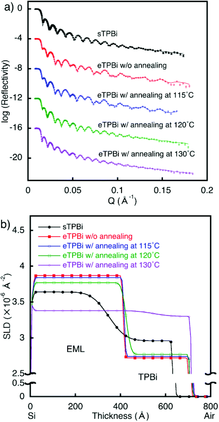 | ||
| Fig. 1 Neutron reflectometry results for sEML/TPBi. (a) Reflectivity profiles and (b) SLD profiles: sEML/sTPBi (closed circles), sEML/eTPBi without annealing (closed squares), and sEML/eTPBi after annealing at 115 °C (open circles), 120 °C (open squares), and 130 °C (open diamonds). The reflectivity scale corresponds to the profile for sEML/sTPBi. For clarity, the other plots in (a) were successively offset by 4 log units. | ||
In the solution process, thermal annealing is required for solvent drying; the effects of thermal annealing on interfaces are important. Extensive interdiffusion was observed in [sEML/sTPBi]; as previously noted, this interdiffusion makes evaluation of only the thermal-annealing effects on the interface structure difficult. Therefore, [sEML/eTPBi] with a sharp interface was used to investigate the annealing effects. The stacked films of [sEML/eTPBi] were annealed at 115 °C, 120 °C, or 130 °C for 10 min. Each NR profile was well fitted using two-organic-layer models (Fig. 1). The reflectivity profile of [sEML/eTPBi] after annealing at 115 °C was approximately the same as that of [sEML/eTPBi] without annealing. This result indicates that annealing at 115 °C did not cause any thermal diffusion and that the interdiffusion in [sEML/sTPBi] occurred during the TPBi coating process before the annealing step. In the film annealed at 120 °C, the SLD of sEML decreased, whereas that of TPBi did not change. This result suggests that only TPBi diffused into sEML, probably because the Tg of BCzBP-d14 is less than the annealing temperature of 120 °C, whereas the Tg of TPBi is greater than the annealing temperature (Table S1†). Thus, sEML was in a (liquid-like) mobile state at the annealing temperature, whereas TPBi remained immobile in a glass state. Consequently, at the [sEML/TPBi] interface, liquid-like sEML eroded the immobile-glass-state TPBi layer and took up TPBi molecules into the sEML, where the TPBi molecules diffused throughout the liquid-like sEML. The sEML molecules could not diffuse into the TPBi layer because the TPBi layer was rigid and lacked sufficient vacancies at the annealing temperature (120 °C). An SLD gradient in sEML was not observed, probably because the diffusion time of TPBi in sEML was too short because of the small thickness of sEML (ca. 40 nm). In the film annealed at 130 °C, which is higher than both Tgs, almost full mixing of the stacked layer was observed. A volume ratio of TPBi in the almost-mixed film was estimated to be approximately 53%. This value is consistent with the ratio between eTPBi thickness and total thickness of the stacked film, [sEML/eTPBi] (58%).
The diffusion of sEML molecules into the TPBi layer in stacked films was also verified by FRET measurements. Fig. 2 shows photoluminescence spectra and plots of photoluminescence intensities at 380 nm emission derived from TPBi and at 515 nm emission derived from Ir(mppy)3. In the [sEML/eTPBi] film, emissions derived from TPBi and Ir(mppy)3 were observed. By contrast, in the [sEML/sTPBi] film, the emission of TPBi was not observed, indicating that sEML molecules diffused into the sTPBi layer during the TPBi coating process and that fluorescence quenching was caused by energy transfer from TPBi to Ir(mppy)3.20,21 This deduction is supported by sufficient spectral overlap between absorption of the Ir(mppy)3 film and photoluminescence of the TPBi film (Fig. S4†).
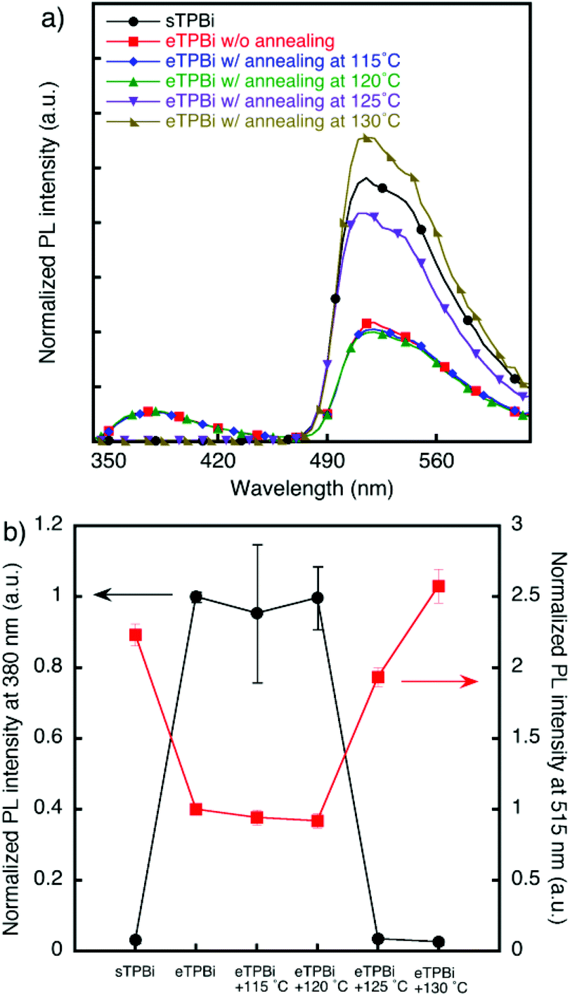 | ||
| Fig. 2 Results from FRET experiments. (a) Photoluminescence spectra of sEML/sTPBi (circles), sEML/eTPBi without annealing (squares), and sEML/eTPBi after annealing at 115 °C (diamonds), 120 °C (triangles), 125 °C (inverted triangles), and 130 °C (rectangular triangles). (b) Normalized photoluminescence intensities of the films at 380 nm emission derived from TPBi and at 515 nm emission derived from Ir(mppy)3. Each error bar represents the maximum and minimum values of three measurement results. | ||
We investigated thermal diffusion in the stacked films. Stacked [sEML/eTPBi] films were annealed at 115 °C, 120 °C, 125 °C, or 130 °C for 10 min. The emission intensity of TPBi drastically decreased in the case of the film annealed at 125 °C, which is higher than the Tgs of BCzBP and TPBi; this diminished emission intensity therefore indicates quenching by Ir(mppy)3 that diffused into the eTPBi layer. By contrast, the emission intensity of Ir(mppy)3 increased in the case of films annealed at temperatures greater than 125 °C. This result also indicates energy transfer from TPBi to Ir(mppy)3.
Next, we evaluated trilayer films, which represent more realistic device structures than the bilayer films. The fabricated trilayer films were [PTPD/eEML/eTPBi], [PTPD/sEML/eTPBi], and [PTPD/sEML/sTPBi] prepared on Si wafers. sEML and sTPBi were annealed at 115 °C. Fig. 3 shows the NR profiles of the trilayer films. The profiles were very well fitted to three-organic-layer models, indicating successful characterization of the trilayer film. The obtained interface structures were the same as those obtained in the bilayer experiments.16 We also quantitatively calculated materials distribution along the depth direction using SLD values of the corresponding single-layer films (Fig. S5†). Notably, the two types of solution-processed interfaces, [PTPD/sEML] and [sEML/sTPBi], exhibited different shapes. In the [PTPD/sEML] interface, sEML molecules largely diffused into the PTPD layer and increased the SLD of the PTPD layer; however, PTPD only slightly diffused into the sEML. By contrast, in the [sEML/sTPBi] interface, both sEML molecules and TPBi largely diffused into the other layer. We assume that the different interface shapes resulted from the difference in molecular diffusivity between layer molecules during the solution-processed stacking. Small molecules exhibit a higher diffusivity than polymers, resulting in the interdiffused [sEML/sTPBi] interface. Fig. 4 shows the energy diagram of the three types of trilayer films.
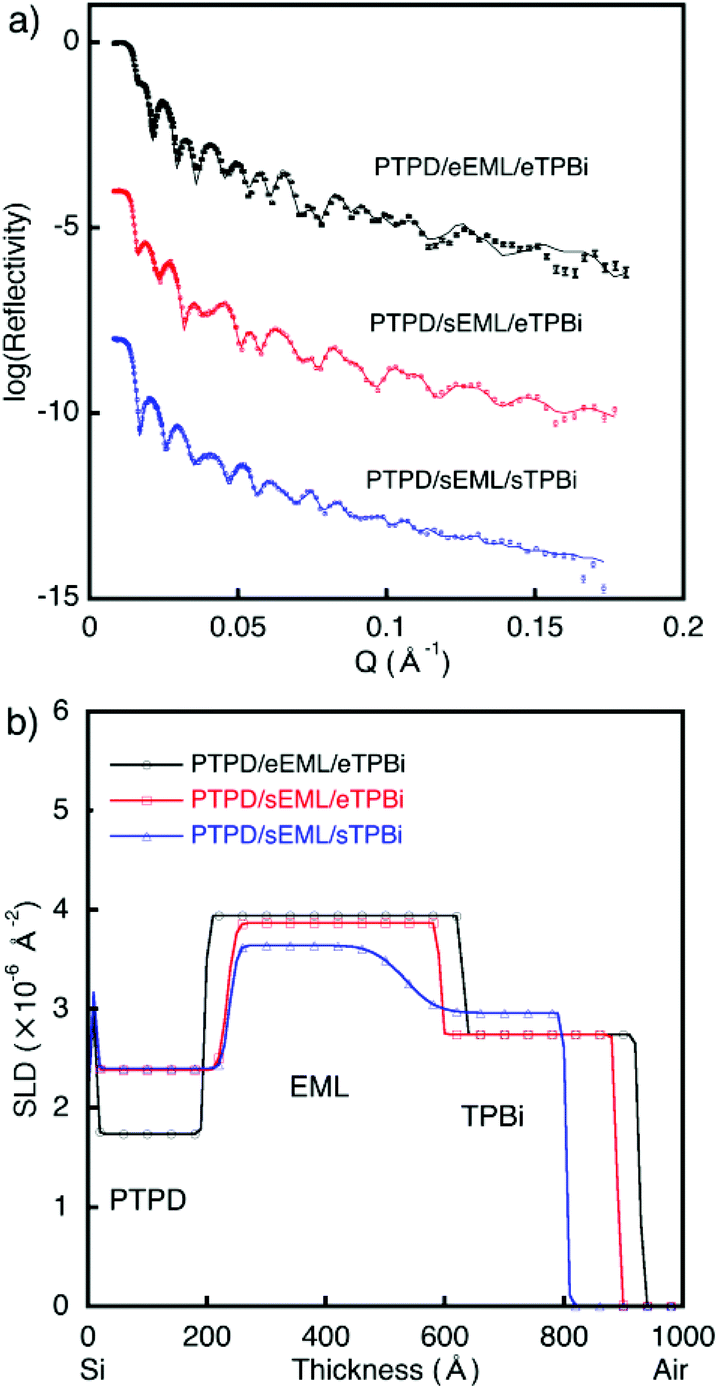 | ||
| Fig. 3 Neutron reflectometry results of trilayer stacked films. (a) Reflectivity profiles and (b) scattering density profiles (SLDs) of Si/PTPD/eEML/eTPBi (circles), Si/PTPD/sEML/eTPBi (squares), and Si/PTPD/sEML/sTPBi (triangles). The reflectivity scale corresponds to the profile of Si/PTPD/eEML/eTPBi. For clarity, the other plots in (a) were successively offset by 4 log units. | ||
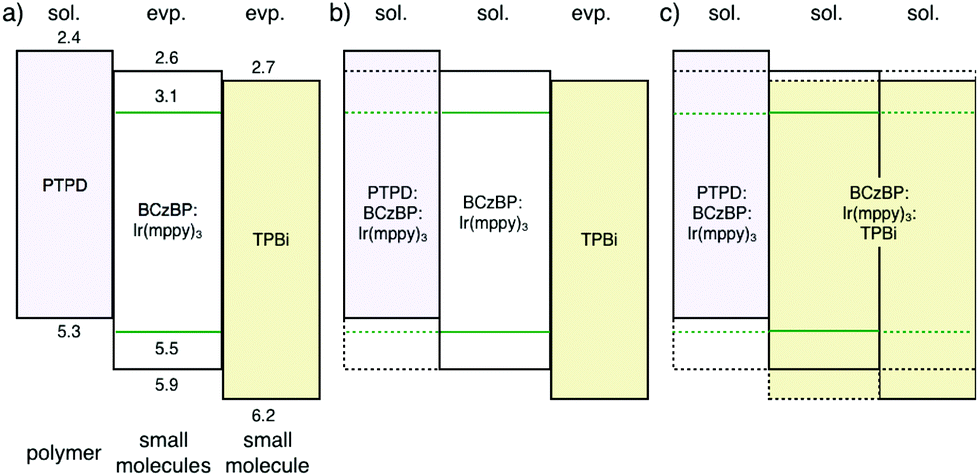 | ||
| Fig. 4 Energy diagram of trilayer stacked films: (a) PTPD/eEML/eTPBi, (b) PTPD/sEML/eTPBi, and (c) PTPD/sEML/sTPBi. | ||
We fabricated OLEDs with structures of [ITO (130 nm)/poly(3,4-ethylenedioxythiophene):poly(4-styrenesulfonate) (PEDOT:PSS) (40 nm)/PTPD (20 nm)/BCzBP:9 wt% Ir(mppy)3 (40 nm) as eEML or sEML/TPBi (30 nm) as sTPBi or eTPBi/8-quinolinolato lithium (Liq) (1.5 nm)/Al (100 nm)], in which eEML and eTPBi were either non-annealed or annealed. The fabricated device structures are given below:
Device A1: ITO/PEDOT:PSS/PTPD/sEML/sTPBi/Liq/Al
Device A2: ITO/PEDOT:PSS/PTPD/eEML (annealed)/eTPBi (annealed)/Liq/Al
Device B1: ITO/PEDOT:PSS/PTPD/eEML/eTPBi/Liq/Al
Device B2: ITO/PEDOT:PSS/PTPD/sEML/eTPBi/Liq/Al
Device B3: ITO/PEDOT:PSS/PTPD/eEML (annealed)/eTPBi/Liq/Al
Here, Devices B1–B3 with non-annealed eTPBi are the same devices reported in our previous paper, where details of the devices are discussed (Fig. 5).16 Current density–voltage–luminance and current efficiency–current density characteristics of the devices are shown in Fig. 5 and S6.† Devices B1–B3 exhibited nearly the same driving voltages, irrespective of the different [PTPD/EML] interface structures that strongly influence the hole-injection characteristics. This consistency of the driving voltage suggests that the dominant charge carrier in the devices’ EML was electrons and that the charge recombination zone was near the [PTPD/EML] interface. By contrast, Devices A1–A2 showed much higher driving voltages than Devices B1–B3. In Devices B1–B3, the small molecules of EML and TPBi could not diffuse into the layer of the other material because the eTPBi layers were not annealed. However, in Devices A1–A2, small molecules of EML and TPBi did diffuse into the layer of the other material because the TPBi layer was spin coated or the eTPBi layer was annealed. The electron affinity (EA) of BCzBP is smaller than that of TPBi; however, the EA of Ir(mppy)3 is larger than that of TPBi. Therefore, electrons were trapped by Ir(mppy)3 in the TPBi layer, resulting in large increases in driving voltage. Devices B2–B3 exhibited higher current efficiencies than Device B1. This improvement is ascribed to suppressed triplet-polaron quenching at the ambiguous [PTPD/EML] interface in Devices B2–B3; this suppressed quenching is due to fewer accumulated holes than at the sharp [PTPD/eEML] interface in Device B1. Devices A1 and B2, which both include an sEML, exhibited nearly the same current efficiency–current density characteristics, although Device A1 exhibited much higher driving voltages than Device B2. Likewise, Devices A2 and B3, which both include an annealed eEML, exhibited nearly the same current efficiency–current density characteristics, although Device A2 showed much higher driving voltages than Device B3. These consistencies can also be explained by the assumption that the dominant charge carrier in the EML was electrons. In the devices, holes flow poorly in the EML because of the low hole mobility stemming from the hole hopping conduction mechanism at doped Ir(mppy)3 sites. Most injected holes should be near the PTPD in the EML, resulting in a high hole concentration in the EML region. The injected electrons that flow through the EML recombine with the holes at the EML region with very high probability, generating light emission. Thus, luminance was determined by the amount of flowing electron current, resulting in a consistent current efficiency (cd A−1).
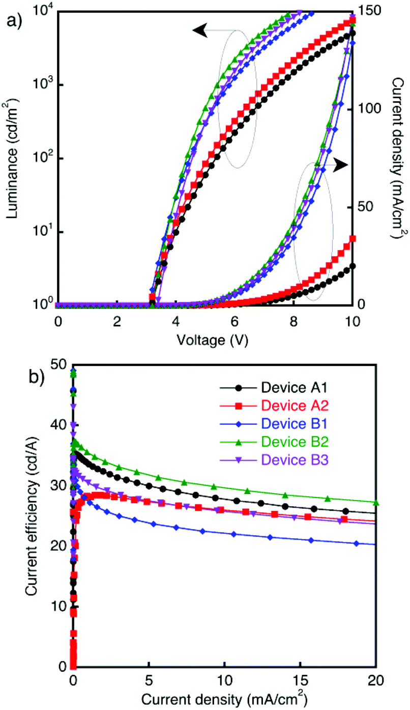 | ||
| Fig. 5 OLED characteristics. (a) Current density–voltage–luminance (JVL) characteristics and (b) current density–current efficiency characteristics of OLEDs with sEML/sTPBi (Device A1: black closed circles), eEML (annealed)/eTPBi (annealed) (Device A2: red closed squares), eEML/eTPBi (Device B1: blue closed diamonds), sEML/eTPBi (Device B2: green triangles), and eEML (annealed)/eTPBi (Device B3: purple inverted triangles). | ||
Conclusions
We succeeded in comprehensively evaluating the solution-processed small-molecule interfaces in OLEDs and discussed the influence of the interface structures on the device characteristics. We investigated the interfaces between a BCzBP-d14:Ir(mppy)3 EML and a TPBi ETL using NR and FRET analyses. These molecules largely interdiffused during the TPBi layer coating process. We also investigated the effects of thermal annealing on the interface structures and observed asymmetric diffusion of TPBi into the BCzBP-d14:Ir(mppy)3 layer as a result of the diffusivity difference among the molecules at the annealing temperatures. We successfully evaluated [PTPD/BCzBP-d14:Ir(mppy)3/TPBi] trilayer films and observed different shaped interfaces between [PTPD/sEML] and [sEML/sTPBi] interfaces. In the OLEDs, we observed that the mixed interface resulting from solution processing did not only adversely affect the device characteristics, such as by increasing the driving voltage, but also the mixed interface beneficially affected device performance by, for example, suppressing charge accumulation at the interface. To develop highly efficient solution-processed OLEDs, precise control of the interface structure is important. The findings obtained in this work are useful in developing not only solution-processed OLEDs but also other solution-processed devices. We hope our findings in this work advance the development of such devices.We would like to thank Sho Kagami for DSC measurements. We would like to thank the “Strategic Promotion of Innovative R&D Program” of Japan Science and Technology Agency (JST) for financial support. The NR experiments were performed with the SOFIA reflectometer22,23 and approved by the Neutron Science Proposal Review Committee of J-PARC MLF (Proposal No. 2014A0304) and supported by the Inter-University Research Program on Neutron Scattering of IMSS, KEK. Y.-J. Pu thanks the PRESTO (Sakigake), JST for support.
References
- N. Aizawa, Y.-J. Pu, M. Watanabe, T. Chiba, K. Ideta, N. Toyota, M. Igarashi, Y. Suzuri, H. Sasabe and J. Kido, Nat. Commun., 2014, 5, 5756 CrossRef PubMed.
- A. C. Arias, J. D. MacKenzle, I. McCulloch, J. Rivnay and A. Salleo, Chem. Rev., 2010, 110, 3–24 CrossRef CAS PubMed.
- L. Duan, L. Hou, T.-W. Lee, J. Qiao, D. Zhang, G. Dong, L. Wang and Y. Qiu, J. Mater. Chem., 2010, 20, 6392–6407 RSC.
- T. Earmme, E. Ahmed and S. A. Jenekhe, Adv. Mater., 2010, 22, 4744–4748 CrossRef CAS PubMed.
- K. S. Yook and J. Y. Lee, Adv. Mater., 2014, 26, 4218–4233 CrossRef CAS PubMed.
- C. Zhong, C. Duan, F. Huang, H. Wu and Y. Cao, Chem. Mater., 2011, 23, 326–340 CrossRef CAS.
- N. Ide, K. Yamae, V. Kittichungchit, H. Tsuji, M. Ota and T. Komoda, J. Photopolym. Sci. Technol., 2014, 27, 357–361 CrossRef.
- K. Kato, T. Iwasaki and T. Tsujimura, J. Photopolym. Sci. Technol., 2015, 28, 335–340 CrossRef CAS.
- H. Sasabe and J. Kido, Eur. J. Org. Chem., 2013, 7653–7663 CrossRef CAS.
- H. Sasabe and J. Kido, J. Mater. Chem. C, 2013, 1, 1699 RSC.
- A. J. Clulow, C. Tao, K. H. Lee, M. Velusamy, J. A. McEwan, P. E. Shaw, N. L. Yamada, M. James, P. L. Burn, I. R. Gentle and P. Meredith, Langmuir, 2014, 30, 11474–11484 CrossRef CAS PubMed.
- A. M. Higgins, A. Cadby, D. G. Lidzey, R. M. Dalgliesh, M. Geoghegan, R. A. L. Jones, S. J. Martin and S. Y. Heriot, Adv. Funct. Mater., 2009, 19, 157–163 CrossRef CAS.
- A. M. Higgins, S. J. Martin, M. Geoghegan, S. Y. Heriot, R. L. Thompson, R. Cubitt, R. M. Dalgliesh, I. Grizzi and R. A. L. Jones, Macromolecules, 2006, 39, 6699–6707 CrossRef CAS.
- D. Mon, A. M. Higgins, D. James, M. Hampton, J. E. Macdonald, M. B. Ward, P. Gutfreund, S. Lilliu and J. Rawle, Phys. Chem. Chem. Phys., 2015, 17, 2216–2227 RSC.
- S. Ohisa, G. Matsuba, N. L. Yamada, Y.-J. Pu, H. Sasabe and J. Kido, Adv. Mater. Interfaces, 2014, 1, 1400097 CrossRef.
- S. Ohisa, Y.-J. Pu, N. L. Yamada, G. Matsuba and J. Kido, ACS Appl. Mater. Interfaces, 2015, 7, 20779–20785 CAS.
- A. R. G. Smith, K. H. Lee, A. Nelson, M. James, P. L. Burn and I. R. Gentle, Adv. Mater., 2012, 24, 822–826 CrossRef CAS PubMed.
- C. Tao, M. Aljada, P. E. Shaw, K. H. Lee, H. Cavaye, M. N. Balfour, R. J. Borthwick, M. James, P. L. Burn, I. R. Gentle and P. Meredith, Adv. Energy Mater., 2013, 3, 105–112 CrossRef CAS.
- J. A. McEwan, A. J. Clulow, P. E. Shaw, A. Nelson, T. A. Darwish, P. L. Burn and I. R. Gentle, Adv. Mater. Interfaces, 2016, 3, 1600184 CrossRef.
- D. L. Dexter, J. Chem. Phys., 1953, 21, 836–850 CrossRef CAS.
- T. Förster, Discuss. Faraday Soc., 1959, 27, 7–17 RSC.
- N. L. Yamada, N. Torikai, K. Mitamura, H. Sagehashi, S. Sato, H. Seto, T. Sugita, S. Goko, M. Furusaka, T. Oda, M. Hino, T. Fujiwara, H. Takahashi and A. Takahara, Euro. Phys. J. Plus, 2011, 126, 108 CrossRef.
- K. Mitamura, N. L. Yamada, H. Sagehashi, N. Torikai, H. Arita, M. Terada, M. Kobayashi, S. Sato, H. Seto, S. Gokou, M. Furusaka, T. Oda, M. Hino, H. Jinnai and A. Takahara, Polym. J., 2013, 45, 100–108 CrossRef CAS.
Footnote |
| † Electronic supplementary information (ESI) available. See DOI: 10.1039/c6nr06654b |
| This journal is © The Royal Society of Chemistry 2017 |