
Laser-patterned functionalized CVD-graphene as highly transparent conductive electrodes for polymer solar cells
Luca
La Notte
a,
Enrica
Villari
a,
Alessandro Lorenzo
Palma
 a,
Alberto
Sacchetti
b,
Maria
Michela Giangregorio
b,
Giovanni
Bruno
b,
Aldo
Di Carlo
a,
Giuseppe Valerio
Bianco
*b and
Andrea
Reale
*a
a,
Alberto
Sacchetti
b,
Maria
Michela Giangregorio
b,
Giovanni
Bruno
b,
Aldo
Di Carlo
a,
Giuseppe Valerio
Bianco
*b and
Andrea
Reale
*a
aCHOSE (Centre for Hybrid and Organic Solar Energy), Department of Electronic Engineering, University of Rome Tor Vergata, via del Politecnico 1, 00133 Rome, Italy. E-mail: reale@ing.uniroma2.it
bCNR-NANOTEC Institute of Nanotechnology, Apulian Graphene Lab, Department of Chemistry, University of Bari, via Orabona 4, Bari, 70126, Italy. E-mail: giuseppevalerio.bianco@cnr.it
First published on 22nd November 2016
Abstract
A five-layer (5L) graphene on a glass substrate has been demonstrated as a transparent conductive electrode to replace indium tin oxide (ITO) in organic photovoltaic devices. The required low sheet resistance, while maintaining high transparency, and the need of a wettable surface are the main issues. To overcome these, two strategies have been applied: (i) the p-doping of the multilayer graphene, thus reaching 25 Ω □−1 or (ii) the O2-plasma oxidation of the last layer of the 5L graphene that results in a contact angle of 58° and a sheet resistance of 134 Ω □−1. A Nd:YVO4 laser patterning has been implemented to realize the desired layout of graphene through an easy and scalable way. Inverted Polymer Solar Cells (PSCs) have been fabricated onto the patterned and modified graphene. The use of PEDOT:PSS has facilitated the deposition of the electron transport layer and a non-chlorinated solvent (ortho-xylene) has been used in the processing of the active layer. It has been found that the two distinct functionalization strategies of graphene have beneficial effects on the overall performance of the devices, leading to an efficiency of 4.2%. Notably, this performance has been achieved with an active area of 10 mm2, the largest area reported in the literature for graphene-based inverted PSCs.
Introduction
Organic photovoltaics (OPV) has emerged as a technology for the fabrication of low cost, thinner and more flexible devices compared with the conventional photovoltaics, thus making them suitable for a host of applications beyond rooftop and solar-farm panels.1,2 A marked improvement in Power Conversion Efficiency (PCE), exceeding 10%, has been achieved owing to the introduction of low band gap donors that tune the absorption spectrum, energy levels, crystallinity, and charge carrier mobility to enhance performance.3–5 Such polymer donors have also presented encouraging results even when processed with non-chlorinated solvents.6–8 State-of-the art Polymer Solar Cells (PSCs) use indium tin oxide (ITO) as a transparent conductive electrode, but ITO presents some drawbacks: the release of oxygen and indium into the organic layer, the poor transparency in the blue region and the stiffness that discourages its use in flexible devices. Recently, it has been demonstrated that graphene is a promising candidate to replace ITO as the electrode in OPV due to its unique physical, electrical, mechanical and optical properties. In particular, graphene has an intrinsic work function of 4.5 eV that can be tuned from 3.25 eV to 5.10 eV,9 covering a wide range of anode and cathode applications and allowing a good energy band alignment with charge transport layers. Moreover, it is possible to achieve comparable or even higher transmittance than provided by ITO with four or less layers of graphene.10 Actually, graphene has some challenges to face such as the high sheet resistance (often larger than 1 kΩ □−1 for a single layer) and high cost of fabrication that limit the development of graphene-based electrodes as an alternative to ITO technology. Several solutions have been suggested to significantly reduce the sheet resistance of graphene, including multilayer structures and material doping. Although several citations confirm the achievement of a 4-layer graphene film with 30 Ω □−1 (through a doping process based on HNO3 treatment),11 the described procedure does not produce, easily, when used by others,12,13 a low-sheet resistance performance. Recently, the lowest sheet resistance of graphene films achieved through a SOCl2 doping has been around 27 Ω □−1 with a transmittance of 87%.14 Among the typical methods for the preparation and production of graphene, Chemical Vapor Deposition (CVD) is a technique that ensures good quality films by means of a reproducible and industrially scalable method.15–17 After synthesis, the as-grown graphene can be transferred to insulator substrates such as glass and PET. Moreover, graphene is inherently inert, therefore it is highly resistant in acidic environments.17 Most groups have employed CVD graphene as electrodes in OPV. De Arco et al. have reported PSCs on PET/graphene substrates showing comparable performance with devices on standard PET/ITO, and capability to operate under strong bending conditions.18 Other studies have obtained PCEs in the range of 2.5–3% by fabricating devices on glass/graphene.19,20 A significant leap forward has been achieved by Park et al. who have presented direct and inverted flexible PSCs with a record-high PCE of 6.1 and 7.1%, respectively.21 Interestingly, graphene has been also applied as the top electrode by using a lamination process.22 However, the mentioned studies do not report the active area of the devices or they refer to very small areas, from 0.75 mm2 to 4.6 mm2, indicating the difficulty in obtaining uniform graphene on a larger area. The largest area (10 mm2) has been presented by Jin An et al.23 but the structure of the device is based on a direct configuration known to be not industrially relevant and less appropriate for polymer:fullerene systems than the inverted design.24,25This work tackles the issues that still hinder the use of CVD graphene in OPV by functionalizing the layer to improve its poor wettability and to significantly decrease the sheet resistance (RS). Two distinct strategies have been applied: (i) the p-doping of the multilayer graphene thus reaching 25 Ω □−1 or (ii) the oxygen-plasma oxidation of the last layer of the 5L graphene that results in a contact angle of 58° and a sheet resistance of 134 Ω □−1. We report the fabrication of inverted PSCs on the functionalized graphene with an area of 10 mm2. In particular, graphene functionalized by oxygen (O2) plasma treatment has demonstrated to act as an effective electrode leading to a maximum PCE of 4.2%. Notably, this performance has been achieved by using an active layer processed with non-chlorinated solvents. Moreover, a laser patterning has been introduced as a reliable and scalable method to pattern graphene. In fact, laser processing enables non-contact, highly precise, selective, highly automated and economically convenient fabrication processes, also for the emergent photovoltaics.26,27 With respect to other etching techniques, including the traditional photo-lithography, which imply the usage of expensive sacrificial elements, laser processing only involves laser apparatus, allowing zero costs connected to consumables, i.e. etching medium and shadow masks.
Results and discussion
Graphene requires a high transmittance in the visible region, a low sheet resistance and an appropriate work function to act as a cathode in OPV. Moreover, graphene properties should be compatible with the solution processing typically used in the fabrication of PSCs. In fact, a critical issue is the hydrophobicity of the graphene surface that hinders the deposition of uniform layers by solution processing. In this work, graphene has been synthesized and suitably functionalized by O2 plasma treatment in order to improve the wettability or by SOCl2 doping to increase the conductivity. Subsequently, the modified graphene has been applied as the bottom electrode in inverted PSCs.The Raman spectrum of CVD graphene used in this work is reported in Fig. 1 (red line). The peaks of the first order Raman G mode and of the second order 2D one are clearly visible on the fluorescence background due to the supporting Corning glass substrate. No D peak can be discriminated in the graphene spectrum owing to the fluorescence background. However, the Raman spectrum for the same graphene supported on Si/SiO2 shows a D peak (around 1350 cm−1) whose intensity is well below 5% of the G peak, thus attesting for its good structural quality. Significant modification in the Raman response can be observed upon chemical modification of graphene by SOCl2 doping (blue line) or O2 plasma treatment (black line). Specifically, the p-doping effect due to the SOCl2 treatment is reflected by the shift toward higher wavenumbers of the G (from 1582 to 1597 cm−1) and 2D peaks (from 2674 to 2688 cm−1) as expected according to the literature.28 The higher charge carrier density also causes the narrowing of the G peak bandwidth from 11 to 9 cm−1 and the decrease of the ratio between the intensities of 2D and G peaks (from 1.79 to 1.13) due to the suppression of the Kohn anomaly.29 No D peak can be observed even after doping, thus, attesting that the graphene chemical modification by SOCl2 treatment does not introduce new Csp3 sites acting as charge scattering centers.14 Conversely, an intense D peak results upon plasma oxidation since graphene interaction with oxygen atoms involves the breaking of C–C π-bonds, thus, decorating graphene with polar C–O bonds (carboxyl, hydroxyl, and epoxy groups). Such structural modifications also cause the enlargement of the G peak due to its convolution with the emerging D′ peak above 1600 cm−1 and the decrease in intensity of the 2D peak.29–31 Here, it is important to underline that the plasma oxidation, monitored in real time by spectroscopic ellipsometry, has been carried out under mild modulated plasma conditions in order to avoid carbon ablation and amorphization.
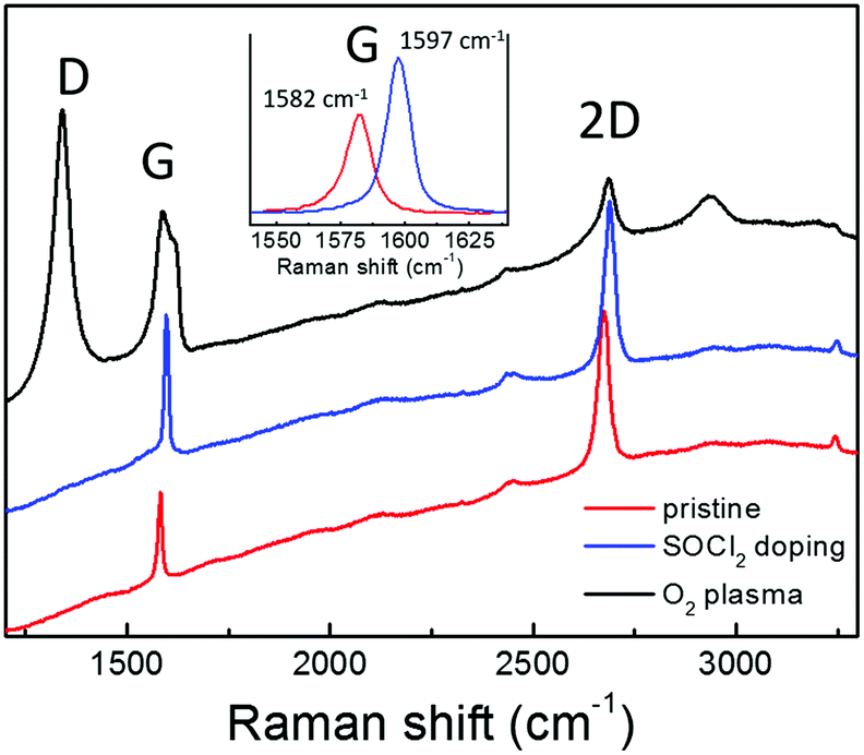 | ||
| Fig. 1 Raman spectra of CVD graphene (single layer) supported on Corning glass before any treatment (pristine) and after SOCl2 doping or O2 plasma treatment (60′′ of treatment time). Details of the G peak shift, narrowing and increase in intensity upon SOCl2 doping are shown in the inset. | ||
Fig. 2 shows the sheet resistance values of pristine, O2 plasma treated and SOCl2 chemical doped CVD graphene/glass samples with 1–5 stacked layers of graphene. The sheet resistance value of the pristine CVD graphene decreases by one order of magnitude going from the monolayer to the five-layers. Graphene foils act as parallel resistors whose specific RS is further lowered by the “patch effect”. Specifically, high-resistivity defects (e.g. cracks, grain boundaries, wrinkles, etc.) in one film are bridged by neighbouring layers, thus, decreasing the average RS of each layer (estimated ≈500 Ohm sq−1).32
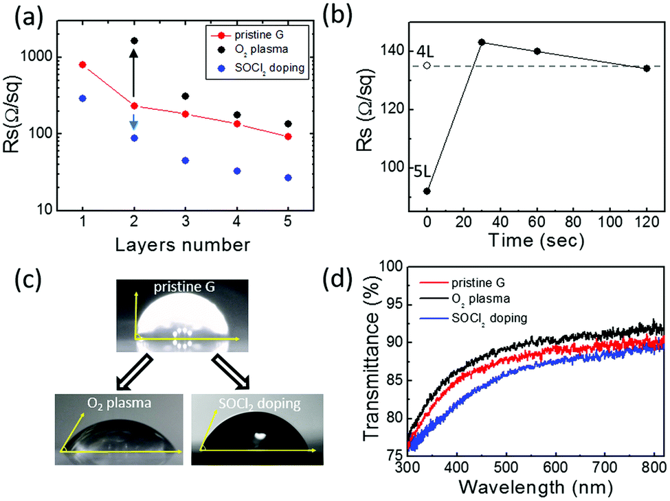 | ||
| Fig. 2 (a) RS value of 1-to-5-layer graphene samples as transferred on glass (pristine G), after 120 s of O2/He modulated plasma treatment (O2 plasma), and after thermal treatment with SOCl2 (SOCl2 doping). (b) Evolution of the RS value of 5L graphene upon 120 s of O2/He modulated plasma treatment (the RS value of pristine 4L graphene is also reported). (c) Water contact angle of 5L graphene before and after 120 s of plasma treatment and SOCl2 doping. (d) Transmittance spectra of pristine, O2 plasma treated and SOCl2 doped 5L graphene samples. | ||
The chemical doping by SOCl2 thermal treatment provides an almost three-fold decrease in the RS of both mono and multilayer graphene samples. This is expected to derive from an increased hole concentration due to the covalent attachment of electron acceptor chlorine atoms at graphene defect sites with hydroxyl and carboxyl functionalities.33,34
The plasma-functionalization of graphene with oxygen species provides significant effects on its conduction properties. In contrast to the SOCl2 chemical doping, the influence of the functionalization processes on the RS of graphene samples depends on the number of graphene foils: the higher the number of stacked graphene foils, the lower the relative variation of RS. Specifically, after plasma oxidation the resistivity of single layer graphene became so high that the measurement of its RS was not possible with our Van der Pauw experimental setup. For increasing graphene layer numbers, an RS increase of one order of magnitude for the bilayer sample and an RS increase below 50% for the five-layers are observed. This indicates that the functionalization process is mainly confined to the outer graphene layer as already reported by Gokus et al.35 This is also evident in the graphene RS evolution upon O2 plasma treatment reported in Fig. 2(b). The figure shows that the plasma oxidation of the 5L graphene initially causes an increase in its RS that, for longer plasma-treatment times, stabilizes to an RS value comparable to the 4L graphene one. Similarly, data reported in Fig. 2(a) shows that the RS value of the functionalized 4L graphene is fully comparable with the RS of the pristine 3L graphene. Thus, when the treatment time is long enough (i.e. 120 s), important structural modifications limit the conduction in the top graphene layer (see Fig. 1). As a consequence, the RS values of the oxidized 5- and 4-layer samples result similar to the RS values of, respectively, the pristine 4-layer and 3-layer ones.
Fig. 2(c) and (d) show the effects of the two functionalization strategies on the wettability and transparency of a five-layer graphene sample. As expected, the O2 plasma treatment strongly enhances the graphene wettability providing a decrease of the water contact angle from 90° (pristine graphene) to 58° (O2 plasma). Interestingly, SOCl2 chemical doping also influences the five-layer graphene wettability that shows a water contact angle of 68° (SOCl2 doping). This can be related to the covalent attachment of electronegative chlorine atoms which makes the graphene surface more polar as well as to the doping-dependent wettability effects on graphene.36 Finally, Fig. 2(d) shows that oxygen plasma treatment results in a lower absorption of the multilayer graphene probably due to carbon ablation from the graphene top layer. Conversely, the higher optical absorption after SOCl2 treatment may be attributed to the presence of Cl and S species on graphene.
Graphene substrates need to be patterned to allow the realization of devices with the desired layout (5 × 2 mm2). CVD graphene has the advantage to be processed with a top-down approach by using already existing patterning methods.37 A Nd:YVO4 laser, whose emission wavelength (λ = 1064 nm) was converted to λ = 532 nm through a nonlinear crystal, was investigated to selectively etch graphene previously deposited by CVD in the form of square films covering almost an entire glass of 25 × 25 mm2. It was found that a laser fluence of 40 mJ cm−2 is sufficient to remove graphene without engraving the glass. Fig. 3(a) displays the pattern performed by a single laser run on a sample placed on a stage moving at 20 cm s−1. The pattern is a well-defined line with a width of 160 μm. Multiple runs define the space between two graphene stripes used in the layout for the fabrication of the devices (Fig. 3(b)).
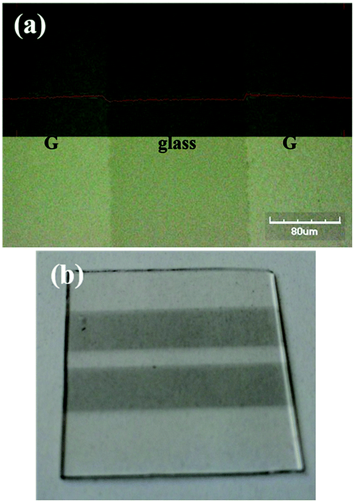 | ||
| Fig. 3 (a) Optical microscope image of the removed graphene with a single laser run (upper side: profile line of the surface). (b) Photo of the patterned graphene/glass substrate. | ||
Graphene shows sensitivity towards typical electron transport layers in OPV because of the introduction of defects in graphene.22 It has been demonstrated that the deposition of PEDOT:PSS has a beneficial effect of protecting graphene, thus allowing the deposition of a good quality zinc or titanium oxide. This leads to improved reproducibility and device yield as well.38 For these reasons, PEDOT:PSS, modified with 2-propanol at a 3![[thin space (1/6-em)]](https://www.rsc.org/images/entities/char_2009.gif) :1 ratio (v/v) to improve the wetting on graphene39 has been applied onto graphene. The insertion of PEDOT:PSS leads to the inverted structure depicted in Fig. 4.
:1 ratio (v/v) to improve the wetting on graphene39 has been applied onto graphene. The insertion of PEDOT:PSS leads to the inverted structure depicted in Fig. 4.
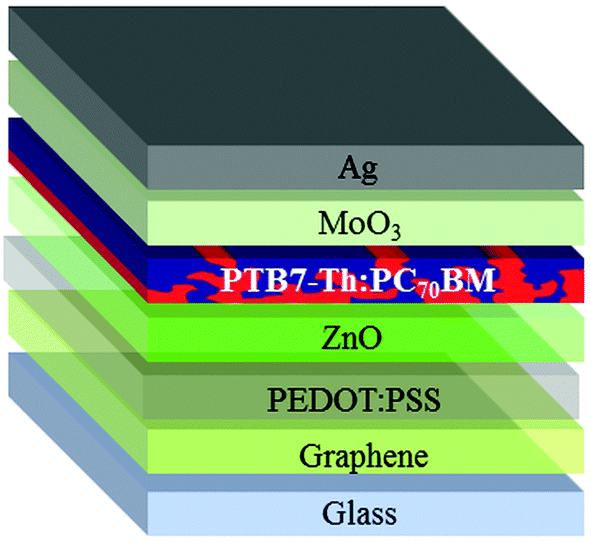 | ||
| Fig. 4 Structure of the inverted device on the graphene/glass substrate. | ||
In order to maximize device performances over a relatively large area of 10 mm2, we pursued the high conductivity of graphene electrodes, therefore only 5L graphene has been used as the electrode.
The modified PEDOT:PSS was firstly inserted in ITO-based devices to evaluate the influence of such typical hole transport layer between the cathode and zinc oxide used as an electron transport layer. As reported in Fig. 5, PEDOT:PSS thickness affects FF and JSC whereas VOC remains stable.
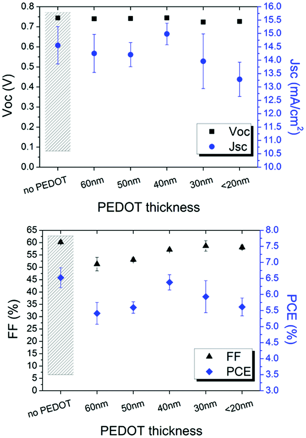 | ||
| Fig. 5 Electrical parameters of the ITO-based inverted devices as a function of the PEDOT thickness. A device without PEDOT is shown as reference. | ||
It is found that 40 nm is the suitable thickness; thicker layers cause higher light absorption and, thus, lower current. Interestingly, the efficiency of the device comprising ITO/PEDOT/ZnO layers is comparable to the device based on the typical ITO/ZnO cathode configuration. This behaviour is attributed to the electron transport property shown when IPA is added to PEDOT:PSS.40
The stack ZnO/PTB7-Th:PC70BM/MoO3/Ag has been transferred onto the graphene substrates with the optimized PEDOT:PSS. As reported in Table 1, the functionalized graphene allows one to achieve higher performing devices than the pristine graphene. In the latter case, the device shows a resistor-like behaviour with poor photo-response. This is explainable with a not suitable PEDOT:PSS coating due to the high contact angle of the graphene surface. Furthermore, the use of only solvent modification of PEDOT:PSS as a strategy to improve the wettability of graphene is not sufficient because it gives rise to 50% device yield.39
| Cathode | V OC (V) | J SC (mA cm−2) | FF (%) | PCE (%) |
|---|---|---|---|---|
| ITO | 0.76 ± 0.004 | 15.05 ± 0.19 | 57.3 ± 0.55 | 6.52 ± 0.1 |
| Pristine graphene | 0.37 ± 0.11 | 6.36 ± 1.37 | 25.9 ± 0.93 | 0.63 ± 0.34 |
| O2 plasma-treated graphene | 0.75 ± 0.005 | 13.08 ± 0.16 | 41.5 ± 1.74 | 4.07 ± 0.19 |
| SOCl2 doped graphene | 0.72 ± 0.02 | 12.68 ± 0.34 | 39.2 ± 3.5 | 3.61 ± 0.47 |
Between the two modified graphene films, the devices based on the plasma-treated graphene exhibit better electrical parameters than PSCs built on the chemically-doped graphene. It seems that the doped graphene establishes a good Ohmic contact for the collection of electrons but the control of the interface processability of graphene is more critical than the film conductivity. Therefore, the improved wettability guaranteed by O2 plasma treatment is sufficient to allow the fabrication of efficient devices. Anyway, the benefit of doping (lower sheet resistance) is expected to play a major role when devices are built on electrodes with larger areas.41,42
The relatively lower PCE of the graphene electrode compared to the conventional ITO electrode is mainly determined by FF. In fact, ITO has comparable wettability43 (56°) but lower sheet resistance (10 Ω sq−1) with respect to the plasma treated graphene, and it is more wettable as compared to the doped graphene. Furthermore, ITO shows a better transparency than graphene around 400 nm (the related transmittance is incorporated in Fig. 7). It is worth noting that significant results of the graphene electrodes have been obtained for an active area of 10 mm2, demonstrating the quality and uniformity of the synthesized and treated CVD graphene over a large area.
Fig. 6 shows the J–V curve of the best performing device based on the O2 plasma-treated graphene as the bottom electrode. To our knowledge this polymer solar cell presents the best efficiency conversion (4.2%) among the devices with an area ≥10 mm2 in the literature.
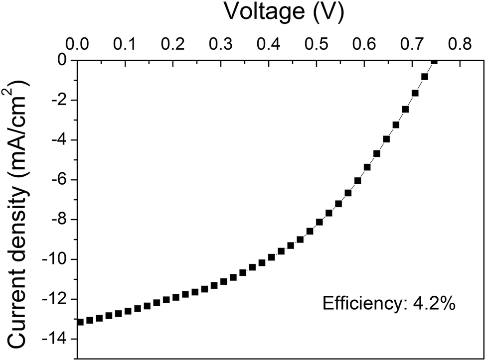 | ||
| Fig. 6 J–V curve of the device based on the O2 plasma-treated graphene showing the maximum efficiency. | ||
The external quantum efficiency (EQE) spectra of the devices showing the best performances on ITO, plasma treated and chemically doped graphene have been acquired and shown in Fig. 7. Polymer solar cells based on PTB7-Th cover the whole visible region until 800 nm. At lower wavelengths, the spectrum profile of the graphene-based devices differs from the profile of the ITO-based ones, probably due to a different growth of the stack on the graphene substrate. In particular, the peaks at 370 and 470 nm are more pronounced in ITO-based devices, thus allowing a higher JSC than graphene anodes.
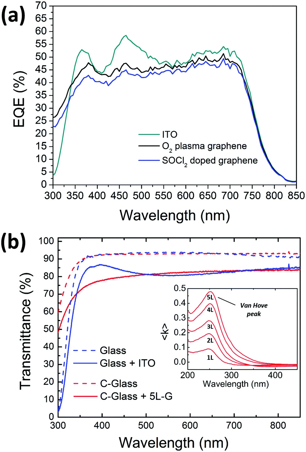 | ||
| Fig. 7 (a) External quantum efficiency of the inverted devices based on three different anodes. (b) Transmittance spectra of electrodes based on ITO and 5L graphene and of their supporting glass (glass) and Corning glass (c-glass) substrates, respectively. Details of the van Hove peaks in the pseudoextinction coefficient spectra (acquired by spectroscopic ellipsometry) of mono and multilayer graphene are reported in the inset. | ||
The EQE of the device based on the plasma-treated graphene is slightly higher than the cell comprising the doped one; this is explainable with the higher transmittance of the plasma-treated graphene as seen in Fig. 2(d). This is consistent with the data measured under a sun simulator as shown in Table 1.
In the nearest UV region (below 350 nm), the large difference in EQE between ITO- and graphene-based cells is related to the different type of glass, being Corning-glass used for graphene more transparent than the one used for the commercial ITO/glass electrode (see Fig. 7(b)). However, a more detailed analysis of the EQE in the UV region should consider the efficient absorption of the multilayer graphene due to the exciton-shifted van Hove singularity in its density of states (see the inset in Fig. 7(b)).
Conclusions
In the attempt to replace ITO as a transparent electrode in polymer solar cells, CVD graphene would represent a good candidate if it accommodates the typical requirements of solution processing and presents high transmittance and low sheet resistance. In this work, graphene deposited by CVD has been functionalized by two distinct strategies: by exposing the surface to oxygen plasma to improve wettability (water contact angle from 90° to 58°) or by doping the film to decrease sheet resistance down to 25 Ω □−1 with 87% of transmittance at 550 nm. Such modified graphene films have been suitably patterned by an easy and reproducible way based on Nd:YVO4 laser technology. Inverted polymer solar cells have been fabricated by firstly applying PEDOT:PSS to the patterned graphene to protect it from the overlying zinc oxide. Successively, the active layer, processed with non-chlorinated solvents, MoO3 and Ag complete the structure. The devices based on graphene functionalized by plasma treatment or doped by SOCl2 exhibit an average efficiency of about 4% whereas the 5L pristine graphene electrode gives an efficiency well below 1%. This demonstrates that the effect of the improvement of the surface wettability is important, whereas the sheet resistance of the graphene electrodes better than 130 Ω □−1 is enough to collect photo-generated carriers on the significant area of 10 mm2. The performance achieved in this work is the highest ever reported for large area graphene-based PSCs,19 demonstrating the uniformity of graphene electrode over relatively large areas.Experimental details
Synthesis and characterization of graphene
Graphene was grown, at the Apulian Graphene Lab, which is part of the CNR-Nanotec, by CVD on a 25 μm thick copper foil in a quartz tube CVD reactor at 1000 °C using CH4/H2 as precursors. After the growth, graphene was transferred onto a Corning glass substrate (treated by O2 plasma to improve graphene adhesion) by the thermal tape method and by using a solution of ammonium persulfate (2%) as a copper etchant. Multilayer graphene samples were fabricated by transferring supplementary graphene layers onto graphene/glass substrates.SOCl2 chemical doping of multilayer-graphene was performed in a dry chamber by placing graphene/glass substrate and 1 mL of liquid SOCl2 (not in direct contact) at 105 °C for 60 min and by repeating the same treatment after transferring and stacking each graphene layer.14
Graphene O2 plasma treatment was performed in a parallel plate r.f. (13.56 MHz) reactor operating under plasma modulation conditions (4 W, 10 kHz, duty cycle, DC = 30%) with an O2/He (1/4) gas pressure of 0.3 Torr for 120 s. The modulation conditions avoid any possible radiative damage of graphene caused by the ion bombardment that typically occurs under continuous wave (CW) plasma conditions.
Measurements of graphene sheet resistance (RS) were carried out using a four-point contact geometry in the Van der Pauw configuration on a sampled area of 5 × 5 mm2. The four gold probes were placed in direct contact with graphene. The reported sheet resistance values are the average values derived from 9 measurements in different regions of the graphene samples. All the reported electrical measurements were performed after stabilization of the pristine, O2 plasma-treated and SOCl2 chemical-doped graphene samples for two days in air at room temperature.
Fabrication and characterization of the devices
Commercial ITO/glass substrates (10 Ω sq−1) for reference devices were sequentially cleaned with acetone and 2-propanol by using an ultrasonic bath. Graphene/glass substrates were cleaned by rinsing them in 2-propanol. Both substrates were treated with PEDOT:PSS (Clevios P VPAI 4083) filtered through a 0.45 μm pore-size PTFE filter and diluted 3:1 with 2-propanol.39 It was deposited by spin coating at 2000 rpm for 60 s and annealed at 170 °C for 5 min. Then, the substrates were transferred to a glove-box for the deposition of zinc oxide as an electron transport layer. For this aim, anhydrous zinc acetate (Sigma Aldrich) was dissolved 20 mg ml−1 in methanol and spin coated at 2000 rpm for 45 s. The wet films were annealed at 175 °C for 1 h in air. The active layer was composed of PTB7-Th and PC70BM purchased from Solarmer and Cal-OS Inc., respectively. PTB7-Th:PC70BM (1:1.2) was dissolved in 20 mg ml−1ortho-xylene with a 3% v/v of 1,8-diiodooctane (DIO) as an additive. The polymer/fullerene system was spin coated at 2500 rpm for 80 s followed by vacuum drying of 30 min. The samples were completed by thermal evaporation of 5 nm of molybdenum oxide (MoO3) at 0.5 Å s−1 and 100 nm of silver (Ag) at 1.5 Å s−1 in a high vacuum (10−6 mbar). Shadow masks were applied to define the active area of the devices, equal to 10 mm2. The thickness of the as-deposited films was measured with a profilometer (Dektak 150); typical uniformity was in the range of 5–10% of the thickness of the deposited layers. A custom made tool comprising of a sourcemeter (Keithley 2612A) and a monochromator (Newport 74000) was used to measure the External Quantum Efficiency (EQE) of the photovoltaic devices. The light intensity at each wavelength was determined using a calibrated photodiode. Current density–voltage (J–V) curves of the devices were evaluated by using a class A solar simulator (ABET Technologies, Sun2000) at AM1.5 and 100 mW cm−2. Before the measurement, the irradiation level was set by means of a calibrated pyranometer (Eko, MS-602). All the samples were measured unsealed, and covered with a shadow mask to selectively irradiate the active area of the cell under testing.
Acknowledgements
The authors are grateful for the support of Regione Lazio through “CHOSE – Polo Solare Organico” and acknowledge the support of “Consolidate the Foundation 2015” PHLIGHT. The authors also acknowledge the EU project TWINFUSYON (Horizon 2020, GA no. 692034). Giovanni Pace is acknowledged for his technical assistance in the graphene growth.References
- N. Espinosa, F. O. Lenzmann, S. Ryley, D. Angmo, M. Hosel, R. R. Søndergaard, D. Huss, S. Dafinger, S. Gritsch, J. M. Kroon, M. Jørgensen and F. C. Krebs, J. Mater. Chem. A, 2013, 1, 7037–7049 CAS.
- B. van der Wiel, H.-J. Egelhaaf, H. Issa, M. Roos and N. Henze, MRS Proc., 2014 DOI:10.1557/opl.2014.88.
- M. A. Green, K. Emery, Y. Hishikawa, W. Warta and E. D. Dunlop, Prog. Photovolt.: Res. Appl., 2016, 24, 3–11 CrossRef.
- Y. Liu, J. Zhao, Z. Li, C. Mu, W. Ma, H. Hu, K. Jiang, H. Lin, H. Ade and H. Yan, Nat. Commun., 2014, 5, 5293 CrossRef CAS PubMed.
- Q. Wan, X. Guo, Z. Wang, W. Li, B. Guo, W. Ma, M. Zhang and Y. Li, Adv. Funct. Mater., 2016, 26, 6635–6640 CrossRef CAS.
- J. Zhao, Y. Li, G. Yang, K. Jiang, H. Lin, H. Ade, W. Ma and H. Yan, Nat. Energy, 2016, 1, 15027 CrossRef.
- L. La Notte, G. Polino, C. Ciceroni, F. Brunetti, T. M. Brown, A. Di Carlo and A. Reale, Energy Technol., 2014, 2(9–10), 786–791 CrossRef CAS.
- G. Susanna, L. Salamandra, C. Ciceroni, F. Mura, T. M. Brown, A. Reale, M. Rossi, A. Di Carlo and F. Brunetti, Sol. Energy Mater. Sol. Cells, 2015, 134, 194–198 CrossRef CAS.
- J.-K. Chang, W.-H. Lin, J.-I. Taur, T.-H. Chen, G.-K. Liao, T.-W. Pi, M.-H. Chen and C.-I. Wu, ACS Appl. Mater. Interfaces, 2015, 7(31), 17155–17161 CAS.
- W. S. Koh, C. H. Gan, W. K. Phua, Y. A. Akimov and P. Bai, IEEE J. Sel. Top. Quantum Electron., 2014, 20(1), 4000107 Search PubMed.
- S. Bae, H. Kim, Y. Lee, X. Xu, J.-S. Park, Y. Zheng, J. Balakrishnan, T. Lei, H. R. Kim, Y. I. Song, Y.-J. Kim, K. S. Kim, B. Özyilmaz, J.-H. Ahn, B. Hee Hong and S. Lijima, Nat. Nanotechnol., 2010, 5, 574–578 CrossRef CAS PubMed.
- A. Kasry, M. A. Kuroda, G. Y. Martyna, G. S. Tulevski and A. A. Bol, ACS Nano, 2010, 4(7), 3839–3844 CrossRef CAS PubMed.
- J. Kang, H. Kim, K. S. Kim, S.-K. Lee, S. Bae, J.-H. Ahn, Y.-J. Kim, J.-B. Choi and B. H. Hong, Nano Lett., 2011, 11(12), 5154–5158 CrossRef CAS PubMed.
- M. Grande, G. V. Bianco, M. A. Vincenti, D. de Ceglia, P. Capezzuto, M. Scalora, A. D'Orazio and G. Bruno, Sci. Rep., 2015, 5, 17083 CrossRef CAS PubMed.
- Y. I. Zhang, L. Zhang and C. Zhou, Acc. Chem. Res., 2013, 46(10), 2329–2339 CrossRef CAS PubMed.
- I. Levchenkoa, K. Ostrikov, J. Zheng, X. Li, M. Keidard and K. Teo, Nanoscale, 2016, 8, 10511–10527 RSC.
- Y. Xu and J. Liu, Small, 2016, 12(11), 1400–1419 CrossRef CAS PubMed.
- L. G. De Arco, Y. Zhang, C. W. Schlenker, K. Ryu, M. E. Thompson and C. Zhou, ACS Nano, 2010, 4(5), 2865–2873 CrossRef PubMed.
- M. Choe, B. H. Lee, G. Jo, J. Park, W. Park, S. Lee, W.-K. Hong, M.-J. Seong, Y. H. Kahng, K. Lee and T. Lee, Org. Electron., 2010, 11, 1864–1869 CrossRef CAS.
- S.-H. Kim, Y.-J. Noh, S.-N. Kwon, B.-N. Kim, B.-C. Lee, S.-Y. Yang, C.-H. Jung and S.-I. Na, J. Ind. Eng. Chem., 2015, 26, 210–213 CrossRef CAS.
- H. Park, S. Chang, X. Zhou, J. Kong, T. Palacios and S. Gradecak, Nano Lett., 2014, 14, 5148–5154 CrossRef CAS PubMed.
- Z. Liu, P. You, S. Liu and F. Yan, ACS Nano, 2015, 9(12), 12026–12034 CrossRef CAS PubMed.
- C. Jin An, S. J. Kim, H. O. Choi, D. W. Kim, S. W. Jang, M. L. Jin, J.-M. Park, J. K. Choi and H.-T. Jung, J. Mater. Chem. A, 2014, 2, 20474–20480 Search PubMed.
- V. Vohra, K. Kawashima, T. Kakara, T. Koganezawa, I. Osaka, K. Takimiya and H. Murata, Nat. Photonics, 2015, 9, 403–408 CrossRef CAS.
- I. Etxebarria, A. Guerrero, J. Albero, G. Garcia-Belmonte, E. Palomares and R. Pacios, Org. Electron., 2014, 15, 2756–2762 CrossRef CAS.
- P. Kubis, N. Li, T. Stubhan, F. Machui, G. J. Matt, M. M. Voigt and C. J. Brabec, Prog. Photovolt.: Res. Appl., 2015, 23, 238–246 CrossRef CAS.
- G. Mincuzzi, A. L. Palma, A. Di Carlo and T. M. Brown, ChemElectroChem, 2016, 3, 9 CrossRef CAS.
- A. Das, S. Pisana, B. Chakraborty, S. Piscanec, S. K. Saha, U. V. Waghmare, K. S. Novoselov, H. R. Krishnamurthy, A. K. Geim, A. C. Ferrari and A. K. Sood, Nat. Nanotechnol., 2008, 3, 210–215 CrossRef CAS PubMed.
- A. C. Ferrari and D. M. Basko, Nat. Nanotechnol., 2013, 8, 235–246 CrossRef CAS PubMed.
- L. G. Cançado, A. Jorio, E. H. Ferreira, F. Stavale, C. A. Achete, R. B. Capaz, M. V. Moutinho, A. Lombardo, T. S. Kulmala and A. C. Ferrari, Nano Lett., 2011, 11(8), 3190–3196 CrossRef PubMed.
- M. Bruna, A. K. Ott, M. Ijäs, D. Yoon, U. Sassi and A. C. Ferrari, ACS Nano, 2014, 8(7), 7432–7441 CrossRef CAS PubMed.
- X. Li, Y. Zhu, W. Cai, M. Borysiak, B. Han, D. Chen, R. D. Piner, L. Colombo and R. S. Ruoff, Nano Lett., 2009, 9(12), 4359–4363 CrossRef CAS PubMed.
- J. K. Wassei, K. C. Cha, V. C. Tung, Y. Yang and R. B. Kaner, J. Mater. Chem., 2011, 21, 3391 RSC.
- U. Dettlaff-Weglikowska, V. Skakalova, R. Graupner, S. H. Jhang, B. H. Kim, H. J. Lee, L. Ley, Y. W. Park, S. Berber, D. Tomanek and S. Rothet, J. Am. Chem. Soc., 2005, 127, 5125–5131 CrossRef CAS PubMed.
- T. Gokus, R. R. Nair, A. Bonetti, M. Böhmler, A. Lombardo, K. S. Novoselov, A. K. Geim, A. C. Ferrari and A. Hartschuh, ACS Nano, 2009, 3(12), 3963–3968 CrossRef CAS PubMed.
- A. Ashraf, A. Ashraf, Y. Wu, M. C. Wang, K. Yong, T. Sun, Y. Jing, R. T. Haasch, N. R. Aluru and S. W. Nam, Nano Lett., 2016, 16(7), 4708–4712 CrossRef CAS PubMed.
- J. Feng, W. Li, X. Qian, J. Qi, L. Qib and J. Li, Nanoscale, 2012, 4, 4883–4899 RSC.
- H. Park, S. Chang, M. Smith, S. Gradecak and J. Kong, Sci. Rep., 2013, 3, 1581 Search PubMed.
- H. Park, Y. Shi and J. Kong, Nanoscale, 2013, 5, 8934 RSC.
- W. Zhang, X. Bi, X. Zhao, Z. Zhao, J. Zhu, S. Dai, Y. Lu and S. Yang, Org. Electron., 2014, 15(12), 3445–3451 CrossRef CAS.
- W.-I. Jeong, J. Lee, S.-Y. Park, J.-W. Kang and J.-J. Kim, Adv. Funct. Mater., 2011, 21, 343–347 CrossRef CAS.
- J.-W. Kang, S.-P. Lee, D.-G. Kim, S. Lee, G.-H. Lee, J.-K. Kim, S.-Y. Park, J. H. Kim, H.-K. Kim and Y.-S. Jeong, Electrochem. Solid-State Lett., 2009, 12(3), H64–H66 CrossRef CAS.
- M. D. Clark and B. J. Leever, Sol. Energy Mater. Sol. Cells, 2013, 116, 270–274 CrossRef CAS.
| This journal is © The Royal Society of Chemistry 2017 |