
High-efficiency omnidirectional photoresponses based on monolayer lateral p–n heterojunctions†
Meng-Lin
Tsai
ab,
Ming-Yang
Li
cd,
Yumeng
Shi
c,
Lih-Juann
Chen
*b,
Lain-Jong
Li
*c and
Jr-Hau
He
*a
aComputer, Electrical and Mathematical Sciences and Engineering, King Abdullah University of Science and Technology, Thuwal, 23955-6900, Kingdom of Saudi Arabia. E-mail: jrhau.he@kaust.edu.sa
bDepartment of Materials Science and Engineering, National Tsing Hua University, Hsinchu, 30013, Taiwan, Republic of China. E-mail: ljchen@mx.nthu.edu.tw
cPhysical Sciences and Engineering Division, King Abdullah University of Science and Technology, Thuwal, 23955-6900, Kingdom of Saudi Arabia. E-mail: lance.li@kaust.edu.sa
dResearch Center for Applied Sciences, Academia Sinica, Taipei, 10617, Taiwan, Republic of China
First published on 28th October 2016
Abstract
Electrical and optical properties of lateral monolayer WSe2–MoS2 p–n heterojunctions were characterized to demonstrate a high responsivity of 0.26 A W−1 with an excellent omnidirectional photodetection capability. The heterojunction functioning as a diode exhibits a prominent gate-tuning behavior with an ideality factor of 1.25. In addition, ultrafast photoresponse, low-light detectability, and high-temperature operation have been achieved. These unique characteristics pave a way for the future development of sub-nano semiconductor devices.
Conceptual insightsvan der Waals heterostructures of 2D materials have been investigated for the fabrication of various electronic and optoelectronic devices in the past several years. However, the stacking of heterostructures requires multiple transfer procedures and alignment techniques. It was not until recently that 2D lateral heterostructures had been developed to realize the junction of multiple 2D materials in a single atomic layer. In this study, the gate-tunable electrical and optical properties of WSe2–MoS2 lateral monolayer heterojunctions have been studied systematically and thoroughly for the first time. The results and characteristics demonstrated here provide the possibilities for the future development of ultrathin, transfer-free, high-quality, and high-performance monolayer 2D devices. |
Introduction
2D materials including metals (graphene), semiconductors (transition metal dichalcogenides such as MoS2 and WSe2), and insulators (BN) have emerged as exciting materials in various research fields.1–5 As semiconductor p–n junctions are essential building blocks for modern electronics, it is crucial to construct atomically thin p–n heterojunctions and multiple transfer procedures have been adoped to form vertically stacked transition-metal dichalcogenides.6–8 But this would increase the complexity of the process and thus hinder the mass production for the heterostructures. In the past few years, the direct epitaxial growth of lateral monolayer heterojunctions by the subsequent growth of 2 types of 2D materials has been proposed.9,10 However, the heterostructures are limited to either identical metals or chalcogens, resulting in the existence of alloy structures at the interface and inhibiting the formation of ideal p–n junctions. Very recently, the controlled epitaxial growth of WSe2–MoS2 lateral heterojunctions was successfully developed, which sets a cornerstone for the construction of future circuits based on monolayers.11 In contrast to vertically stacked 2D monolayers, lateral junctions enable a new possibility to control the width of the depletion region, which offers a more flexible strategy to design complex circuit layouts. Accordingly, revolutionary optical and electronic integrated circuits can possibly be realized for use in both fundamental research and next-generation semiconductor industries.To design highly efficient optical devices, omnidirectional light-havesting capability is a crucial requirement. For example, the angle of incidence (AOI) of the sun changes during the day. Furthermore, when sunlight reaches the earth after passing through the atmosphere, it contains a large amount of scattered (diffused) light. On cloudy days, over 90% of the light is diffused. However, for polished Si surfaces, nearly 40% of light is reflected when averaged over all AOIs and the solar spectrum.12 Additionally, as expensive sun-tracking and concentrator systems make their way into high-efficiency solar applications, most of these tracking and concentrator systems are specified for direct radiation only, which means that these tracking systems work well on bright clear days but poorly on hazy days. Obviously, conventional solar devices show insufficient light harvesting due to their angle-dependent absorption capabilities. Accordingly, a new optical requirement, the omnidirectional light-harvesting performance, emerges to reduce wasted photons caused by the angular effect. To date, photon management techniques that enable omnidirectional light detectability such as hierarchical surface engineering, fabrication of graded refractive index coatings, employment of colloidal nanospheres, and utilization of periodic nanopillar arrays have been applied in various optical devices.13–16 These omnidirectional light-harvesting techniques are often achieved with complex fabrication processes, which come with unwanted defects, recombination sites, and contaminations deteriorating the device performance for the pursuit of omnidirectionality and thus requiring additional treatment procedures. Accordingly, a more straightforward and revolutionary device design is needed for achieving a highly efficient omnidirectional optical performance.
Recently, van der Waals heterojunctions based on monolayer 2D materials have been extensively studied for the design of ultrathin photodetecting and photovoltaic devices. Stacked van der Waals heterostructures such as WS2–MoS2 and MoS2–graphene have been reported as the thinnest solar devices with ultrahigh power densities per kilogram.17,18 The WSe2–MoS2 van der Waals heterojunction has been demonstrated to exhibit a responsivity of 11 mA W−1.7 Despite the great success, the required multiple transfer processes along with the alignment procedure largely increase the complexity of device fabrication. In addition, defects, lattice mismatch, additional functional groups, contaminants, and absorbed gas molecules at the junction of these devices can act as quenching centers, resulting in severe charge carrier recombination and inhibiting the overall performance of the device.
With the success in growing p–n junctions based on lateral WSe2–MoS2 heterostructures, many properties are left to be explored. First, the WSe2–MoS2 lateral junction functions as a diode with gate-tuning behavior with an ideality factor of 1.25, demonstrating an excellent p–n heterojunction device performance. Under 532 nm laser illumination, a significant photocurrent has been generated in the lateral junction device with the responsivity as high as 0.26 A W−1, which is 20 times higher than that of the stacked monolayer heterojunction (0.011 A W−1) reported previously.7 Most importantly, the junction presents an outstanding omnidirectional detection capability for low-intensity light, which can be further used for indoor light-harvesting, since photons from all AOIs can directly get to the active region of the lateral junction. The 2D lateral juction also demonstrates excellent photoresponsivity at an elevated temperature up to 120 °C.
Experimental
Chemical vapor deposition of lateral WSe2–MoS2 heterostructures
WSe2 single crystal monolayers were first grown by placing WO3 powders in a quartz boat at the heating zone center of the furnace. The sapphire substrate was placed at the downstream side next to the quartz boat. Se powders were placed in a separate quartz boat at the upstream side of the furnace and the temperature was maintined at 260 °C during the reaction. The Ar/H2 flow was controlled at Ar = 90 sccm and H2 = 6 sccm with a chamber pressure of 20 Torr. The heating zone was heated to 925 °C, kept for 15 min, and cooled down to room temperature. Then the sample was moved to a separate furnace. MoS2 synthesis was carried out by switching the sources to MoO3 and S powders. The Ar flow was controlled at 70 sccm with a chamber pressure of 40 Torr. The center zone and S source were heated to 725 °C and 190 °C, respectively, and kept for 15 min. Finally, the sample was naturally cooled down to room temperature.Characterization of heterostructures
The surface morphology and surface potential of the heterostructures were characterized using a commercial atomic force microscope (Cypher ES – Asylum Research Oxford Instruments). Raman spectra were collected in a Witec alpha 300 confocal Raman microscopy system including a RayShield coupler with an exciting laser wavelength of 532 nm. The laser spot-size is around 0.5 μm. The Raman signal was collected using a 100× objective lens (N.A. = 0.9) from Carl Zeiss Microscopy GmbH and dispersed using a 1800 lines per mm grating for Raman measurements and a 300 lines per mm grating for PL measurements. PL measurements were also performed in the Witec alpha 300 confocal system.Fabrication of devices
The WSe2–MoS2 heterojunction was first transferred onto a SiO2 (260 nm)/Si substrate via a PMMA (950 A4, MicroChem) assisted method. The WSe2–MoS2 heterojunction device was fabricated via electron-beam lithography in a SEM system (JEOL JSM-7001F). Ti/Au (10/20 nm) and Au (20 nm) were deposited using electron beam deposition.Characterization of devices
The measurement was carried out in a probe-station and measured using a Keithley 4200 device equipped with a 532 nm laser. The responsivity of the device was measured using a monochromator (Spectral Products CM110) connected to a xenon light source (Spectral Products ASB-XE-175).Results and discussion
The 2D lateral WSe2–MoS2 heterojunction shown in Fig. 1a was epitaxially grown on sapphire substrates via a two-step chemical vapor deposition of WSe2 at 925 °C and MoS2 at 725 °C.11 After the growth, atomic force microscopy, photoluminescence (PL), and Raman measurements were carried out to identify the morphology and optical properties of the lateral heterostructures. Fig. 1b shows the optical microscopy image of the monolayer WSe2–MoS2 lateral heterostructures. To confirm the chemical composition of the WSe2 and MoS2 regions, PL characterization was performed at both the inner and outer regions of the triangular heterostructures, as shown in Fig. 1c. The PL peaks at 672 nm and 778 nm correspond to the direct band gaps of monolayer MoS2 (∼1.8 eV) and WSe2 (∼1.6 eV), respectively.19,20Fig. 1d displays the PL peak position mapping of the same region shown in Fig. 1b, which verifies that triangular WSe2 is surrounded by MoS2. In Fig. 1e, the Raman peak at 250 cm−1 measured from the inner region is the A1g characteristic peak of WSe2, and the Raman peaks at 405 cm−1 and 385 cm−1 from the outer region are the A1g and E2g characteristic peaks of MoS2.21,22Fig. 1f shows the absorption spectra of the WSe2 and MoS2 monolayers; the cutoff wavelengths for WSe2 (∼780 nm) and MoS2 (∼680 nm) are also consistent with the PL peaks shown in Fig. 1c. | ||
| Fig. 1 Characterization of WSe2–MoS2 monolayer lateral heterostructures. (a) Schematic of WSe2–MoS2 monolayer lateral heterostructures. (b) Optical microscopy image of WSe2–MoS2 monolayer lateral heterostructures. (c) PL spectra of the MoS2 and WSe2 regions. (d) PL peak wavelength mapping images. (e) Raman spectra of the MoS2 and WSe2 regions. (f) Absorption spectra of the MoS2 and WSe2 monolayers. | ||
To fabricate the 2D lateral p–n heterojunction devices, WSe2–MoS2 heterostructures were transferred onto the SiO2 (260 nm)/Si substrate for e-beam lithography processes. Fig. 2a shows the contact patterns of the electrodes. Ti/Au (10/20 nm) and Au (20 nm) were deposited using electron beam deposition to form low-resistance Ohmic contacts with MoS2 and WSe2, respectively. To avoid direct electrical contact between the outer region and the inner electrode, we performed plasma etching in the selective region for device fabrication.9,23 In addition, a back gate voltage was applied on the SiO2/Si substrate to investigate the gate-controlled behavior, as shown in Fig. 2b. By applying a gate voltage of −60 V, an ideality factor of 1.25 can be achieved, showing excellent diode characteristics. It has been proposed that the Fermi level of 2D materials can be efficiently tuned by applying a gate voltage without extrinsic doping.7,20Fig. 2c and d show the Ids–Vds characteristics under different back gate voltages and Ids–Vds characteristics under 532 nm illumination (power = 2 × 10⁴ W m−2), respectively. The improved rectifying curve when applying a high gate voltage (−60 V) for both dark and light measurements shows the gate modulating feature of the MoS2/WSe2 diode. The Ids–Vg characteristics at Vds = 2 V and −2 V are shown in Fig. S1a and b of the ESI,† respectively. When operated under a reversed bias (−2 V), the MoS2/WSe2 diode shows a higher photo-to-dark-current ratio at Vg ranging from −60 V to 60 V.
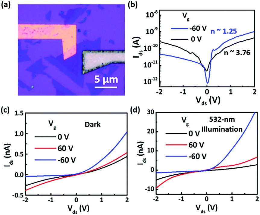 | ||
| Fig. 2 Characterization of the WSe2–MoS2 monolayer device. (a) Optical microscopy images of the WSe2–MoS2 monolayer device. (b) Ids–Vds characteristics of the device under a Vg of 0 V and −60 V. (c and d) Gate-tunable output characteristics of a lateral WSe2–MoS2 heterojunction p–n diode (c) in the dark and (d) under 532 nm laser illumination. | ||
The gate tuning characteristics of the lateral heterojunction device can possibly originate from the electrostatic doping behavior of WSe2.7,19 The CVD-grown WSe2 has been reported as a lightly p-doped semiconductor.24 In contrast to WSe2, MoS2 is normally grown as highly n-doped unintentionally, which makes its Fermi level more resistant to additional electrostatic gating procedures. Therefore, by applying a positive bias, electron doping in WSe2 occurs and WSe2 becomes more intrinsic, and the rectifying behavior becomes less pronounced. When applying a negative bias, hole doping takes place in WSe2, leading to the formation of a heavily p-doped WSe2 region and thus achieving a more ideal p–n junction.
Fig. 3a and b show photoresponse and photovoltaic properties of the lateral heterojunction device. Under 532 nm laser illumination with 2 × 10⁴ W m−2, the device exhibits a 36-fold increase in current with an applied voltage of −2 V, showing the extrordinary photodetection ability of the lateral heterostructure. In this case, the voltage is applied to p-type WSe2 while the n-type MoS2 is grounded. Meanwhile, the open-circuit voltage of 0.3 V and the short-circuit current of 0.51 nA reveal a photovoltaic effect of the device. Fig. 3c shows the reproducibility of the device performance using the lateral monolayer WSe2–MoS2 p–n heterojunction. Fig. 3d and e show the short-time-period photoresponses. The rising time is defined as the time taken to increase from 20% to 80% of the maximum photocurrent, and the falling time is defined as the time taken to decrease from 80% to 20% of the maximum photocurrent, respectively.25 The rising and falling response times of 20 and 30 ms demonstrate its potential for high speed photosensor applications. The response time could be limited by the diffusion time of the laterally connected WSe2 and MoS2 regions, which can be further improved with a better geometry design such as the reduction in device channel length. It is noted that the laser beam diameter is ∼1 mm, which is significantly larger than the active area of the device. In this case, the contact between the metal electrodes and 2D materials would also contribute to the generation of photocurrent. We have previously explored that the Ohmic contact between metal electrodes and 2D materials would lead to a large photoresponse but a longer response time compared with the Schottky-contact devices.26 Therefore, the overall time response may also be limited by the response time at the Ti/MoS2 and Au/WSe2 interfaces. The dynamics of the photogenerated carriers were further evaluated using a mechanical chopper to modulate the frequency of the light source. As shown in Fig. 3f, the lateral heterojunction device can be operated up to 100 Hz modulation frequency. Note that even with the low-resistance contacts used in this study to optimize the photoresponsivity, the p–n junction device has already demonstrated a fast response time potential for fast detection. It is also noted that the gate voltage applied for Fig. 3 is 60 V. We have also measured the photoresponse of the device under the gate voltage of −60 V, as shown in Fig. S2 of the ESI.† The responsivity of the device under a gate voltage of −60 V is very low. This can be attributed to the fact that under a gate voltage of −60 V, the carrier concentration in MoS2 is largely reduced due to the large negative gate bias, leading to a low responsivity. This phenomenon has also been observed in other 2D lateral structures.9
 | ||
| Fig. 3 Photoresponse of the WSe2–MoS2 monolayer device. (a) I–V characteristics of the device in the dark and under 532 nm laser illumination, under −2 V to 2 V biased voltage. (b) Photovoltaic characteristics under 532 nm laser illumination. (c) Time response of the device under 532 nm laser illumination with a bias voltage of −2 V. (d and e) Enlarged (d) rising and (e) falling time response of the device under 532 nm laser illumination with a bias voltage of −2 V. (f) Frequency-dependent photogain of the device under 532 nm laser illumination with a bias voltage of −2 V. | ||
To further characterize the photosensing capability of the device, we measured the responsivity of the lateral heterojunction at various light intensities, AOIs, wavelengths, and operation temperatures. The responsivity is calculated by dividing the measured output current by the illuminating optical power. The actual device area of ∼32 μm2 is estimated from the optical microscopy image shown in Fig. 2a. The actual device area is identified in Fig. S3, and the calculation details are included in the ESI.† As shown in Fig. 4a and b, the lateral heterojunction exhibits excellent omnidirectional light-harvesting properties and its responsivity shows a maximum of 0.26 A W−1 at a light intensity of 500 W m−2, which is >20 times higher than the previously reported results obtained from the vertical heterojunction based on stacked MoS2/WSe2 monolayers.7 In stacked 2D layers, there are additional functional groups, contaminants, or adsorbed gas molecules at the junction interface, which act as the carrier trapping centers and cause severe carrier recombination of the charge carriers in the region. The figure of merit of the lateral heterojunction without any defects in the junction is that the photoexcited carriers could be effectively collected, leading to an excellent device performance, as compared to the vertical heterojunction. The excellent omnidirectional light-harvesting behavior can be attributed to the ultrathin nature and high absorptivity properties of the 2D materials. For conventional photodiodes based on vertical junctions, the responsivity is significantly decreased due to insufficient absorption in the junction area at a certain depth caused by serious light scattering or reflection of the top surface at high AOIs. For example, planar Si-based optical devices have shown more than 90% efficiency reduction when operated under high AOIs (75°) as compared with light being incident normally (0°).13 In contrast, for lateral heterojunction diodes, light can be absorbed from any direction and can directly reach the active area of the device. The maximum responsivity at 500 W m−2 can be attributed to the saturation of photocarriers. For light intensity below 500 W m−2, there are abundant photocarriers available for photogeneration. However, at an intensity above 500 W m−2, most of the charge carriers have been induced in the photogeneration process, resulting in the saturation of the photocarriers and the reduction of responsivity. For most photodetectors, the responsivity is higher at lower light intensities. In our case, the dark current and photocurrent are in the range of 0.1 nA to a few nA. Therefore, at ultralow light intensity, the signal to noise ratio becomes lower and the responsivity calculation may fluctuate depending on the noise level. The decrease of responsivity at a low light power has also been reported in other 2D material photodetectors.26–28 It is worth noting that even at an intensity as low as 50 W m−2, the responsivity of the device remains at 0.12 A W−1, demonstrating extraordinarily high light detectability. The outstanding omnidirectional low-light characteristics enable new indoor applications such as smart homes and intelligent buildings.
 | ||
| Fig. 4 Intensity, angular, wavelength, and temperature dependent photoresponse. (a) Light intensity dependent responsivity of the device under 532 nm laser illumination with a bias voltage of −2 V. (b) AOI-dependent responsivity of the device under 532 nm laser illumination with a bias voltage of −2 V. (c) Responsivity spectrum of the device. (d) Temperature-dependent photo-to-dark current ratio (PDCR) and responsivity of the device under 532 nm laser illumination with a bias voltage of −2 V in a vacuum. | ||
Fig. 4c shows the responsivity spectrum, showing that below 750 nm, WSe2 starts to absorb photons and generate a photocurrent. For a wavelength below 700 nm, more photons can be absorbed both in the WSe2 and MoS2 regions, resulting in a significant increase in responsivity. The results are consistent with the absorption results shown in Fig. 1f. Compared to pure WSe2 and MoS2 films, the improvement of responsivity can be attributed to the following reasons. (1) The lower bandgap of WSe2. Due to the slightly lower bandgap (∼1.35 eV) of WSe2 as compared with MoS2 (∼1.8 eV), more photons above the wavelength of 700 nm can be absorbed in the WSe2 region as compared with the MoS2 films. (2) Higher absorption of MoS2. In Fig. 1f, MoS2 shows a higher absorption below 700 nm. Therefore, the heterojunction can absorb more light at wavelengths below 700 nm to exhibit improved responsivity compared to pure WSe2 films. (3) Defect-free junction quality. For pure 2D-material photodetectors, 2D material films are usually contacted with metal electrodes to form metal–semiconductor–metal Schottky devices. However, the interaction between 2D materials and metals can lead to surface states at the junction interface, giving rise to the enhancement of leakage current. In our device, the lateral heterojunction is almost defect-free and ideal at the p–n interface. Therefore, the dark current under reversed bias can be minimized. Accordingly, the responsivity can be improved due to the combined optical and electrical enhancement. Traditional photodetector devices require high bandgap materials at the top to absorb light with short wavelengths and low bandgap materials at the bottom for long-wavelength light, which increases the cost, complexity, and challenges of device fabrication. By designing lateral heterojunction devices, light with different wavelengths can be successfully absorbed within a single layer of material, which reduces the complexity for device design. It is expected that photosensing devices for a broad range of the wavelength spectrum from the ultraviolet (such as BN) to infrared region (such as graphene) with a variety of combinations can be achieved. Fig. 4d shows that the responsivity of the device remains as high as 0.16 A W−1 at 120 °C under a vacuum, illustrating the capability for high-temperature operation. The device has been kept under a vacuum for high temperature measurements to prevent the oxidation of MoS2 and WSe2. Therefore, the noticeable deterioration in responsivity may be due to the generation of thermal carriers, leading to the increase of dark current, which cannot be eliminated at high temperatures.
Conclusions
In summary, by applying the novel design concept of monolayer lateral p–n heterojunction WSe2–MoS2, we have fabricated an atomically thin photodetector with a high responsivity of 0.26 A W−1, which is 20 times higher than the device based on van der Waals heterojunctions. Since the lateral p–n junction is formed via direct epitaxial growth, the junction is clean and without photon quenching sites as in stacked van der Waals junctions. An outstanding omnidirectional light harvesting behavior has also been achieved and characterized to show the ability to retain high responsivity even at large AOIs, which is unachievable using the traditional top-down structural design. In addition, low-light detectability with a maximum responsivity at 500 W m−2 and a high-temperature operation up to 120 °C have been achieved. These unique and intriguing properties pave a way for the future development of sub-nano semiconductor devices and applications.References
- D. S. Tsai, K. K. Liu, D. H. Lien, M. L. Tsai, C. F. Kang, C. A. Lin, L. J. Li and J. H. He, ACS Nano, 2013, 7, 3905–3911 CrossRef CAS PubMed.
- D. S. Tsai, D. H. Lien, M. L. Tsai, S. H. Su, K. M. Chen, J. J. Ke, Y. C. Yu, L. J. Li and J. H. He, IEEE J. Sel. Top. Quantum Electron., 2014, 20, 3800206 Search PubMed.
- M. L. Tsai, S. H. Su, J. K. Chang, D. S. Tsai, C. H. Chen, C. I. Wu, L. J. Li, L. J. Chen and J. H. He, ACS Nano, 2014, 8, 8317–8322 CrossRef CAS PubMed.
- T. Roy, M. Tosun, J. S. Kang, A. B. Sachid, S. B. Desai, M. Hettick, C. C. Hu and A. Javey, ACS Nano, 2014, 8, 6259–6264 CrossRef CAS PubMed.
- B. Radisavljevic, A. Radenovic, J. Brivio, V. Giacometti and A. Kis, Nat. Nanotechnol., 2011, 6, 147–150 CrossRef CAS PubMed.
- M. H. Chiu, M. Y. Li, W. Zhang, W. T. Hsu, W. H. Chang, M. Terrones, H. Terrones and L. J. Li, ACS Nano, 2014, 8, 9649–9656 CrossRef CAS PubMed.
- M. M. Furchi, A. Pospischil, F. Libisch, J. Burgdörfer and T. Mueller, Nano Lett., 2014, 14, 4785–4791 CrossRef CAS PubMed.
- R. Cheng, D. Li, H. Zhou, C. Wang, A. Yin, S. Jiang, Y. Liu, Y. Chen, Y. Huang and X. Duan, Nano Lett., 2014, 14, 5590–5597 CrossRef CAS PubMed.
- X. Duan, C. Wang, J. C. Shaw, R. Cheng, Y. Chen, H. Li, X. Wu, Y. Tang, Q. Zhang, A. Pan, J. Jiang, R. Yu, Y. Huang and X. Duan, Nat. Nanotechnol., 2014, 9, 1024–1030 CrossRef CAS PubMed.
- C. Huang, S. Wu, A. M. Sanchez, J. J. P. Peters, R. Beanland, J. S. Ross, P. Rivera, W. Yao, D. H. Cobden and X. Xu, Nat. Mater., 2014, 13, 1096–1101 CrossRef CAS PubMed.
- M. Y. Li, Y. Shi, C. C. Cheng, L. S. Lu, Y. C. Lin, H. L. Tang, M. L. Tsai, C. W. Chu, K. H. Wei, J. H. He, W. H. Chang, K. Suenaga and L. J. Li, Science, 2015, 349, 524–528 CrossRef CAS PubMed.
- Y. Y. Zhang, J. Zhang, G. Luo, X. Zhou, G. Y. Xie, T. Zhu and Z. F. Liu, Nanotechnology, 2005, 16, 422–428 CrossRef CAS.
- W. R. Wei, M. L. Tsai, S. T. Ho, S. H. Tai, C. R. Ho, S. H. Tsai, C. W. Liu, R. J. Chung and J. H. He, Nano Lett., 2013, 13, 3658–3663 CrossRef CAS PubMed.
- G. J. Lin, H. P. Wang, D. H. Lien, P. H. Fu, H. C. Chang, C. H. Ho, C. A. Lin, K. Y. Lai and J. H. He, Nano Energy, 2014, 6, 36–43 CrossRef CAS.
- T. Aytug, A. R. Lupini, G. E. Jellison, P. C. Joshi, I. H. Ivanov, T. Liu, P. Wang, R. Menon, R. M. Trejo, E. Lara-Curzio, S. R. Hunter and J. T. Simpson, J. Mater. Chem. C, 2015, 3, 5440–5449 RSC.
- H. P. Wang, K. T. Tsai, K. Y. Lai, T. C. Wei, Y. L. Wang and J. H. He, Opt. Express, 2012, 20, A94–A103 CrossRef CAS PubMed.
- M. Bernardi, M. Palummo and J. C. Grossman, Nano Lett., 2013, 13, 3664–3670 CrossRef CAS PubMed.
- L. Y. Gan, Q. Zhang, Y. Cheng and U. Schwingenschlögl, J. Phys. Chem. Lett., 2014, 5, 1445–1449 CrossRef CAS PubMed.
- K. F. Mak, C. Lee, J. Hone, H. Shan and T. F. Heinz, Phys. Rev. Lett., 2010, 105, 136805 CrossRef PubMed.
- J. S. Ross, P. Klement, A. M. Jones, N. J. Ghimire, J. Yan, D. G. Mandrus, K. Taniguchi, K. Watanabe, K. Kitamura, W. Yao, D. H. Cobden and X. Xu, Nat. Nanotechnol., 2014, 9, 268–272 CrossRef CAS PubMed.
- Y. Y. Hui, X. Liu, W. Jie, N. Y. Chan, J. Hao, Y. T. Hsu, L. J. Li, W. Guo and S. P. Lau, ACS Nano, 2013, 7, 7126–7131 CrossRef CAS PubMed.
- W. Zhao, Z. Ghorannevis, K. K. Amara, J. R. Pang, M. Toh, X. Zhang, C. Kloc, P. H. Tan and G. Eda, Nanoscale, 2013, 5, 9677–9683 RSC.
- S. Xiao, P. Xiao, X. Zhang, D. Yan, X. Gu, F. Qin, Z. Ni, Z. J. Han and K. K. Ostrikov, Sci. Rep., 2016, 6, 19945 CrossRef CAS PubMed.
- J. K. Huang, J. Pu, C. L. Hsu, M. H. Chiu, Z. Y. Juang, Y. H. Chang, W. H. Chang, Y. Iwasa, T. Takenobu and L. J. Li, ACS Nano, 2014, 8, 923–930 CrossRef CAS PubMed.
- C. DeCusatis and C. J. S. DeCausatis, Fiber Optic Essentials, Academic Press, 2005 Search PubMed.
- W. Zhang, M. H. Chiu, C. H. Chen, W. Chen, L. J. Li and A. T. S. Wee, ACS Nano, 2014, 8, 8653–8661 CrossRef CAS PubMed.
- X. Sun, C. Qiu, J. Wu, H. Zhou, T. Pan, J. Mao, X. Yin, R. Liu, W. Gao, Z. Fang and Y. Su, Opt. Express, 2015, 23, 25209–25216 CrossRef PubMed.
- S. Mukherjee, R. Maiti, A. K. Katiyar, S. Das and S. K. Ray, Sci. Rep., 2016, 6, 29016 CrossRef CAS PubMed.
Footnote |
| † Electronic supplementary information (ESI) available. See DOI: 10.1039/c6nh00075d |
| This journal is © The Royal Society of Chemistry 2017 |