
 Open Access Article
 This Open Access Article is licensed under a Creative Commons Attribution-Non Commercial 3.0 Unported Licence
Pursuing the tribovoltaic effect for direct-current triboelectric nanogenerators
Chong
Xu
ab,
Jinran
Yu
ab,
Ziwei
Huo
ab,
Yifei
Wang
ab,
Qijun
Sun
 *abc and
Zhong Lin
Wang
*ad
*abc and
Zhong Lin
Wang
*ad
aBeijing Institute of Nanoenergy and Nanosystems, Chinese Academy of Sciences, Beijing, 101400, China. E-mail: sunqijun@binn.cas.cn; zhong.wang@mse.gatech.edu
bSchool of Nanoscience and Technology, University of Chinese Academy of Sciences, Beijing, 100049, China
cCenter on Nanoenergy Research, School of Physical Science and Technology, Guangxi University, Nanning, 530004, China
dGeorgia Institute of Technology, Atlanta, Georgia 30332-0245, USA
First published on 3rd February 2023
Abstract
The shortage of fossil energy and global climate change have driven humankind to find a new type of renewable, accessible, and clean energy. The triboelectric nanogenerator (TENG) is a new energy technology relying on the coupling of triboelectrification and electrostatic induction. To alleviate the issues of low current density and requirements for complex management circuits, direct-current triboelectric nanogenerators (DC-TENGs) based on the tribovoltaic effect have emerged, exhibiting DC output signals with higher current density and simpler structure design. In this review, the development progress and microscopic mechanisms of DC-TENGs based on the tribovoltaic effect are elaborately summarized for the first time, which is of great significance for designing high-performance DC-TENGs and advancing energy-harvesting technology. The reported DC-TENGs are scientifically classified and the corresponding working mechanisms are explained in detail. The output performances of different types of devices are systematically compared from the aspects of current density, peak power density, open-circuit voltage, short-circuit current, peak power output, and internal resistance. Furthermore, this review delivers a constructive discussion on how to improve the output performance from three perspectives, namely, materials and structures, external parameters, and multiple energy harvesting strategies. Finally, the potential application fields and development prospects of DC-TENGs are discussed. It is expected that the diversified DC-TENGs will bring about revolutionary development in high-efficiency energy harvesting and broaden the applications in intelligent IoTs.
Broader contextThe shortage of fossil energy and global climate change have driven humankind to find a new type of renewable, accessible, and clean energy. The triboelectric nanogenerator (TENG) is a new energy technology relying on the coupling of triboelectrification and electrostatic induction. To alleviate the issues of low current density and requirements for complex management circuits, direct-current triboelectric nanogenerators (DC-TENGs) based on the tribovoltaic effect have emerged, exhibiting DC output signals with higher current density and simpler structure design. In this review, the development progress and microscopic mechanisms of DC-TENGs based on the tribovoltaic effect are elaborately summarized for the first time, which is of great significance for designing high-performance DC-TENGs and advancing energy-harvesting technology. The reported DC-TENGs are scientifically classified and the corresponding working mechanisms are explained in detail. The output performances of different types of devices are systematically compared from the aspects of current density, peak power density, open-circuit voltage, short-circuit current, peak power output, and internal resistance. Furthermore, this review delivers a constructive discussion on how to improve the output performance from three perspectives, namely, materials and structures, external parameters, and energy coupling strategies. Finally, the potential application fields and development prospects of DC-TENGs are discussed. |
1. Introduction
Energy is the basis for human survival and the main driver for the development of a sustainable economic society. Throughout the past 200 years of the development of modern industrial society, coal, petroleum, and other fossil fuels have remained the main energy resources consumed by human civilization. However, since fossil energy resources will be in short supply and eventually exhausted in the future, current energy utilization and economic development models have hit the bottleneck. In addition, the large-scale development and utilization of fossil fuels have led to excessive emissions of greenhouse gases, which are considered as the trigger for a series of major environmental problems such as global warming, extreme weather, and environmental degradation.1 Therefore, considering the shortage of fossil energy and global climate change, it is urgent to find a new type of renewable, distributed, and clean energy. The triboelectric nanogenerator (TENG) is an emerging novel energy technology that combines triboelectrification and electrostatic induction and can effectively convert high-entropy and low-frequency mechanical energy (i.e., random and weak mechanical energy from the surroundings) into electrical energy. As a renewable and clean energy source, TENGs are very competitive due to their simple structure, light weight, low cost, and diverse material choices. Hence, they have great potential to power distributed devices or to be integrated in self-powered systems.2–4 Conventional TENGs can readily convert frictional energy into electrical energy by generating alternating current (AC), but their low current density and the requirement for rectification remain the major limitations.5,6 Analogous to the photovoltaic effect, Wang's group has proposed the tribovoltaic effect.7 Once a P-type semiconductor slides on an N-type semiconductor, the newly formed atomic bond at the interface releases an energy quantum, named “bindington”, which excites electron–hole pairs at the PN junction. The electrons and holes are separated by the internal built-in electric field at the PN junction, generating a direct current. Based on the tribovoltaic effect, direct-current triboelectric nanogenerators (DC-TENGs) that can output a DC signal with a simpler structure and higher current density have been developed and are expected to be a new type of semiconductor energy technology with high power density.8,9Fig. 1 schematically shows a comparison between the conventional AC-TENG and DC-TENG (based on the tribovoltaic effect, note that the DC-TENG based on air breakdown is not included in this review) with the main focus on DC-TENGs from the aspects of material, structure, working mechanism, output performance, decisive parameters, and applications.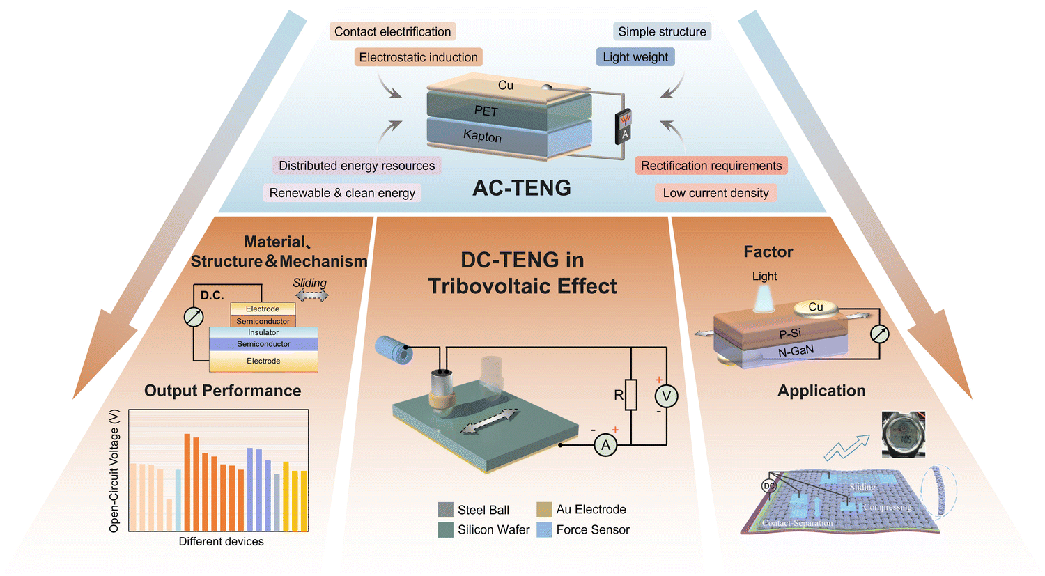 | ||
| Fig. 1 Schematic illustration of the AC-TENG and DC-TENG based on the tribovoltaic effect. | ||
Conventional AC-TENGs and DC-TENGs have different frictional materials, structures, working mechanisms, and typical signal characteristics. In conventional TENGs, the current output in the AC form is generated by the vertical or horizontal movement between two contact materials with opposite polarities (Fig. 2a).5 The frictional materials are usually made of organic insulating polymers.10 The working mechanism of the AC-TENG can be described as follows. When two materials with different electron affinities come into contact, electrostatic induction occurs at the contact interface. Then electrons are driven to flow through the external circuit when the two materials separate from each other (Fig. 2b),11 thereby generating an AC signal due to the periodic contact–separation process (Fig. 2c).4,12–15 In contrast, DC-TENGs can generate an output current in the form of a DC by rubbing one semiconductor against another semiconductor (or metal) (Fig. 2d). The mechanism is that the frictional energy released by atomic bond formation excites the charge carriers (electron–hole pairs in the semiconductor or dynamic electrons in the metal) at the sliding interface, and these charge carriers are directionally separated under the built-in electric field.10 Another study reports that there is also an interfacial electric field on the surface that dominates the transport of charge carriers (Fig. 2e),16–18 and the DC signal is generated under the synergetic effect of the built-in electric field and interfacial electric field (Fig. 2f), which is similar to the current generation process by the photovoltaic effect.19 Accordingly, this effect for DC-TENGs (discussed in this review) is called the tribovoltaic effect. In recent years, DC-TENGs have been intensively developed since 2018.20Fig. 3 shows the timeline of milestones of DC-TENGs based on the tribovoltaic effect. Typical DC-TENGs are selected according to the active materials and device structures. The representative device reported in 2018 was a metal–insulator–semiconductor point contact DC-TENG; afterwards, a graphene/metal-Si heterostructure device was developed in 2019; then, a metal–semiconductor sliding system with a simplified structure was reported in 2020; in 2021, a more sophisticated device structure was developed based on the polarized water driven dynamic PN junction; afterwards, more semiconductor heterojunctions (e.g., GaN–Si) were proposed to significantly boost the output performance. In the future, more durable materials and optimized device structures should be considered to pursue high performance DC-TENGs for practical applications. Sophisticated devices with customizable properties and deep understanding of the working mechanism of the tribovoltaic effect are also highly encouraged (Fig. 3).10,17,20–22 The reported DC-TENGs can effectively convert mechanical energy directly into constant DC energy, which is more suitable for charging energy storage devices, powering portable electronics, or directly driving distributed sensors for the Internet of Things (IoTs).8,17,18,21–24 However, to the best of our knowledge, there are no review reports that systematically and comprehensively elaborate on DC-TENGs based on the tribovoltaic effect in terms of mechanism, material/structure, performance, external parameters, applications, etc.
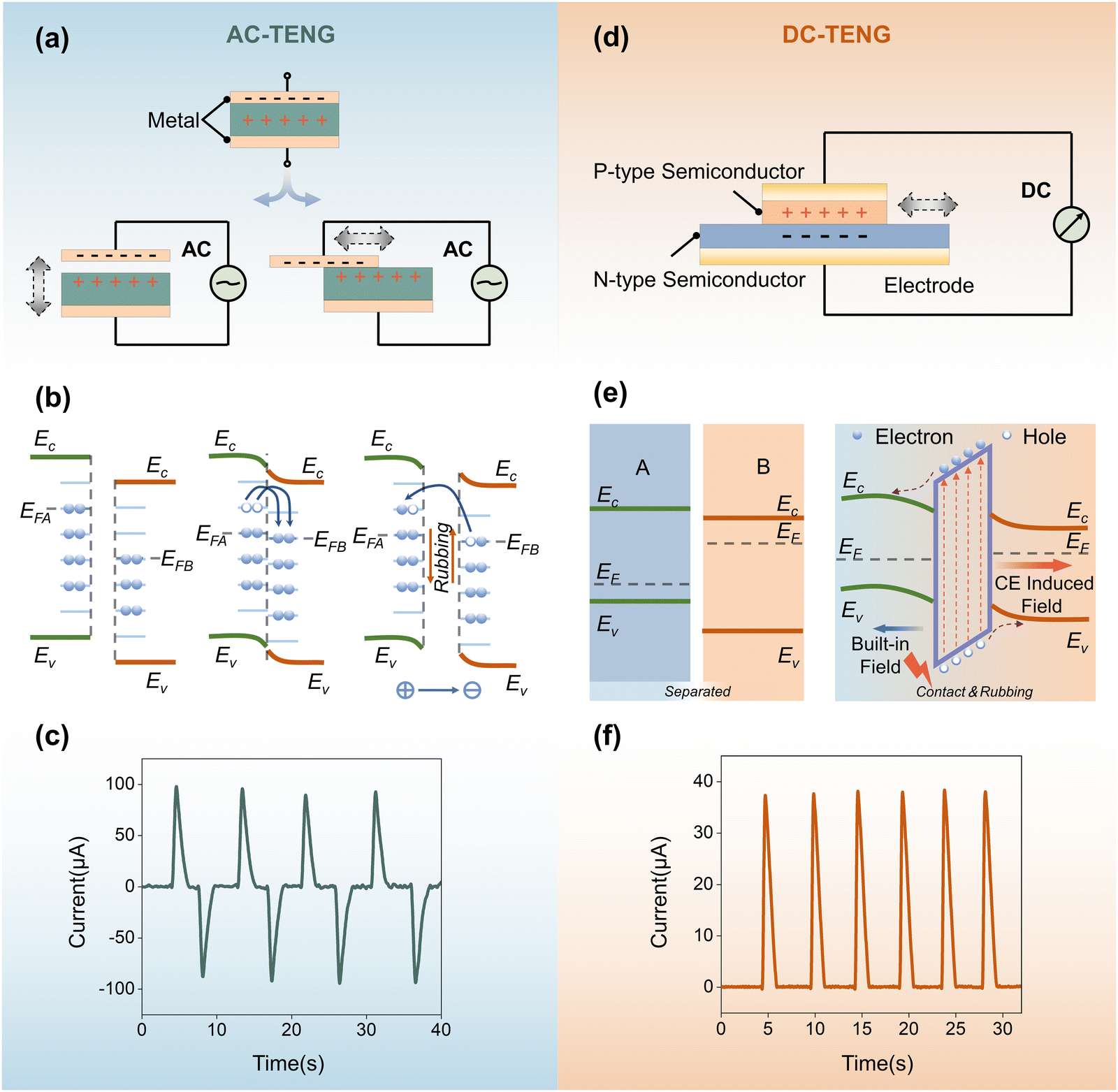 | ||
| Fig. 2 Comparison between the AC-TENG and DC-TENG based on the tribovoltaic effect. (a) Vertical contact-separation mode and lateral-sliding mode of the AC-TENG. (b) Working mechanism of the AC-TENG. (c) Basic electrical characteristics of the AC-TENG. (d) Device structure of the DC-TENG based on the tribovoltaic effect. (e) Working mechanism of the DC-TENG based on the tribovoltaic effect. (f) Basic electrical characteristics of the DC-TENG based on the tribovoltaic effect. | ||
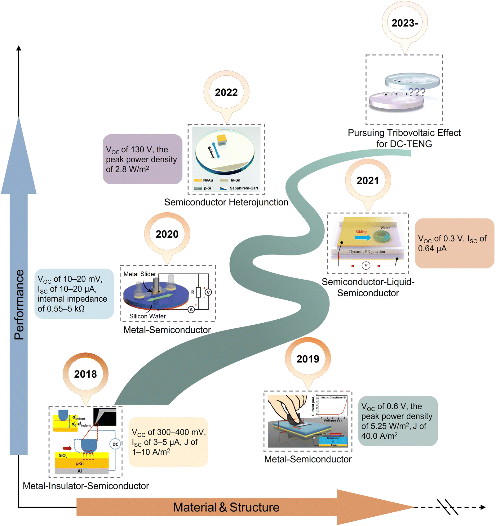 | ||
| Fig. 3 Timeline of milestones of DC-TENGs based on the tribovoltaic effect. Reproduced with permission from ref. 20. Copyright 2018 Elsevier Ltd. Reproduced with permission from ref. 22. Copyright 2019 Wiley-VCH Verlag GmbH & Co. KGaA, Weinheim. Reproduced with permission from ref. 10. Copyright 2020 Wiley-VCH Verlag GmbH & Co. KGaA, Weinheim. Reproduced with permission from ref. 21. Copyright 2021 AAAS. Reproduced with permission from ref. 17. Copyright 2022 The Royal Society of Chemistry. | ||
In this review, DC-TENGs based on the tribovoltaic effect are scientifically classified into six categories according to the different materials and structures, i.e., metal–semiconductor (M–S) contact devices, metal–insulator–semiconductor (M–I–S) contact devices, semiconductor–semiconductor (S–S) contact devices, semiconductor–insulator–semiconductor (S–I–S) contact devices, liquid–semiconductor (L–S) contact devices, and metal/semiconductor–liquid–semiconductor (M/S–L–S) contact devices. First, the underlying microscopic mechanisms of DC-TENGs are explained, followed by the individual mechanism of each type of device. Then, the output performances of different types of devices are compared in terms of current density, peak power density, open-circuit voltage, short-circuit current, peak power output, and internal resistance. After that, possible strategies to improve the output performance of DC-TENGs are provided from the perspectives of materials and structures, external parameters, and multiple energy harvesting strategies. Specifically, material and structure improvement can be implemented by selecting different solid materials, different dielectric layers, or different liquid materials with relevant device structures; the crucial parameters include frictional speed, load pressure, external impedance, etc.; the multiple energy harvesting strategies mainly cover the energy coupling in DC-TENGs (e.g., coupling between mechanical and photonic/thermal energy) and multisource device-driving strategies (e.g., by wind energy). Finally, the potential significant applications of DC-TENGs are discussed in consideration of future challenges and development.
2. Microscopic mechanisms of DC-TENGs based on the tribovoltaic effect
To explore the origin of DC output from contact-sliding on semiconductors, the mechanism of the tribovoltaic effect needs to be investigated from a microscopic perspective. Atomic force microscopy (AFM), with a high spatial resolution, is frequently used to observe the charge transfer between materials, offering a significant tool to study the principles of triboelectric electrification at the nanoscale. In addition, conductive-AFM (C-AFM) is capable of measuring the electric current flow between the tip and the sample, allowing the study of charge carrier transport at the contact interfaces of metal–semiconductor or semiconductor–semiconductor structures in DC-TENGs.25–28As shown in Fig. 4a(i), by sliding the conductive platinum/iridium-coated (Pt/Ir-coated) silicon AFM tip over few-layer molybdenum disulfide (MoS2, synthesized by pulsed laser deposition, PLD) on a silver coated SiO2/Si substrate, direct electron excitation occurs at the metal–semiconductor interface accompanied by the diffusion-drift of charge carriers across the contact interface. And the nonequilibrium carrier transport is enhanced by the strong local electric fields at the conductive nanoscale tips, which will lead to a very high current density.29Fig. 4a(ii) shows the AFM topographic images of three adjacent MoS2 crystal grains identified as 1, 2, and 3, respectively. Different MoS2 grain surfaces have different surface potential fluctuations, indicating different triboelectric-excited current responses. Fig. 4a(iii) displays the C-AFM current–voltage (I–V) characteristic curves of grain 1. It is evident from the C-AFM I–V spectra that grain 1 exhibits diode rectification characteristics, suggesting that the rectified Schottky barrier at the tip–sample interface plays a key role in outputting DC.5
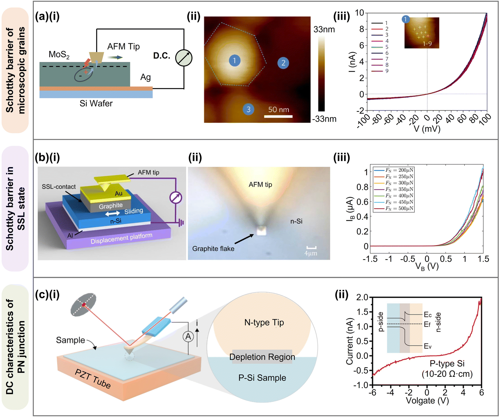 | ||
| Fig. 4 Microscopic mechanisms of DC-TENGs based on the tribovoltaic effect. (a) Schematic diagram (i), AFM image (ii), and I–V curves (iii) of conductive Pt/Ir-coated AFM tip sliding on MoS2 thin film. Modified with permission from ref. 5. Copyright 2017 Springer Nature. (b) Schematic diagram (i), optical image (ii), and I–V curves (iii) of superlubric microsized graphite flakes sliding on the N–Si surface. Reproduced with permission from ref. 9. Copyright 2021 Springer Nature. (c) Schematic diagram (i) and I–V curve (ii) of the N-type semiconductor tip sliding on the surface of the P–Si sample. Reproduced with permission from ref. 19. Copyright 2020 Wiley-VCH Verlag GmbH & Co. KGaA, Weinheim. | ||
There may also be another mechanism of current generation in sliding Schottky junctions, (i.e., the mechanism of depletion layer establishment and destruction, DLED), which can be verified with a specific microscale Schottky superlubric generator (SSG). As shown in Fig. 4b(i), the sliding junction is established with a structural superlubricity (SSL) state, which is an ultralow friction and wearless state between the two sliding-contact solid surfaces of microsized graphite flakes and N-type silicon (N–Si).30 The graphite flakes are transferred to a smooth surface of N–Si with a certain doping concentration, and the backside of N–Si is coated with an Al electrode. Using an Au-coated C-AFM tip to press against the top of the graphite flakes, the lateral sliding between the superlubricated graphite surface and the smooth N–Si surface is controlled by the underlying displacement platform. Fig. 4b(ii) is an optical microscopic image of the graphite/N–Si SSG. Due to the work function difference between the graphite flakes and N–Si, electrons will transfer between their contact surfaces and lead to the formation of a depletion layer and a Schottky barrier in the equilibrium state. Fig. 4b(iii) shows the I–V characteristic curves under different normal forces,9 which display typical rectification characteristics at the contact interface between graphite and N–Si.
In addition to the DC characteristics of sliding Schottky junctions, the PN junctions also show DC characteristics. As shown in Fig. 4c(i), a DC signal is generated by sliding an N-type semiconductor tip on the surface of the P-type Si sample using C-AFM. The N-type semiconductor is a nitrogen-doped diamond-coated tip with good resistance to abrasion, and the P-type samples are boron (or phosphorus) doped silicon with different resistivities. During the rubbing process, the current between the tip and the sample is recorded by using the C-AFM instrument. As the silicon sample is P-type doped, there will be the formation of a PN junction due to the diffusion of electrons from the tip to the Si at the sliding contact interface. Fig. 4c(ii) shows the I–V characteristic curves based on the diamond-coated tip contacting the P–Si sample (10–20 Ω cm), which also represent the rectification characteristics at the interface between the tip and the sample. The results suggest that when the tip contacts the P–Si sample, a PN heterojunction is formed at the interface with a built-in electric field. As the silicon samples are processed by inductively coupled plasma reactive ion etching (ICP-RIE), the density of states can be readily increased by doping or introducing defects on the semiconductor surfaces.31,32 In addition, the triboelectric current characterized during the two semiconductor sliding process also increases with the load pressure.19
All the above results indicate that the triboelectric current can be readily induced by the tribovoltaic effect in two steps. In the first step, electron–hole pairs at the sliding interface are excited by the released energy during mechanical friction, which can be explained by the electronic transitions between surface states during contact or bond formation on the sliding interface. In the second step, the electron–hole pairs at the sliding interface are separated by the built-in electric field at the Schottky junction or PN/NN heterojunction, resulting in a triboelectric current output (similar to the current output due to the photovoltaic effect).5,9,19,33
3. Categories of DC-TENGs and the corresponding working mechanisms
Various DC-TENGs based on the tribovoltaic effect have been reported based on different materials and device structures, and the relevant working mechanisms are also slightly different. The main factors affecting the mechanisms among the reported devices are material choice and structural design. Accordingly, DC-TENGs can be classified into six categories according to the selected materials and device structures, including metal–semiconductor contact devices, metal–insulator–semiconductor contact devices, semiconductor–semiconductor contact devices, semiconductor–insulator–semiconductor contact devices, liquid–semiconductor contact devices, and metal/semiconductor–liquid–semiconductor contact devices. Depending on whether there is an insulator layer (as a dielectric layer), the relevant working mechanisms and different types of DC-TENGs are schematically illustrated in Fig. 5 (the details are discussed in the following).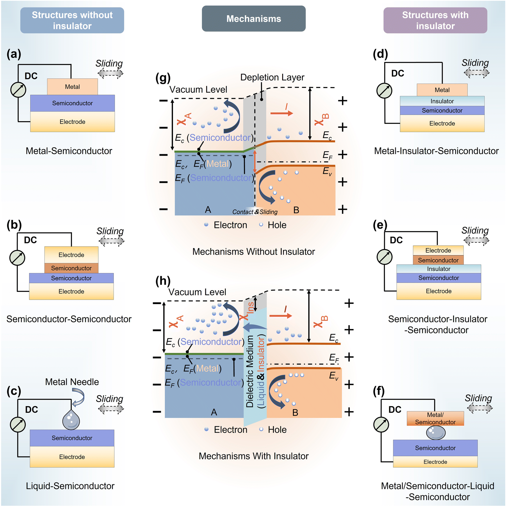 | ||
| Fig. 5 Six categories of DC-TENGs and the corresponding working mechanisms. (a) Metal–semiconductor (M–S) contact devices. (b) Semiconductor–semiconductor (S–S) contact devices. (c) Liquid–semiconductor (L–S) contact devices. (d) Metal–insulator–semiconductor (M–I–S) contact devices. (e) Semiconductor–insulator–semiconductor (S–I–S) contact devices. (f) Metal/semiconductor–liquid–semiconductor (M/S–L–S) contact devices. Working mechanisms of the DC-TENG (g) without a dielectric layer and (h) with a dielectric layer. | ||
3.1 Devices with solid–solid contacts without an insulator as a dielectric layer: PN type
Fig. 5a and g display the Schottky junction (also known as the metal–semiconductor junction) and the relevant working mechanism. In this case, lateral sliding between the metal and the semiconductor will lead to the formation of atomic bonds. During this process, the released energy can be absorbed to excite nonequilibrium electron–hole pairs, which are separated by the built-in electric field, accumulated to induce a potential difference at the interface, and lead to the output voltage and current through the external circuit.34 More specifically, when the metal and semiconductor are in contact, a depletion layer is immediately formed at the heterojunction interface. When the metal slides on the semiconductor (without changing the contact area), the back-end depletion layer will gradually disappear and the front-end depletion layer will be dynamically reconstructed. The dynamic appearance/disappearance of the depletion layer disrupts the distribution of the electrostatic charge carriers, accelerates/confines the electrons and holes diffused in the depletion layer, and leads to the separation of drifting electrons and holes. The separation direction of electron–hole pairs depends on the direction of the as-determined built-in electric field during the sliding process, thus resulting in the DC signal output.22As shown in Fig. 5b and g, the semiconductor–semiconductor interface forms a dynamic heterojunction or homojunction. When one semiconductor slides on the other semiconductor with different Fermi levels, the electron–hole pairs at the sliding interface are excited by the released energy during the friction process (this released energy may originate from the electronic transitions between different surfaces during the contact process, or during the formation of bonds at the sliding interfaces).19 Subsequently, the excited electron–hole pairs are separated by the built-in electric field at the heterojunction or homojunction, resulting in a triboelectric current output. A more specific process can be explained as follows: when the two semiconductors come into contact, a depletion layer is immediately formed at the heterojunction or homojunction interface. Then the two semiconductors slide against each other without changing the contact area, which leads to the dynamic destruction and creation of a depletion layer, breaks the balance between the drift and diffusion currents, and causes the diffusing carriers to separate under the influence of the built-in electric field.8 The output current direction generated by carrier separation is determined by the direction of the built-in electric field in the heterojunction or homojunction at the contact surface, which is not affected by the relative sliding direction. In addition, the direction of the built-in electric field also depends on the Fermi level of the two semiconductors instead of the external mechanical motion, so the output from the semiconductor–semiconductor contact device is also a DC signal.11
3.2 Devices with solid–solid contact with an insulator as the dielectric layer: PiN type
The native thin oxide layer (∼1.6 nm) on the silicon surface provides a pathway for triboelectrification induced electrons to enter the silicon substrate through quantum mechanical tunneling. In other words, electrons are still conducted in the semiconductor through the thin oxide layer under the ultrahigh interfacial electric field due to the tunneling and hopping effect (Fig. 5h). According to the quantum mechanical tunneling effect, the triboelectric current decays exponentially with the increasing thickness of the deposited oxide layer.20 Therefore, by inserting a dielectric layer into the DC-TENG (Fig. 5d and e), the device output can be finely tuned and enhanced due to the energy level difference between the valence band of the semiconductor and the conduction band of the dielectric layer.8,243.3 Liquid–solid contact devices
The tribovoltaic effect can also occur at the liquid–semiconductor interface, which is first studied by sliding water droplets on the semiconductor surface to verify the mechanism. When sliding deionized water droplets on the surface of a Si substrate with different doping types or concentrations (Fig. 5c), both the triboelectric voltage and current output directions are found to depend on the built-in electric field at the liquid–solid interface (assuming that the EF of substance B in Fig. 5g is the “Fermi level” of ionized water). This phenomenon indicates that the liquid–solid contact induced triboelectric outputs are caused by the tribovoltaic effect. When the water molecules slide on the semiconductor surface, the electron–hole pairs are first excited by the energy released during the molecular bonding process and then separated by the built-in electric field at the sliding interface, thus leading to the DC output signal. This experiment confirms for the first time the existence of electron transfer at the liquid–solid interface. More importantly, a “two-step” model is proposed for the formation process of electric double layers (EDLs), i.e., the first step of electron transfer between the liquid and the solid and the second step of chemical/physical adsorption of ions.35–383.4 Metal/semiconductor–liquid–solid contact devices
A schematic illustration of the metal/semiconductor–liquid–solid contact device structure is shown in Fig. 5f (note that the dielectric medium in the figure is liquid for this type of device). The liquid material acts as a moving dielectric medium and slides between the metal and the semiconductor (or between semiconductor and semiconductor) with different Fermi levels. Then it is dynamically polarized and results in a continuous DC output. Specifically, when a water molecule is in contact with two solid materials, the sandwiched water molecule is instantly polarized due to the Fermi level difference between the metal and the semiconductor (or between semiconductor and semiconductor). The free charge carriers in the solid accumulate at the liquid–solid interface, thereby achieving electrostatic equilibrium and polarization equilibrium. As the droplet moves, the equilibrium between the polarization-induced diffusion and drift currents is repeatedly broken and recreated.39 At the same time, these polarization-induced electrons and holes are released and bounce onto the solids on both sides, respectively, so a continuous DC voltage or current is generated in the external circuit. The direction of the direct current output depends on the Fermi level difference of the metal and semiconductor (or semiconductor and semiconductor),21 and the direction and magnitude of the voltage are determined by the ΔEF between the two solid materials. Therefore, the outputs can be readily modulated based on the sandwich structure.394. Typical output parameters of DC-TENGs
In recent years, the output performance of DC-TENGs based on various materials and device structures has been continuously improved. A complete review of the output performances and elaborate evaluation of related parameters among different DC-TENGs will greatly facilitate the precise selection of active materials, inspire sophisticated design of preferential device structures, and boost the output performance in future research. Regarding the main purpose of DC-TENGs in energy harvesting, typical output parameters are correspondingly extracted from the reported literature, including current density, peak power density, open-circuit voltage, short-circuit current, peak power output, internal resistance, etc. The DC-TENG based on the tribovoltaic effect has many advantages over other types of nanogenerators. For instance, it has been reported that DC-TENGs exhibit ultrahigh current density, which is approximately 103 times higher than that of conventional TENGs and approximately 104 times higher than that of piezoelectric nanogenerators.40,41 The internal impedance (∼kΩ) of a dynamic semiconductor homojunction DC-TENG is quite low compared to the impedance (∼MΩ) of polymer-based nanogenerators, but matches the impedance (∼kΩ) of semiconductor-based information electronics (promising for future integration with general semiconductor devices).42Fig. 6 in detail evaluates various DC-TENG devices based on six different parameters, including current density,5,8–10,16,18,20,22,24,43–45 peak power density,5,8,9,16–18,22,24,43–46 open-circuit voltage,5,8,16,18,20,21,24,34,35,39,44,47–49 short-circuit current,5,8,10,11,16,18,20,21,24,34,35,39,47,48,50–52 peak power output,8,9,11,20,24,35,47–51 and internal resistance.8,10,11,18,20,24,39,44,47–51 Based on the elaborate comparison shown in Fig. 6, it can be observed that, by introducing a dielectric layer, the metal–semiconductor and semiconductor–semiconductor contact devices appear with correspondingly increased current density and peak power density due to the increase in the potential barrier (Fig. 6a and b). The overall open-circuit voltage of semiconductor–semiconductor contact devices is higher than that of metal–semiconductor and liquid–semiconductor devices (Fig. 6c). The semiconductor–liquid–semiconductor sandwich structure device is more competitive in current and voltage output than the liquid–semiconductor device (Fig. 6c and d). The peak power output depends on the contact area and power density of the device, while the internal resistance is only related to the geometric parameters and the resistivity of the material itself (a smaller material resistivity generally leads to a smaller internal resistance) (Fig. 6e and f).10,42,44 In brief, the detailed evaluation indicates that different choices of materials and structures affect the performance of DC-TENGs belonging to the same category. If different metal materials and semiconductor materials are selected, the output performance of the device can be significantly different.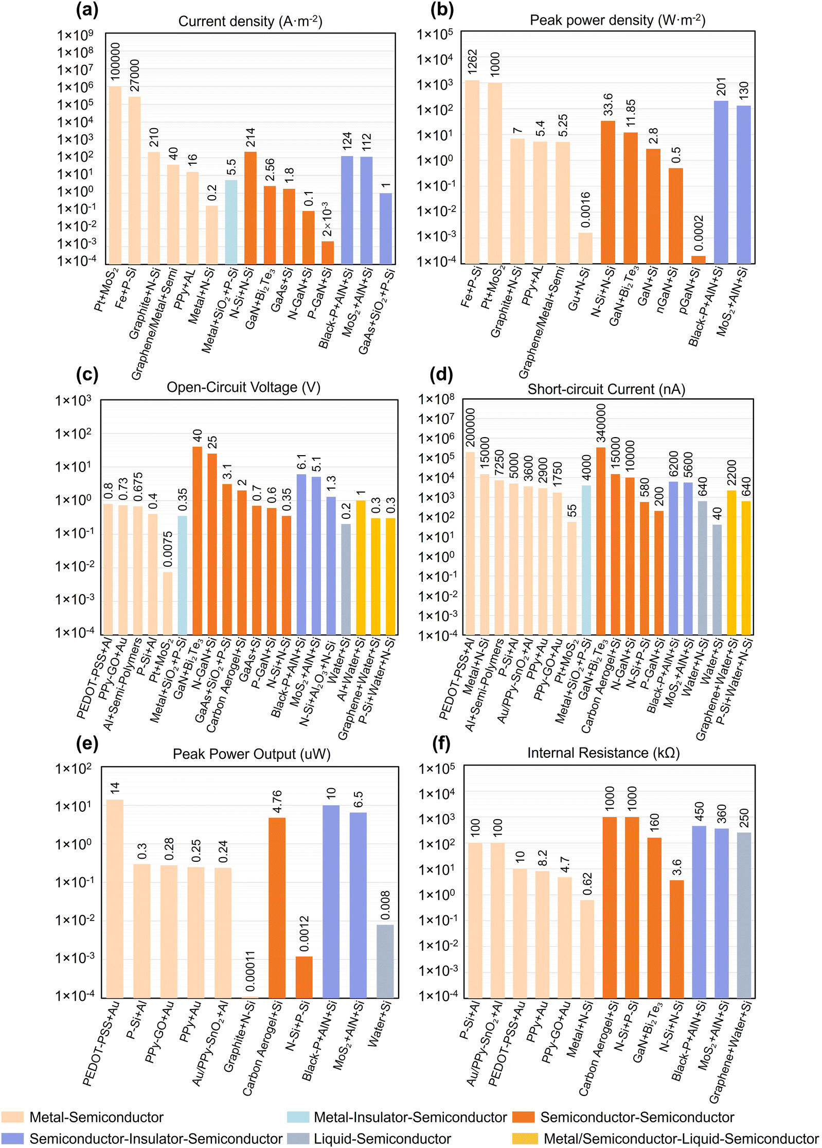 | ||
| Fig. 6 Output parameters of DC-TENGs. (a) Current density.5,8–10,16,18,20,22,24,43–45 (b) Peak power density.5,8,9,16–18,22,24,43–46 (c) Open-circuit voltage.5,8,16,18,20,21,24,34,35,39,44,47–49 (d) Short-circuit current.5,8,10,11,16,18,20,21,24,34,35,39,47,48,50–52 (e) Peak power output.8,9,11,20,24,35,47–51 (f) Internal resistance.8,10,11,18,20,24,39,44,47–51 | ||
According to the above discussions, the factors that can affect the output of the DC-TENG are summarized according to the extent of direct influence on device performance or the capacity for optimizing the output performance. Based on the working mechanisms and output performances of different DC-TENGs, three main factors affecting the device output are generalized from the aspects of materials and device structures, external parameters, and the energy coupling strategy. The effect of materials and structures is discussed based on metal and semiconductor materials, dielectric layer materials, liquid materials, and device structures; external parameters include frictional speed, load pressure, external impedance, etc.; an energy coupling strategy is involved in the coupling with photonic energy, thermal energy, and wind energy. Detailed discussions on the factors affecting DC-TENGs will be presented in the following three sections.
5. Internal affecting factors: materials and device structures
5.1 Metals
The work functions of the reported metal materials in the metal–semiconductor contact DC-TENGs range from 2.14 to 5.90 eV (Fig. 7a(i)),53–57 which directly determine the direction and magnitude of the voltage output. For example, as shown in Fig. 7b, when an Au (5.10 eV) or Al (4.28 eV) electrode is placed against the semiconductor N–Si (4.34 eV) to construct a DC-TENG, the electrons will transfer in different directions under the built-in electric field and result in different voltage output directions. In addition, the work function difference between the metal and the semiconductor determines the relative surface potential difference and affects the magnitude of the voltage output. It is concluded that the voltage direction depends on the positive and negative signs of ΔEF and that the voltage magnitude is proportional to the absolute value of ΔEF (|ΔEF|).39 It is worth noting that the device durability and flexibility can be significantly improved by changing the metal material into graphene due to its higher conductivity, flexibility, and durability, allowing the device to slide back and forth tens of thousands times.22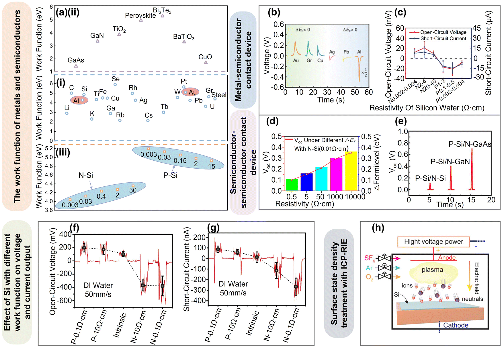 | ||
| Fig. 7 Internal affecting factors: materials and device structures. (a) Work functions of (i) different metals, (ii) semiconductors, and (iii) silicon wafers with different doping types and resistivities.53–65 (b and c) Output performances of M–S contact devices with different (b) metals and (c) semiconductors. Reproduced with permission from ref. 39. Copyright 2021 American Chemical Society. Reproduced with permission from ref. 10. Copyright 2020 Wiley-VCH Verlag GmbH & Co. KGaA, Weinheim. (d) Output performances and Fermi level differences of the S–S homojunction with different resistivities. Reproduced with permission from ref. 44. Copyright 2020 AAAS. (e) Output performances of S–S heterojunctions with different semiconductors. Reproduced with permission from ref. 8. Copyright 2019 Elsevier Ltd. (f and g) Open-circuit voltage (f) and short-circuit current (g) of L–S contact devices with different resistivities. Reproduced with permission from ref. 35. Copyright 2020 Elsevier Ltd. (h) Schematic diagram of ICP-RIE treatment of silicon wafers. Reproduced with permission from ref. 19. Copyright 2020 Wiley-VCH Verlag GmbH & Co. KGaA, Weinheim. | ||
5.2 Semiconductors
The work functions of different semiconductors vary with the doping types and doping concentrations. Even the same type of semiconductor material with different resistivities has shown different work functions.58 The work functions of different semiconductors utilized in the reported DC-TENGs are summarized and displayed in Fig. 7a(ii) and (iii).59–65 The work function of the semiconductor in DC-TENGs affects the internal resistance, short-circuit current, and open-circuit voltage. Generally, different doping types determines the resistivity in semiconductor materials, in which higher resistivity will result in higher internal resistance in the DC-TENG. In addition, the work function of the semiconductor is calculated according to the resistivity and doping conditions, which is also correlated with the resistivity to affect the built-in electric field strength in the DC-TENG. In addition, a small work function difference between the two contact materials in the DC-TENG will lead to decreased built-in electric field strength and nonequilibrium carrier drift velocity. The consequently lowered Schottky barrier will cause more charges to pass through the Schottky barrier to form a drift current and affect both the short-circuit current and the open-circuit voltage (Fig. 7c).10 The output voltages depend on the Fermi level differences in both homojunction devices (Fig. 7d) and heterojunction devices (Fig. 7e).8,44 Specifically, even when deionized water contacts with silicon in different doping states, the resultant variations in the work function difference will lead to different built-in electric fields and have significant influences on the output voltage and current (Fig. 7f and g).35In addition to the doping concentrations and doping types, the surface states also impact on the output performance of DC-TENGs. Surface treatment of the semiconductor layer promises DC-TENGs with higher output performance. For instance, Q. Zhang et al. immersed a silicon wafer in HF solution for 1 min to etch away the possible oxide layers on both sides. This treatment can minimize the influence of adsorption contamination, barrier height of the contact interface, and interface state.66 Therefore, the output performances of the P–Si and N–Si electrode pair are improved after this simple surface treatment.67 Another example is to treat silicon wafers with ICP-RIE as shown in Fig. 7h, which can significantly increase the surface state density of semiconductors by doping or introducing defects on their surface and lead to the increment of current density as a consequence.19,31,32 Another study indicates that when the metal tip (Fe) slides on a smooth and rough silicon wafer, the rough interface will induce a higher leakage current and current density. This is attributed to the Fermi level pinning effect at the high surface state of the rough interface causing more charge carriers to bounce back. In addition, changing the surface state of semiconductors also provides a good way to achieve ultrahigh current density DC-TENGs.43
5.3 Dielectric layers
For the metal–insulator–semiconductor or semiconductor–insulator–semiconductor DC-TENG, the electrons can tunnel through the insulating layer during the fiction process and result in triboelectric output with high current density.20,44 In this type of DC-TENG, both the material type and thickness of the dielectric layers can influence the output current and voltage, the mechanism of which is mainly related to the height of the enhanced interfacial barrier.8,24,44,68,69 For example, in the metal–insulator–semiconductor DC-TENG, the output current decreases with the increasing thickness of the SiOx dielectric layer. The reason is that the wave function ψ of electrons decays exponentially within the potential barrier, while the probability that the electrons can tunnel through the potential barrier is limited (Fig. 8a).20 In contrast, the output voltage is often positively correlated with the height of the potential barrier. With the same dielectric layer, the height of the potential barrier increases with the increasing thickness of the insulator, which will lead to an increased output voltage. With different dielectric layers, the average output voltage is positively correlated with the barrier height of the interfacial barrier between the semiconductor and the dielectric layer (Fig. 8b).70–72Fig. 8c shows one-dimensional band alignment of conduction and valence band edges for the semiconductors (Si) and various dielectric layers (e.g., graphene, AlN, HfO2, ZnO, Al2O3, SiO2, black phosphorus).8,24,44 Different dielectric layers can be selected on demand according to the required output performances.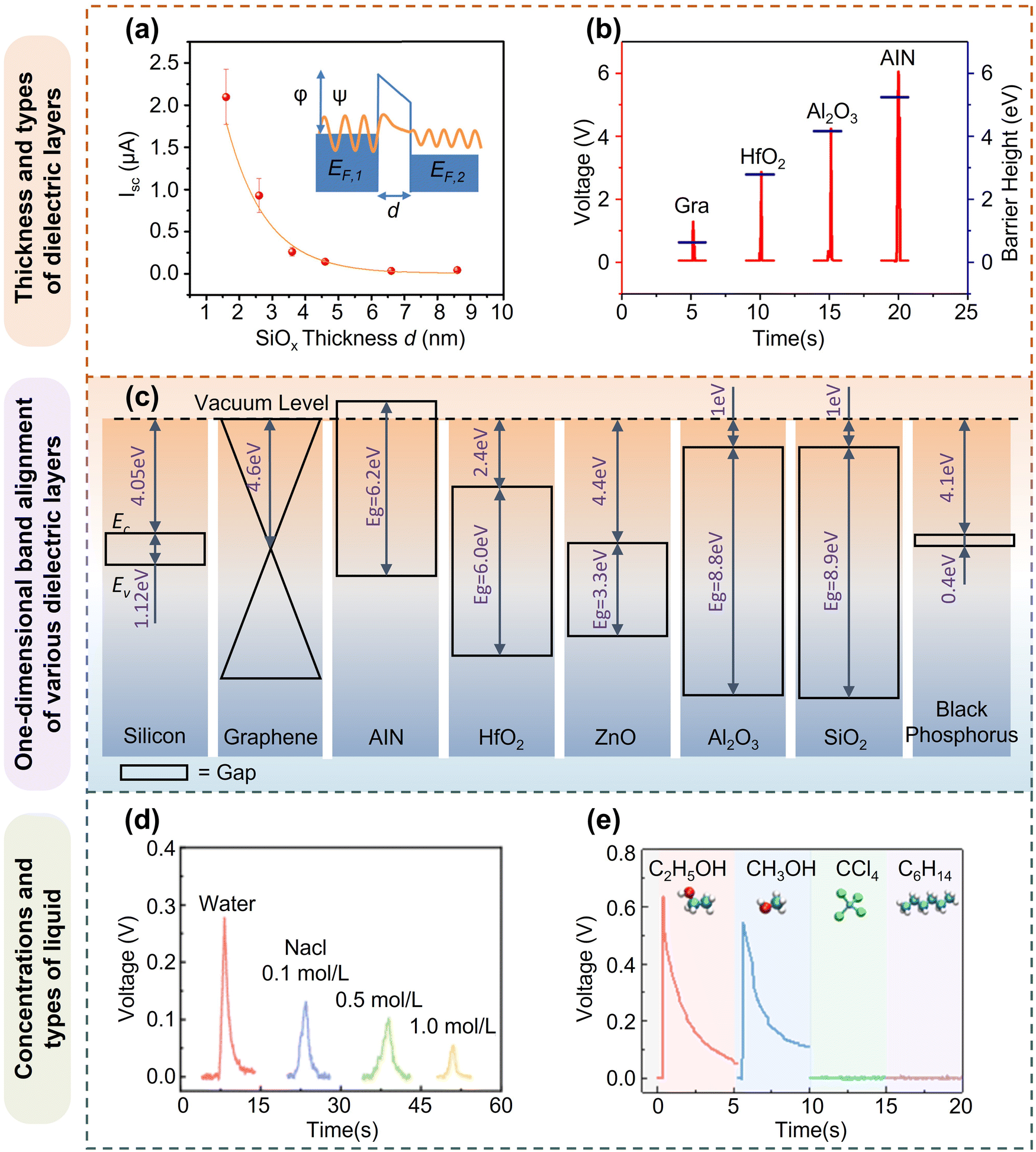 | ||
| Fig. 8 Effect of dielectric layers and liquid materials on output performance. (a) ISC with different SiOx thicknesses in M–I–S point contact systems. Reproduced with permission from ref. 20. Copyright 2018 Elsevier Ltd. (b) VOC and barrier height with different dielectric layers in the S–I–S contact device. Reproduced with permission from ref. 24. Copyright 2019 AAAS. (c) One-dimensional band alignment of conduction and valence band edges for various dielectric layers and semiconductors.8,24,44 (d) VOC of P–Si (0.1 Ω cm) and NaCl solution contact devices with different NaCl concentrations. Reproduced with permission from ref. 35. Copyright 2020 Elsevier Ltd. (e) VOC of the S–L–S contact devices with polar and nonpolar liquids. Reproduced with permission from ref. 21. Copyright 2021 AAAS. | ||
In addition, D. Yang et al. have added polyalphaolefin SpectraSyn 4 as a lubricant in the oxide dielectric layer to realize rectified Schottky contact between the steel ball and N–Si, exhibiting a reduced coefficient of friction from 0.76 to 0.16.73 After 20![[thin space (1/6-em)]](https://www.rsc.org/images/entities/char_2009.gif) 000 reciprocating sliding cycles, the wear loss can be significantly reduced by 99.5% while still maintaining a nearly constant DC output. From the dynamic I–V characteristic curve, it can be observed that the presence of the lubricating oil film significantly enhances the rectified Schottky barrier between the steel ball and N–Si, yet slightly curbs the VOC and ISC. This result suggests that the employment of lubricants can significantly reduce the wear of the device without weakening the tribovoltaic effect at the metal–lubricant–semiconductor interface. This may inspire more studies in the future to improve the wear resistance of semiconductor-based DC-TENGs.
000 reciprocating sliding cycles, the wear loss can be significantly reduced by 99.5% while still maintaining a nearly constant DC output. From the dynamic I–V characteristic curve, it can be observed that the presence of the lubricating oil film significantly enhances the rectified Schottky barrier between the steel ball and N–Si, yet slightly curbs the VOC and ISC. This result suggests that the employment of lubricants can significantly reduce the wear of the device without weakening the tribovoltaic effect at the metal–lubricant–semiconductor interface. This may inspire more studies in the future to improve the wear resistance of semiconductor-based DC-TENGs.
5.4 Liquid materials
One of the benefits of choosing liquid materials as the friction layer is that they can also effectively minimize wear and tear. The salt concentrations, liquid types, and polarities are all found to readily influence the tribovoltaic effect.21,35,39 Different liquid materials can also lead to different electron transitions and bond interactions at the liquid–solid interface. As shown in Fig. 8d, the positive triboelectric voltage (i.e., VOC) decreases with increasing NaCl concentration in the DC-TENG based on P–Si (0.1 Ω cm) and NaCl solutions at different concentrations. This VOC decrement is not caused by the change in the built-in electric field but by the reduction in the number of electron–hole pairs generated at the interface.35 In addition, the output voltages of the DC-TENG based on semiconductor–liquid–semiconductor contact are different depending on the polarity of the utilized liquids, e.g., the nonpolar liquid of C6H14 and the polar liquid of water, C2H5OH, or (CH2OH)2. As shown in Fig. 8e, the DC-TENG based on n-hexane (C6H14) and other nonpolar liquids cannot produce any voltage output. The key to electrical output is the dynamic polarization of water (or other polarized liquids), which is related to the dielectric constant (bearing an inversely proportional relationship with the voltage output). Therefore, the semiconductor–C2H5OH–semiconductor device shows the best performance.215.5 Structures
DC-TENGs based on the tribovoltaic effect have various structures as shown in Fig. 9a–f, such as sliding structure,11 needle tip structure,43 rotating structure,8 interlayer structure,39 rolling structure,16 and sphere-plane structure.73 Among these structures, the sliding structure in Fig. 9a is the most common.11 The tip structure involves devices that adopt linear reciprocating sliding of the metal tip on the semiconductor planar structure. Fig. 9b shows the sliding of the Fe tip on rough P–Si that achieves an ultrahigh power density of 1262 W m−2. When the needle slides on a rough silicon surface with many defects, the current output increases significantly, confirming the effect of the surface state on the output power.43 Another study reports that linear sliding enables an exceptionally high current density (106 A m−2) with DC outputs, which is attributed to the nonequilibrium carrier transport enhanced by the strong local electric field at the nanoscale tip.29 Apart from linear sliding, a circular rotational motion is also available on the semiconductor plane to prepare the DC-TENG.20 As shown in Fig. 9c, the planar structure of the P-type semiconductor/N-type semiconductor device allows both linear reciprocating motion and circular rotating motion. However, the output voltages are different in the two modes (pulsed voltage outputs for the linear reciprocating mode and continuous voltage outputs up to 3.1 V for the cyclic rotating mode).8 A typical example of a DC-TENG based on the interlayer structure of graphene–water–semiconductor is shown in Fig. 9d. The dynamically polarized water–semiconductor interfaces can induce DC output signals regardless of the droplet moving directions. The open-circuit voltage can be adjusted by the Fermi level difference between the two plates sandwiching the water droplets. The rolling mode is shown in Fig. 9e to compare with the sliding modes based on the N-GaN/Al DC-TENGs. The voltage and current outputs for the sliding mode (0.28 V and 0.25 μA) are much higher than that of the rolling mode (0.05 V and 8 nA). The sliding mode of the GaN/Al DC-TENG can harvest more frictional energy, indicating that mechanical friction is the main driving force of carrier excitation.16 The new type of sphere-plane structured DC-TENG has been designed and reported more recently (Fig. 9f), in which the metal–semiconductor heterojunction in the sphere-plane mode can lead to high electrical output and low wear rate.73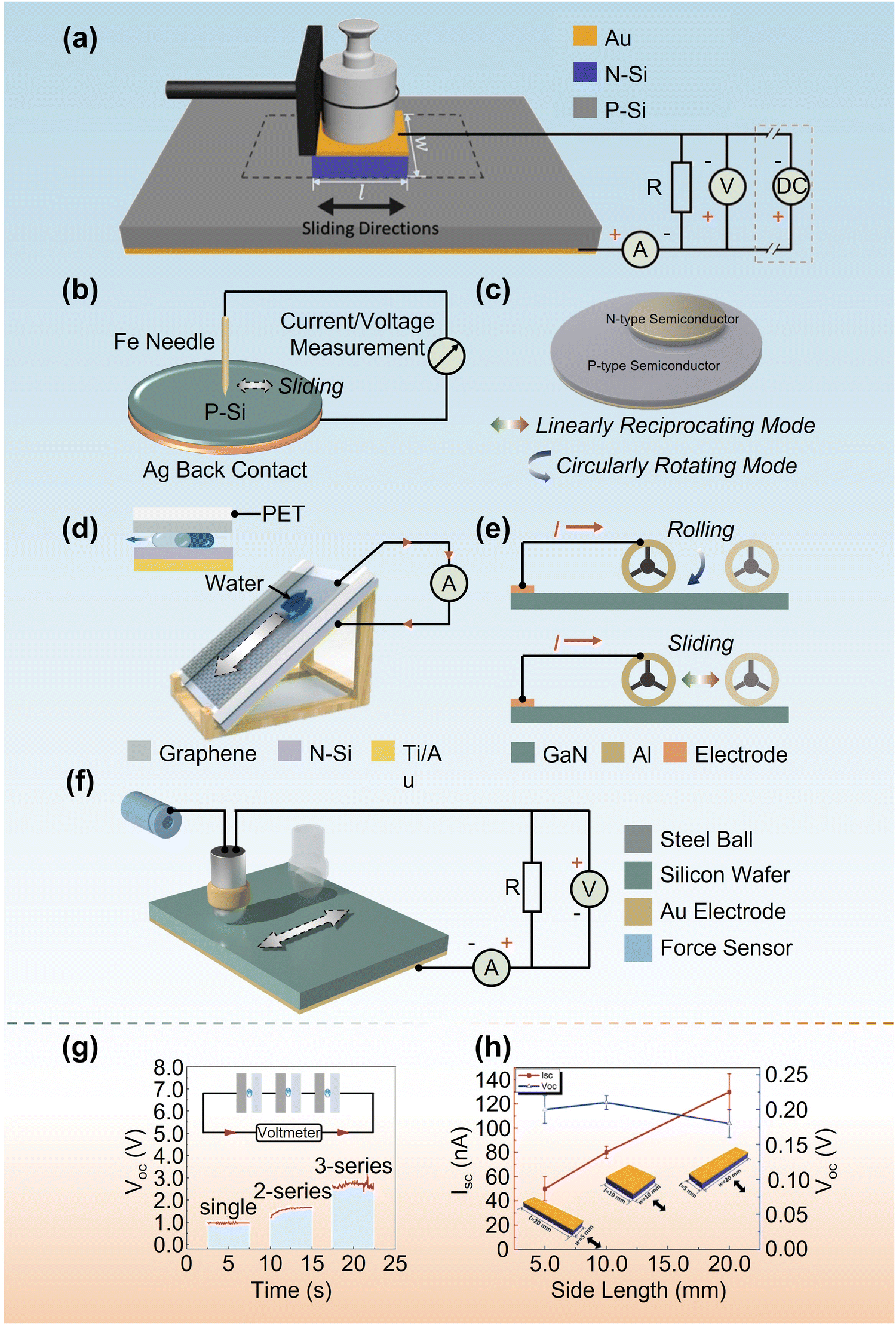 | ||
| Fig. 9 Schematic diagrams of different DC-TENGs. (a) Sliding structure. Modified with permission from ref. 11. Copyright 2019 Elsevier Ltd. (b) Needle tip structure. Modified with permission from ref. 43. Copyright 2019 Wiley-VCH Verlag GmbH & Co. KGaA, Weinheim. (c) Rotating structure. Modified with permission from ref. 8. Copyright 2019 Elsevier Ltd. (d) Sandwich structure. Modified with permission from ref. 39. Copyright 2021 American Chemical Society. (e) Rolling structure. Modified with permission from ref. 16. Copyright 2022 American Chemical Society. (f) Sphere structure. Modified with permission from ref. 73. Copyright 2022 Elsevier Ltd. (g) VOC with different numbers of series in the aluminum–water–silicon contact device. Reproduced with permission from ref. 39. Copyright 2021 American Chemical Society. (h) ISC and VOC with different sliding lengths. Reproduced with permission from ref. 11. Copyright 2019 Elsevier Ltd. | ||
Connecting multiple DC-TENGs in series or parallel is also an effective approach to improving the output performance. One packaged DC-TENG based on aluminum–water–silicon can output a voltage of 1.0 V. Three devices in series can result in a higher output voltage of 2.7 V (Fig. 9g).39 The connected DC-TENGs can be more readily used for sustainable, reliable, and portable power supply compared with a single liquid–solid DC-TENG, which is commonly reported to suffer from discontinuous water replenishment, low AC voltage output, dielectric material degradation, and low adaptability.74–76 In addition, another way to improve the output performance of the DC-TENG is to change the device size, e.g., the length of the sliding side. As shown in Fig. 9h, the three top electrodes in DC-TENGs have the sliding sides of different lengths (maintain the same contact area). Larger lengths lead to higher ISC but barely influence VOC. This result can be attributed to the following reason. During the top electrode sliding process under the same contact pressure and sliding speed, the newly created PN junctions at the front and the previous PN junctions that disappear at the back will be larger for devices with larger side lengths. As only the new overlapping/released regions can effectively facilitate charge transfer, this result will induce more electrons and holes.11
In brief, contact materials with a larger Fermi level difference, an available dielectric layer with an increased barrier height, an appropriate liquid material, and the optimal device structure should be taken into consideration for designing DC-TENGs with high output. By customizing the utilized materials and device structures for the DC-TENG, the output voltage/current and internal resistance can be effectively controlled to optimize the final power output.10 Compared with piezoelectric NGs and traditional TENGs, DC-TENGs based on the tribovoltaic effect can efficiently generate DC output and quickly charge capacitors without rectification circuits. Optimizing the above internal affecting factors can significantly reinforce the applications of DC-TENGs in the field of energy harvesting.44
6. External affecting factors
We have conducted a comprehensive statistical analysis on the research related to DC-TENGs released in recent years, which suggests that the main external factors affecting DC-TENGs are frictional speed or acceleration, contact area of the interface (or volume of the droplet), load pressure, external impedance, temperature, etc.Frictional speed or acceleration
Generally, when the friction speed or acceleration increases, the output voltage/current will also increase and reach a saturation state (Fig. 10a). For example, it is reported that the deionized water droplets sliding on a P–Si wafer (0.1 Ω cm) at a speed of 20 mm s−1 lead to a VOC of ∼200 mV, while sliding at a speed of 50 mm s−1 increases the VOC close to 400 mV after 200 cycles of sliding.35 However, in some cases, it is also possible that the output voltage barely changes.11,17,21,22,24,34,35 Additionally, at a given speed, transient sliding can induce current output more efficiently than constant sliding,11i.e., instantaneous sliding with larger acceleration results in higher current.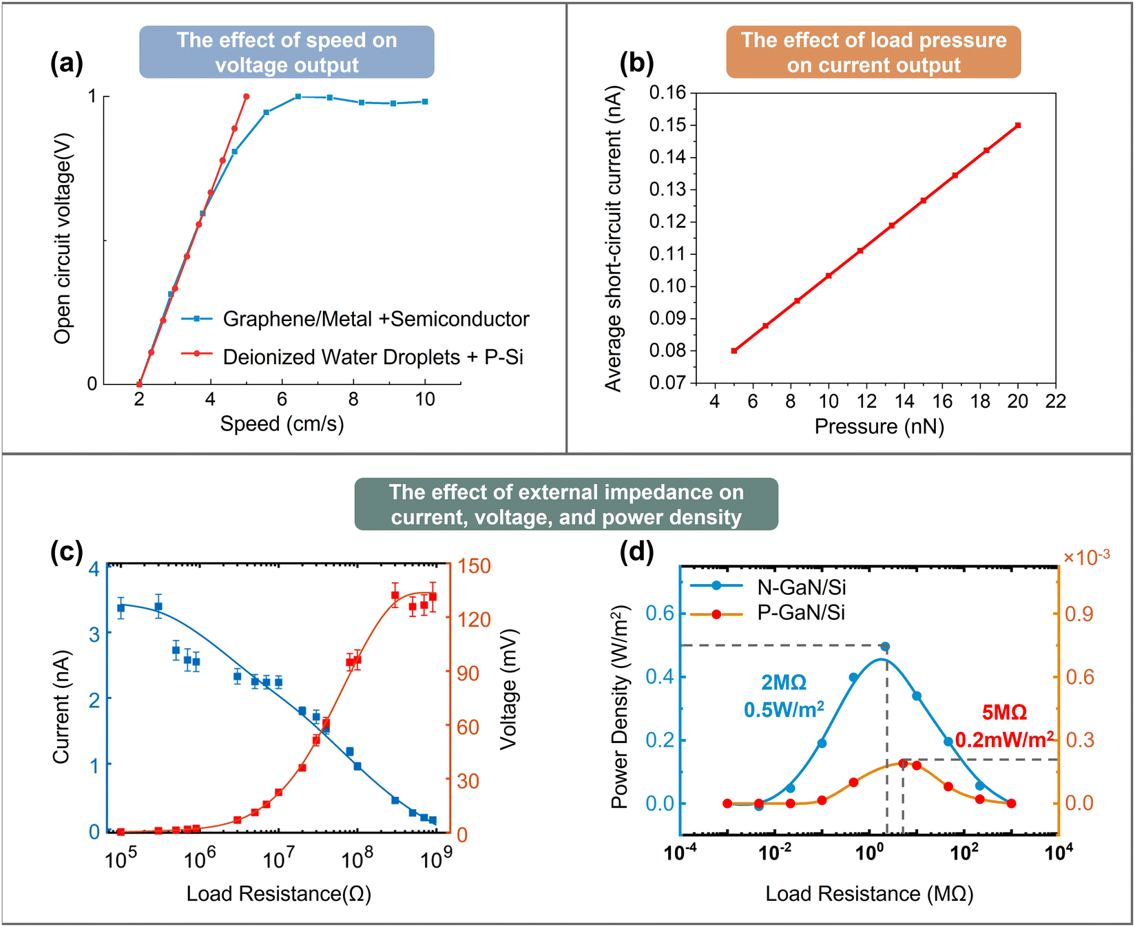 | ||
| Fig. 10 External affecting factors. (a) VOC with different sliding speeds of the M–S and L–S contact devices. (b) ISC with different load pressures of the DC-TENG. (c) ISC and VOC with different external impedances of the DC-TENG. Reproduced with permission from ref. 9. Copyright 2021 Springer Nature. (d) Impedance matching curves of DC-TENGs with different heterojunctions. Modified with permission from ref. 16. Copyright 2022 American Chemical Society. | ||
Contact area of the interface (or volume of the droplet)
The output current of the DC-TENG is reported to be linear with the metal area in metal/silicon Schottky diodes,10,22 the contact area in dynamic P–Si/N-GaAs TENGs,8 or the static contact diameters for deionized water and P–Si.35 However, the power density and internal resistance decrease with increasing contact area,10 while the current density remains almost constant with a small contact area.8 For the liquid–solid DC-TENG (e.g., semiconductor–water–semiconductor contact device), a larger water volume results in greater current output under a constant moving speed of the silicon wafer. However, the voltage output is basically unchanged since it is determined by the Fermi level difference between the two semiconductors.21Load pressure
Experimental results show that the increased load pressure (F) imposed on the DC-TENG enables a nearly linear increase in ISC output (Fig. 10b), which will also increase the amount of transferred charges and VOC.8,9,11,16,19,24,34,73 The reason is that a larger F will lead to a higher interfacial electric field and more excited charge carriers.16,19 Another report also suggests that the probable current fluctuation may be related to the stick-slip behavior caused by the microscopic friction fluctuation (related to the change in the frictional force under different sliding states).11 For graphene/silicon Schottky diodes, a larger load pressure is necessary, and the optimal pressure for graphene is evaluated to be 5 N when the diode reaches the best rectification characteristics.22 However, it has been reported in some special cases that, when the metal tip contacts the semiconductor, the power density is independent of pressure and velocity, while the efficiency (η, defined as Pout/Pin) is negatively correlated with pressure and velocity. This indicates that when the pressure and velocity exceed the limit, the extra power inputs cannot be efficiently converted into electrical energy due to the gradually saturated rebounding centers for the charge carriers. In addition, there are more chances for the recombination of electron–hole pairs at high speed.43 However, it has been reported that the peak power density in the metal–semiconductor contact device increases with pressure and speed,10 which may be explained by its larger contact surface imposing more influence on the power density.External impedance
When a DC-TENG is connected to an external impedance (R), in most cases, VOC will increase with larger R, while ISC and current density will decrease (Fig. 10c).9 Accordingly, the peak value of the power density can be extracted at a certain value of R, which is close to the internal resistance (r) of the DC-TENG.8–10,17,20–22,24,43,44,73 The impedance matching curves of the DC-TENG with two different heterojunctions are shown in Fig. 10d, in which the curves are obtained by fitting the statistical experimental data.16 The output power density of the device based on the N-GaN/Si heterojunction reaches the maximum value of 0.5 W m−2 with an external impedance of 2 MΩ; the device based on P-GaN/Si has a maximum output power density of 0.2 mW m−2 with an external impedance of 5 MΩ. In addition, under the external impedance of 6 MΩ, the power density of the N-GaN/Si-TENG is improved to approximately 1 mW m−2. Compared with the highest voltage output of other DC-TENGs,8,22,24,44,47,77,78 the VOC of the N-GaN/Si device increases fourfold.16Temperature
A DC-TENG with a dynamic van der Waals Schottky junction can operate at extremely low temperatures with increased voltage/current output. This can be explained by the accumulation of electrons and holes due to the surge in mobility and the mean free path at lower temperatures.23 The literature report shows that the current of the PN junction decreases with increasing operating temperature.11 When the temperature rises, the Fermi level in the two semiconductors moves toward the center of the band gap, resulting in a decreased built-in potential and current output. For the tribovoltaic effect at the interface of deionized water and N–Si/P–Si, a higher temperature tends to boost the triboelectric voltage/current output, which is attributed to the decreased contact angle between silicon and water under the increased temperature. However, for the interface between the NaOH solution and N–Si, the triboelectric current tends to increase with increasing temperature. However, the triboelectric voltage according to the temperature is also closely related to the pH value of the liquid materials.38Humidity
In previous research, it is reported that the influence of humidity on the performance of DC-TENGs is almost negligible.8,16,18,39,73 Recently, a humidity-enhanced tribovoltaic DC-TENG (relative humidity (RH) = 90%) was demonstrated with ∼88 times higher transferred charges and ∼100 times higher peak power compared to that in the low humidity state (RH = 30%), which can be attributed to the coupling effect of the enhanced surface state and reduced contact resistance. This research provides an effective method to boost the output performance of DC-TENGs, presenting the great potential of DC-TENGs for energy-harvesting applications in a high humidity environment (e.g., oceans, rain, etc.).46In brief, the influence of external factors on DC-TENGs can be represented as follows. First, higher frictional speed and larger load pressure can increase the output voltage. Second, higher frictional speed, larger contact area, and larger load pressure can increase the current output. Third, higher frictional speed, smaller contact area, and larger load pressure can improve the peak power density.43
7. Multiple energy harvesting and the mechanisms
Multiple energy harvesting includes energy coupling and multisource device-driving strategies (e.g., wind energy driving). Thereinto, the energy coupling strategy is further divided into energy coupling of mechanical/photonic energy and mechanical/thermal energy.7.1 Photonic energy
As shown in Fig. 11a, the DC-TENG based on the PN junction of P–Si/N-GaN can be modulated by UV light to enhance the output. Under irradiation with UV light at 365 nm and 28 mW cm−2, the ISC value is 154 nA and the VOC value is 3.35 V. Compared with the results in the dark environment, the current output increases 13 times and the voltage output increases 4 times under UV light irradiation.79 These results can be explained by the wide-bandgap semiconductor of GaN (band gap is ∼3.4 eV), which has a fixed absorption band for ultraviolet light, high electron drift velocity, and good chemical and mechanical stability.80 After irradiation with ultraviolet light, both the carrier concentration and the triboelectric output can be increased. The corresponding working mechanism is illustrated in Fig. 11g and h. When P–Si slides on N-GaN (Fig. 11g), the thermal equilibrium in the PN junction is disrupted with electron transition from the N-region (with a high Fermi energy level) to the P-region (with a low Fermi energy level). The Fermi energy level of the N-type semiconductor moves downward and the Fermi energy level of the P-type semiconductor moves upward, eventually forming a unified Fermi energy level in the PN junction. At the same time, the conduction and valence bands in the P- and N-regions become bent. When UV light is irradiated on the PN junction, photons excite more electron–hole pairs at the PN junction interface (Fig. 11h). This optical enhancement effect is not a simple superposition between mechanical energy-induced bound back carriers and photogenerated carriers but a nonlinear optical enhancement effect, in which the photogenerated electrons and holes induced in the light absorption region are scattered and accelerated by the bound back electrons and holes in the depletion region, respectively. This optical enhancement effect results in a higher current density, which can provide a feasible way to increase the power conversion efficiency of nanogenerators and improve the output current for self-powered sensing.79,81 A higher optical power density, faster friction speed and acceleration, larger P–Si resistivity, and larger contact area of the PN junction can all enhance the triboelectric output.79,82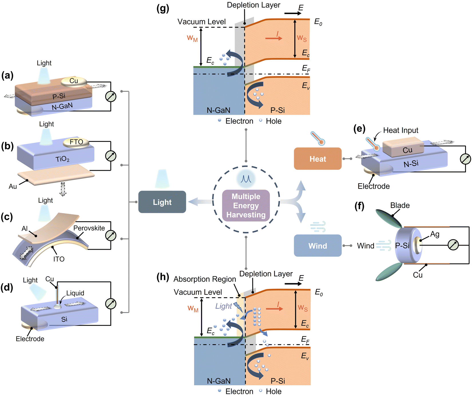 | ||
| Fig. 11 Coupling of different energies and the mechanisms. (a) Schematic diagram of the PN junction DC-TENG based on P–Si and N-GaN modulated with UV light. (b) Schematic diagram of the light-modulated M–S DC-TENG based on Au and TiO2. (c) Schematic diagram of the flexible light and mechanical energy co-harvesting TENG based on an Al/perovskite Schottky junction. (d) Schematic diagram of the optically coupled L–S contact device with a quartz tube dragging the water droplets on the surface of Si and TiO2. (e) Schematic diagram of the coupled tribo-thermoelectric and tribovoltaic effect based on the Cu–Si interface. (f) Schematic diagram of a wind-driven semiconductor TENG based on a dynamic Cu/P–Si Schottky junction. (g and h) Working mechanisms of the device before (g) and after (h) light irradiation. | ||
In addition, a metal–semiconductor DC-TENG based on Au/TiO2 is reported in which the current polarity can be rapidly reversed after illumination compared to the dark state (Fig. 11b). Its positive and negative ISCs increase 12 times and 2 times, respectively, and the photocurrent is saturated at 5 nA. The reversal of current polarity and the significant increase in current output can be attributed to the accumulation of a large number of photoelectrons on the surface of TiO2 and the increased conductivity under light illumination.83 Another flexible DC-TENG based on dynamic Al/perovskite Schottky junctions is demonstrated for the coupling of photonic/mechanical energy harvesting (Fig. 11c), which has a pulse voltage output of 0.70 V and a current density of 41.1 A m−2 (3 times higher than that in the dark environment). The device exhibits no obvious performance degradation under 120° bending and still maintains 70% of the original voltage output. This result indicates that the flexible Al/perovskite DC-TENG is promising as a flexible portable power source.81 The photonic energy harvesting can also be coupled with liquid–semiconductor devices as shown in Fig. 11d, where a quartz tube with an inner Cu electrode drags a water droplet to slide between the silicon and TiO2 surfaces. The photoexcited electron–hole pairs at the liquid–solid interface can increase the triboelectric current, which can be enhanced by increasing the light intensity or decreasing the light wavelength.84 The above studies indicate that the output performance of DC-TENGs can be readily improved by the coupled tribovoltaic and photovoltaic effects, which can synergistically advance the rapid development of hybridized photonic/mechanical energy harvesting.
7.2 Thermal energy
The coupling of tribo-thermoelectric and tribovoltaic effects is investigated in the DC-TENG based on the mechanical friction at the Cu–Si interface (Fig. 11e).58 The results show that the corresponding DC outputs consist of two parts: the stable part of thermoelectric current/voltage and the fluctuating part of triboelectric current/voltage. Tribo-excited electron–hole pairs are directionally separated to generate electric current under a built-in electric field. Meanwhile, the frictional heat drives the majority carriers to move along the temperature gradient. A higher sliding speed and load pressure can increase the tribovoltaic current, as well as the thermoelectric voltage and current, which is consistent with the influence of external factors, as discussed in Section 6. This study presents the multiphysics coupling effect by the combination of triboelectrification and semiconductor devices, exhibiting the possibility of semiconductor device based multisource energy harvesting.7.3 Wind energy
A wind-driven DC-TENG based on a dynamic Cu/P–Si Schottky junction (Fig. 11f) can output a continuous ultrahigh current with an average value of 4.4 mA and a maximum value of 8.4 mA for 740 seconds. Compared with previous metal–semiconductor DC-TENGs, the achieved current output is thousand times higher. Moreover, this TENG can reduce the cost compared with the current wind-power-generation strategies as it only consists of a simple contact structure (between a metal and a semiconductor) paired with a management circuit. The mechanism is that the dynamic construction and destruction of the built-in electric field can make the diffused charge carriers continuously bounce back and result in a continuous current output. Due to its stable output, this wind turbine has been used as a revolution counter and used to drive a graphene UV photodetector (photo responsivity of 35.8 A W−1). The DC-TENG coupled with wind energy provides an effective method to harvest wind power and directly power the distributed sensors in IoTs due to its ultrahigh DC output, small material wear, high durability and stability, simple structure, low cost, and good portability.85 Compared with conventional wind-energy-harvesting AC-TENGs that cannot directly drive electronic devices along with problems of low energy conversion efficiency, serious device wear and tear, short working life, and high cut-in wind speed,86–88 DC-TENGs can achieve high charge density, requiring no rectification and energy storage units.89–93In brief, the multiple energy harvesting strategy can effectively enhance the DC-TENG outputs and offers an efficient way to broaden the applications of energy harvesting based on semiconductor devices.
8. Applications
According to the literature reports, DC-TENGs based on the tribovoltaic effect can be applied in various fields, including powering electronics (Fig. 12a shows lighting the LEDs,18Fig. 12b shows constant powering of an electronic watch45), IoTs applications (Fig. 12c and d show the DC-TENG structures applicable in IoTs in the future17), self-powered sensing (Fig. 12e shows a high-output DC-TENG for temperature sensors,23Fig. 12f shows a DC-TENG for wind sensors), energy harvesting (Fig. 12g shows an encapsulated silicon–water–silicon DC-TENG,21Fig. 12h shows a flexible metal/perovskite DC-TENG81), and wearable devices (Fig. 12i shows a graphene wristband made of DC-TENG,22Fig. 12j indicates a flexible textile DC-TENG34). More specifically, DC-TENG powered electronics encompass but are not limited to wearable electronic watches, electronic calculators, temperature and humidity meters, and smart bracelets.18,34,45 For IoTs applications, the DC-TENG does not require a rectifier bridge to light up LEDs or light bulbs,8,16,17,22,24 which is promising in the direct powering and modulation of various smart sensors or electronics in future IoTs. For sensing applications, DC-TENG hybridized with wind energy or wind-driven semiconductor DC-TENGs can be used for graphene photodetectors and UV sensors.85,94–96 For energy harvesting, the harvested electrical energy by DC-TENGs can directly and continuously charge capacitors.8,44,46 Multisource energy harvesting not only includes photonic energy, thermal energy, wind energy, and mechanical energy, but also has the multiphysics coupling effect of combined energy forms.58,81,85 For wearable devices, the dynamic Schottky junction DC-TENGs based on an Al slider and a poly(3,4-ethylenedioxythiophene)-coated textile are demonstrated to be used for flexible wearable products.34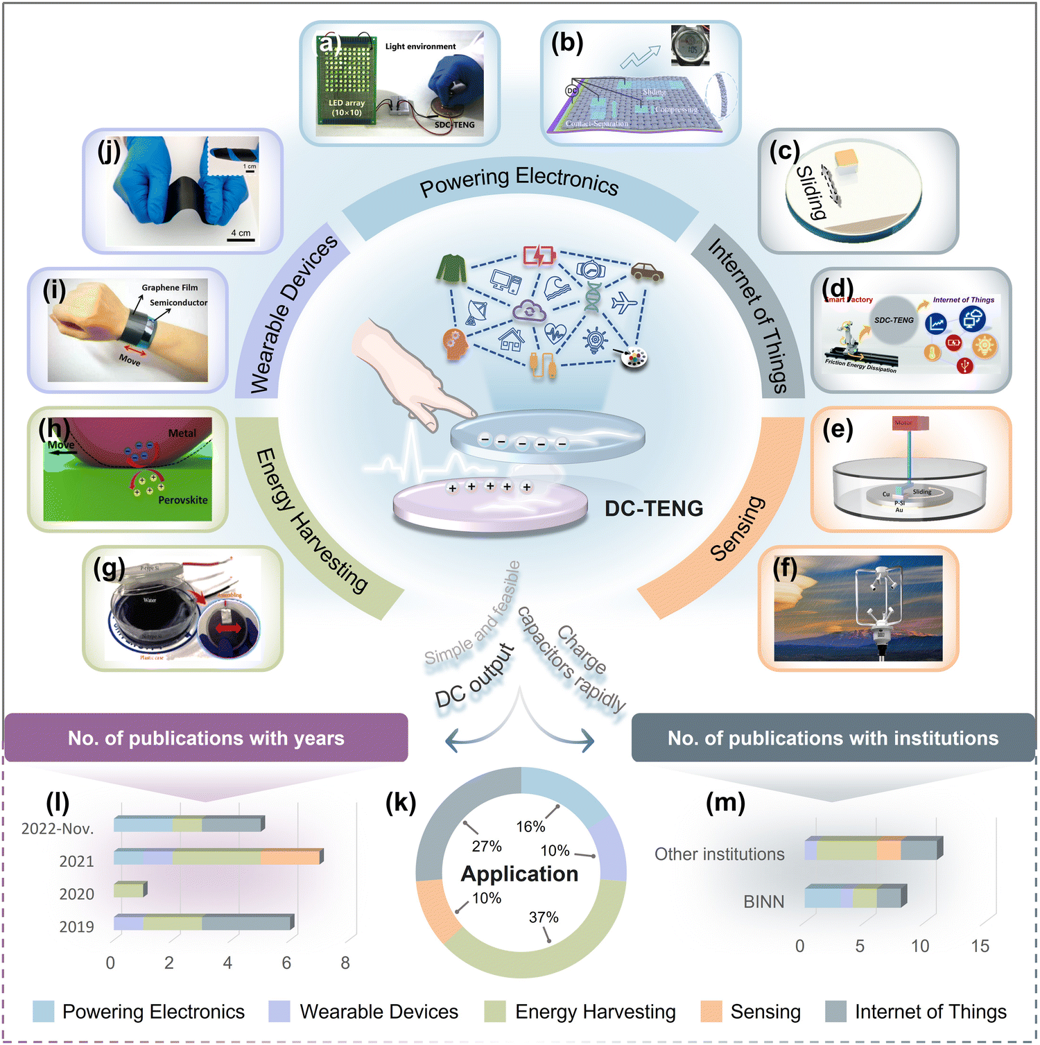 | ||
| Fig. 12 Applications of the DC-TENG in different fields and the current research situation of applications. (a–j) Applications of the DC-TENG in different fields. (a and b) Powering electronics. Reproduced with permission from ref. 18. Copyright 2022 Wiley-VCH GmbH. Modified with permission from ref. 45. Copyright 2022 The Royal Society of Chemistry. (c and d) The Internet of Things (IoTs). Modified with permission from ref. 17. Copyright 2022 The Royal Society of Chemistry. (e and f) Sensing. Reproduced with permission from ref. 23. Copyright 2021 Wiley-VCH GmbH. (g and h) Energy harvesting. Modified with permission from ref. 21. Copyright 2021 AAAS. Reproduced with permission from ref. 81. Copyright 2019 Elsevier Inc. (i and j) Wearable device. Reproduced with permission from ref. 22. Copyright 2018 Wiley-VCH Verlag GmbH & Co. KGaA, Weinheim. Reproduced with permission from ref. 34. Copyright 2021 American Chemical Society. (k) The percentage of reported applications in different fields. (l and m) The number of publications of DC-TENGs for different application fields in recent years (l) and by different institutions (m).8,16–18,21–24,34,44–46,58,81,85 | ||
TENGs possess unparalleled advantages in scavenging low-frequency and micromechanical energy.2,4,97 Conventional AC-TENGs have output instability89,98 and require additional rectification strategies (e.g., power management circuits,99–102 electric brushes,103,104 and rectifier bridges),105–110 which may reduce the portability and energy utilization efficiency and increase restrictions on powering electronic devices (or charging energy storage devices). In contrast, DC-TENGs have the advantage of efficient DC outputs and fast charging without the need for complex rectification circuits and energy storage units,43,44,111 providing a simple and feasible approach to converting low-frequency disordered mechanical energy (especially biomechanical energy, wind energy, and wave energy) into electrical energy. Current applications of DC-TENGs based on the tribovoltaic effect demonstrate huge potential in driving widely distributed sensors in IoTs,44 self-driven wearable devices, artificial intelligence, and industrial analog signal transmission.43 The statistical diagram of the reported applications in different fields is demonstrated in Fig. 12k. The statistical distributions of recently published research articles on DC-TENGs by different institutions are also shown in Fig. 12l and m.8,16–18,21–24,34,44–46,58,81,85 Although the number of articles is not particularly high, the literature investigation can indicate which application areas are currently relatively well researched and which are relatively blank. It can be used to guide related research in the future, which is important to promote multidisciplinary investigation on DC-TENGs. The above discussed practical applications based on DC-TENGs are expected to lead people's lifestyles toward more intelligent and self-powered directions in the near future.
9. Outlook
In recent years, the pursuit of DC-TENGs has made significant progress from the aspects of materials, structures, and device parameters, as well as coupling strategies with other energy sources. However, this technique still faces many challenges, which will be discussed below (Fig. 13).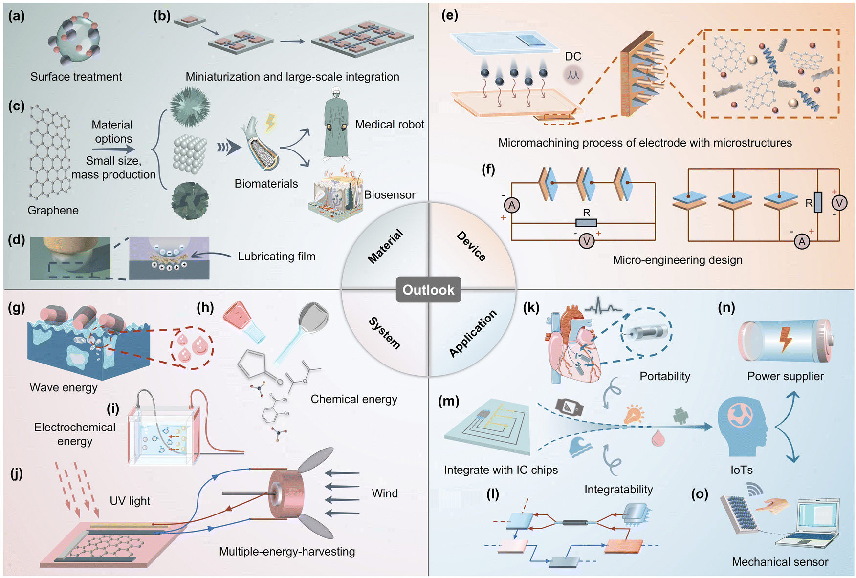 | ||
| Fig. 13 Outlook for DC-TENGs based on the tribovoltaic effect. (a) Schematic diagram of the surface treatment of the material. (b) Schematic diagram of high-performance device miniaturization and large-scale integration. (c) Schematic diagram of the exploitation of various nanomaterials, and even biomaterials that can be used for DC-TENGs in the biological applications. (d) Schematic diagram of lubricants between two materials. (e) Schematic diagram of the micromachining process of the electrode with microstructures. (f) Schematic diagram of microengineering design by an array of tips in series or in parallel. (g–i) Schematic diagram of wave energy (g), chemical energy (h) and electrochemical energy (i). (j) Schematic diagram of multiple-energy-harvesting (wind and photonic energy). (k and l) Schematic diagram taking portability (k) and integrability (l) into consideration in widespread applications of DC-TENGs. (m–o) Schematic diagram of devices integrated with other semiconductor devices and IC chips (m) as power suppliers (n) or mechanical sensors (o). | ||
Materials
The proposed tribovoltaic effect not only expands the material choices for TENGs from organic insulating polymers to semiconductors, but also demonstrates a novel electrical energy conversion mechanism of triboelectrification phenomena at the dynamic metal–semiconductor contact or PN junction. The tribovoltaic effect may also promote the deep coupling of triboelectric potential and semiconductor devices in the emerging field of tribotronics112,113 and triboiontronics.10,114,115 However, there are still several nonnegligible aspects in this field that require further investigation.First, regarding the output performance, surface treatment (or modification) of the material (Fig. 13a) can improve the surface state and increase the output current and current density of the DC-TENG. The mechanism is that electron–hole pairs at the interface may be excited by (i) the energy released during the electron transition from the surface state of one semiconductor to the surface state of the other semiconductor or (ii) the energy released during the formation of bonds at the sliding interface.19 Moreover, the charged surface state after surface treatment can effectively accelerate the charge carriers to pass through the large atomic electric field and can excite more electrons.43 It has been reported that N-type diamond coated tips sliding on silicon samples with different doping concentrations can generate different DC signals. The surface state density of the silicon sample is significantly improved by using ICP-RIE, and the results show that the triboelectric current of the device increases with increasing surface state density.19 However, due to equipment limitations and complex processes, it is crucial to find an economical and effective surface treatment or modification technique in the future.
Second, regarding the scale-up of energy harvesting and related applications, there are urgent requirements for high-performance device miniaturization and large-scale integration. It is also necessary to indicate that the DC-TENGs can be arrayed for large-scale integration and energy harvesting. Conventional rigid or dynamic DC-TENGs can also be extended to flexible counterparts for large-scale applications based on intensively developed flexible semiconductors and electrodes (Fig. 13b). Starting from the semiconductors that are commonly used nowadays (e.g., Si, graphene), seeking more advantageous semiconductors, such as more advanced 3D semiconductors or emerging 2D materials (or other nanomaterials),116–123 is expected to further shrink the device size, achieve mass production, and extend Moore's Law from the aspect of energy scavenging and energy utilization.9,11,89,111,124 Besides, the exploitation of biocompatible nanomaterials is especially important for biological applications of DC-TENGs, e.g., harvesting the vibration energy from human blood vessels and directly powering medical microrobots or biosensors (Fig. 13c).9
Finally, in terms of durability, the DC-TENGs developed so far have failed to simultaneously achieve high current density and long cycle life due to abrasion problems during frequent friction.9 Therefore, seeking wear-resistant semiconductor materials and developing lubricants (Fig. 13d) that can effectively reduce wear and exert lubricating effects are crucial for practical applications.45,73 The first microscale Schottky superlubric generator (S-SLG) with a high DC density and ultralong life was reported in 2021, which was made of microsized graphite flakes and N–Si. No wear or current decay was observed in the sliding contact process, promising the S-SLG with much longer lifetime. Accordingly, how to simultaneously achieve a sufficiently high current density and long product life cycle is a critical issue that needs to be further explored.9
Structures
When the electrodes of the DC-TENG are prepared with microstructures by a micromachining process (Fig. 13e), more efficient DC energy generation can be expected.5 Output characteristics can be further improved by microengineering design combined with multiple device connection, e.g., preparing a microtip array on the friction layer of DC-TENGs in series or in parallel (Fig. 13f).34,67,125 To scale up the energy harvesting capacity of DC-TENGs, in addition to potential gradient modification and material screening, it is also of great significance to optimize/modulate the device/electrode structures through micro/nanofabrication in future work.5,67,126 More attempts can also be made to develop a turntable device structure for DC-TENGs to further boost the output performance. Appropriate integration and encapsulation strategies can help to facilitate the energy harvesting efficiency and device durability for TENG in variable environments, e.g., for energy-harvesting at the solid–liquid interface between the rainwater and active solid materials during raining days.Multiple energy harvesting
Apart from the light, heat, and wind energies mentioned in this study, more energy forms (e.g., wave energy (Fig. 13g),127 chemical energy (Fig. 13h),128 electrochemical energy (Fig. 13i),129 photothermal energy130) can be adopted for energy coupling with the DC-TENG. In addition, the multiple forms of energy can be coupled together (or on demand) with mechanical energy to realize multiple-strategy energy-harvesting (or multifunctional) DC-TENGs based on a more sophisticated device design, e.g., the coupling of wind and photonic energy (Fig. 13j).85Applications
Semiconductor DC-TENGs with ultrahigh voltage and power density have great potential to be used to power various IoT-related sensors in the near future. Widespread applications of DC-TENGs should take portability (Fig. 13k) and integrability (Fig. 13l) into consideration.5 Since doped semiconductors can be used directly as electrodes, these devices can be easily integrated with other semiconductor devices and IC chips (Fig. 13m) as power suppliers (Fig. 13n) or mechanical sensors (Fig. 13o),67 which will also greatly contribute to carbon neutralization and carbon peaking.17 Furthermore, DC-TENGs provide a novel and promising method for harvesting energy from widely available water droplets in nature.21,4610. Conclusions
In summary, the development progress and microscopic mechanisms of DC-TENGs based on the tribovoltaic effect are elaborately summarized for the first time.First, DC-TENGs based on the tribovoltaic effect are systematically classified into six categories according to the materials and structures, namely, metal–semiconductor contact devices, metal–insulator–semiconductor contact devices, semiconductor–semiconductor contact devices, semiconductor–insulator–semiconductor contact devices, liquid–semiconductor contact devices, and metal/semiconductor–liquid–semiconductor contact devices. With an in-depth discussion of microscopic and macroscopic mechanisms, this review has comprehensively summarized and compared the output performances of different devices from the aspects of current density, peak power density, open-circuit voltage, short-circuit current, peak power output, and internal resistance.
Second, relevant strategies have been proposed to improve the output performance from three perspectives, namely, materials (different solid materials, insulator layers, and liquid materials) and structures (sliding structure,11 needle tip structure,43 rotating structure,8 interlayer structure,39 rolling structure,16 sphere-plane structure73), main external parameters (speed, load pressure, external resistance, etc.), and multiple energy harvesting strategies (photonic energy, thermal energy, and wind energy).
Third, suitable suggestions are provided on how to effectively boost the power output of the DC-TENG, including the utilization of active materials with a relatively larger Fermi level difference, a possible dielectric layer with increased barrier height, appropriate liquid choice, and optimal structure. By customizing the materials and structures of the DC-TENG, its current output, voltage output, and internal resistance can be effectively controlled to optimize the power output.10 For instance, higher frictional speed and load pressure can also increase the voltage output of the DC-TENG; higher frictional speed and load pressure combined with larger contact area can increase the current output of the DC-TENG; higher frictional speed and load pressure combined with smaller contact area can increase the peak power density of the DC-TENG.43,131
Finally, the review has explored the possible applications of DC-TENGs based on the tribovoltaic effect with consideration of potential challenges and development prospects in the future.
In recent years, the tribovoltaic effect widely occurring at various semiconductor material interfaces has been intensively investigated, and the output of the DC-TENG based on the tribovoltaic effect has been continuously optimized by different methods (e.g., surface modification and material/structure selection). Owing to the promising characteristics of high current density without a rectifier and continuous output performance, the DC-TENG has great potential for solving power supply problems in miniaturized electronic devices. It can also be directly used as an energy supply unit or self-powered sensor in sensor networks, IoTs, and smart factory applications. These achievements indicate that the tribovoltaic effect has huge potential in the future development of nano energy.131 This review may attract great research interests from scientists in the field of materials science, device engineering, electronic engineering, information technology, etc., which is of great importance to promote multidisciplinary investigation on DC-TENGs. It is expected that the diversified DC-TENGs will bring about revolutionary development in high-efficiency energy harvesting and broaden extensive applications in intelligent IoTs.
Author contributions
Q. S., C. X., and Z. L. W. conceived the idea. C. X. investigated the literature. C. X., J. Y., Z. H., Y. W., Q. S., and Z. L. W. discussed the working mechanism and review logic. C. X. prepared the figures and drafted the manuscript. C. X. and Q. S. revised the manuscript. Z. L. W. and Q. S. guided the whole project. All the authors discussed and commented on the manuscript.Conflicts of interest
There are no conflicts to declare.Acknowledgements
This work is supported by the National Key Research and Development Program of China (2021YFB3200304), the National Natural Science Foundation of China (52073031), Beijing Nova Program (Z191100001119047, Z211100002121148), Fundamental Research Funds for the Central Universities (E0EG6801X2), and the “Hundred Talents Program” of the Chinese Academy of Sciences.References
- W. Li and S. B. Gao, Energy, 2018, 165, 33–54 CrossRef.
- J. Zhao, G. Zhen, G. Liu, T. Bu, W. Liu, X. Fu, P. Zhang, C. Zhang and Z. L. Wang, Nano Energy, 2019, 61, 111–118 CrossRef CAS.
- J. Luo, Z. Wang, L. Xu, A. C. Wang, K. Han, T. Jiang, Q. Lai, Y. Bai, W. Tang, F. R. Fan and Z. L. Wang, Nat. Commun., 2019, 10, 5147 CrossRef PubMed.
- S. Niu and Z. L. Wang, Nano Energy, 2015, 14, 161–192 CrossRef CAS.
- J. Liu, A. Goswami, K. Jiang, F. Khan, S. Kim, R. McGee, Z. Li, Z. Hu, J. Lee and T. Thundat, Nat. Nanotechnol., 2018, 13, 112–116 CrossRef CAS PubMed.
- Z. L. Wang, ACS Nano, 2013, 7, 9533–9557 CrossRef CAS PubMed.
- Z. L. Wang and A. C. Wang, Mater. Today, 2019, 30, 34–51 CrossRef CAS.
- Y. Lu, Z. Hao, S. Feng, R. Shen, Y. Yan and S. Lin, iScience, 2019, 22, 58–69 CrossRef CAS PubMed.
- X. Huang, X. Xiang, J. Nie, D. Peng, F. Yang, Z. Wu, H. Jiang, Z. Xu and Q. Zheng, Nat. Commun., 2021, 12, 2268 CrossRef CAS PubMed.
- Z. Zhang, D. Jiang, J. Zhao, G. Liu, T. Bu, C. Zhang and Z. L. Wang, Adv. Energy Mater., 2020, 10, 1903713 CrossRef CAS.
- R. Xu, Q. Zhang, J. Y. Wang, D. Liu, J. Wang and Z. L. Wang, Nano Energy, 2019, 66, 104185 CrossRef CAS.
- J. Chen, G. Zhu, W. Yang, Q. Jing, P. Bai, Y. Yang, T. C. Hou and Z. L. Wang, Adv. Mater., 2013, 25, 6094–6099 CrossRef CAS PubMed.
- Y. Yang, H. Zhang and Z. L. Wang, Adv. Funct. Mater., 2014, 24, 3745–3750 CrossRef CAS.
- C. Xu, A. C. Wang, H. Zou, B. Zhang, C. Zhang, Y. Zi, L. Pan, P. Wang, P. Feng, Z. Lin and Z. L. Wang, Adv. Mater., 2018, 30, e1803968 CrossRef PubMed.
- L. Xu, T. Z. Bu, X. D. Yang, C. Zhang and Z. L. Wang, Nano Energy, 2018, 49, 625–633 CrossRef CAS.
- Y. Chen, Z. Zhang, Z. Wang, T. Bu, S. Dong, W. Wei, Z. Chen, Y. Lin, Y. Lv, H. Zhou, W. Sun and C. Zhang, ACS Appl. Mater. Interfaces, 2022, 14, 24020–24027 CrossRef CAS PubMed.
- Z. Z. Wang, Z. Zhang, Y. K. Chen, L. K. Gong, S. C. Dong, H. Zhou, Y. Lin, Y. Lv, G. X. Liu and C. Zhang, Energy Environ. Sci., 2022, 15, 2366–2373 RSC.
- Z. Zhang, Z. Wang, Y. Chen, Y. Feng, S. Dong, H. Zhou, Z. L. Wang and C. Zhang, Adv. Mater., 2022, 34, e2200146 CrossRef PubMed.
- M. Zheng, S. Lin, L. Xu, L. Zhu and Z. L. Wang, Adv. Mater., 2020, 32, e2000928 CrossRef PubMed.
- J. Liu, M. M. Miao, K. R. Jiang, F. Khan, A. Goswami, R. Mcgee, Z. Li, L. Nguyen, Z. Y. Hu, J. Lee, K. Cadien and T. Thundat, Nano Energy, 2018, 48, 320–326 CrossRef CAS.
- Y. Lu, Y. Yan, X. Yu, X. Zhou, S. Feng, C. Xu, H. Zheng, Z. Yang, L. Li, K. Liu and S. Lin, Research (Wash D C), 2021, 2021, 7505638 CAS.
- S. Lin, Y. Lu, S. Feng, Z. Hao and Y. Yan, Adv. Mater., 2019, 31, e1804398 Search PubMed.
- H. N. Zheng, R. J. Shen, H. K. Zhong, Y. H. Lu, X. T. Yu and S. S. Lin, Adv. Funct. Mater., 2021, 31, 2105325 CrossRef CAS.
- Y. Lu, S. Feng, R. Shen, Y. Xu, Z. Hao, Y. Yan, H. Zheng, X. Yu, Q. Gao, P. Zhang and S. Lin, Research (Wash D C), 2019, 2019, 5832382 CAS.
- Y. S. Zhou, S. Wang, Y. Yang, G. Zhu, S. Niu, Z. H. Lin, Y. Liu and Z. L. Wang, Nano Lett., 2014, 14, 1567–1572 CrossRef CAS PubMed.
- S. Lin, L. Xu, C. Xu, X. Chen, A. C. Wang, B. Zhang, P. Lin, Y. Yang, H. Zhao and Z. L. Wang, Adv. Mater., 2019, 31, e1808197 CrossRef PubMed.
- S. Lin, L. Xu, A. Chi Wang and Z. L. Wang, Nat. Commun., 2020, 11, 399 CrossRef CAS PubMed.
- Y. Song, N. Wang, Y. Wang, R. Zhang, H. Olin and Y. Yang, Adv. Energy Mater., 2020, 10, 2002756 CrossRef CAS.
- M. Alexe and D. Hesse, Nat. Commun., 2011, 2, 256 CrossRef.
- O. Hod, E. Meyer, Q. Zheng and M. Urbakh, Nature, 2018, 563, 485–492 CrossRef CAS PubMed.
- I.-G. Kim, K. J. Choi and J.-L. Lee, J. Vac. Sci. Technol., B: Microelectron. Nanometer Struct.--Process., Meas., Phenom., 2005, 23, 495 CrossRef CAS.
- W.-H. Lan, K.-C. Huang and K. F. Huang, Solid-State Electron., 2006, 50, 1677–1681 CrossRef CAS.
- J. Liu, K. Jiang, L. Nguyen, Z. Li and T. Thundat, Mater. Horiz., 2019, 6, 1020–1026 RSC.
- J. Meng, Z. H. Guo, C. X. Pan, L. Y. Wang, C. Y. Chang, L. W. Li, X. Pu and Z. L. Wang, ACS Energy Lett., 2021, 6, 2442–2450 CrossRef CAS.
- S. Q. Lin, X. Y. Chen and Z. L. Wang, Nano Energy, 2020, 76, 105070 CrossRef CAS.
- N. S. Lewis, J. Phys. Chem. B, 1998, 102, 4843–4855 CrossRef CAS.
- A. Iqbal, M. S. Hossain and K. H. Bevan, Phys. Chem. Chem. Phys., 2016, 18, 29466–29477 RSC.
- M. Zheng, S. Lin, L. Zhu, Z. Tang and Z. L. Wang, Adv. Mater. Interfaces, 2021, 9, 2101757 CrossRef.
- Y. Yan, X. Zhou, S. Feng, Y. Lu, J. Qian, P. Zhang, X. Yu, Y. Zheng, F. Wang, K. Liu and S. Lin, J. Phys. Chem. C, 2021, 125, 14180–14187 CrossRef CAS.
- Z. L. Wang, J. Chen and L. Lin, Energy Environ. Sci., 2015, 8, 2250–2282 RSC.
- Z. L. Wang, Mater. Today, 2017, 20, 74–82 CrossRef.
- X. Huang, L. Lin and Q. Zheng, Nano Energy, 2020, 70, 104494 CrossRef CAS.
- S. Lin, R. Shen, T. Yao, Y. Lu, S. Feng, Z. Hao, H. Zheng, Y. Yan and E. Li, Adv. Sci., 2019, 6, 1901925 CrossRef CAS PubMed.
- Y. Lu, Q. Gao, X. Yu, H. Zheng, R. Shen, Z. Hao, Y. Yan, P. Zhang, Y. Wen, G. Yang and S. Lin, Research (Wash D C), 2020, 2020, 5714754 CAS.
- J. Meng, C. Pan, L. Li, Z. H. Guo, F. Xu, L. Jia, Z. L. Wang and X. Pu, Energy Environ. Sci., 2022, 15, 5159–5167 RSC.
- Z. Wang, S. Dong, B. Fan, Y. Feng, Z. Zhang and C. Zhang, J Mater. Chem. A, 2022, 10, 25230–25237 RSC.
- U. Liu, M. I. Cheikh, R. M. Bao, H. H. Peng, F. F. Liu, Z. Li, K. R. Jiang, J. Chen and T. Thundat, Adv. Electron. Mater., 2019, 5, 1900464 CrossRef.
- H. Shao, J. Fang, H. X. Wang, H. T. Niu, H. Zhou, Y. Y. Cao, F. Y. Chen, S. D. Fu and T. Lin, Nano Energy, 2019, 62, 171–180 CrossRef CAS.
- R. Z. Yang, M. Benner, Z. P. Guo, C. Zhou and J. Liu, Adv. Funct. Mater., 2021, 31, 2103132 CrossRef CAS.
- H. Shao, J. Fang, H. Wang, L. Dai and T. Lin, Adv. Mater., 2016, 28, 1461–1466 CrossRef CAS PubMed.
- H. Shao, J. Fang, H. Wang, H. Zhou and T. Lin, J. Mater. Chem. A, 2017, 5, 8267–8273 RSC.
- Z. You, S. Wang, Z. Li, Y. Zou, T. Lu, F. Wang, B. Hu, X. Wang, L. Li, W. Fang and Y. Liu, Nano Energy, 2022, 91, 106667 CrossRef CAS.
- S. P. S. Arya and H. P. Singh, Thin Solid Films, 1982, 91, 363–374 CrossRef CAS.
- H. B. Michaelson, J. Appl. Phys., 1977, 48, 4729–4733 CrossRef CAS.
- H. B. Michaelson, IBM J. Res. Dev., 1978, 22, 72–80 CAS.
- S. Naghdi, G. Sanchez-Arriaga and K. Y. Rhee, J. Alloys Compd., 2019, 805, 1117–1134 CrossRef CAS.
- S. Sarkar, E. Bekyarova and R. C. Haddon, Acc. Chem. Res., 2012, 45, 673–682 CrossRef CAS PubMed.
- Z. Zhang, T. He, J. Zhao, G. Liu, Z. L. Wang and C. Zhang, Mater. Today Phys., 2021, 16, 100295 CrossRef CAS.
- S. Bastide, R. Butruille, D. Cahen, A. Dutta, J. Libman, A. Shanzer, L. Sun and A. Vilan, J. Phys. Chem. B, 1997, 101, 2678–2684 CrossRef CAS.
- C. P. Goyal, D. Goyal, S. K. Rajan, N. S. Ramgir, Y. Shimura, M. Navaneethan, Y. Hayakawa, C. Muthamizhchelvan, H. Ikeda and S. Ponnusamy, Crystals, 2020, 10, 188 CrossRef CAS.
- A. Imanishi, E. Tsuji and Y. Nakato, J. Phys. Chem. C, 2007, 111, 2128–2132 CrossRef CAS.
- R. Jacobs, J. Booske and D. Morgan, Adv. Funct. Mater., 2016, 26, 5471–5482 CrossRef CAS.
- N. Miura, T. Nanjo, M. Suita, T. Oishi, Y. Abe, T. Ozeki, H. Ishikawa, T. Egawa and T. Jimbo, Solid-State Electron., 2004, 48, 689–695 CrossRef CAS.
- B. Ryu, J. Korean Phys. Soc., 2018, 72, 122–128 CrossRef CAS.
- X. Y. Xue, C. L. Wang and W. L. Zhong, Surf. Sci., 2004, 550, 73–80 CrossRef CAS.
- S. M. Sze and K. K. Ng, Physics of Semiconductor Devices, John Wiley & Sons, New Jersey, 2007, pp. 79–196 Search PubMed.
- Q. Zhang, R. Xu and W. F. Cai, Nano Energy, 2018, 51, 698–703 CrossRef CAS.
- J. Shewchun, J. Dubow, A. Myszkowski and R. Singh, J. Appl. Phys., 1978, 49, 855–864 CrossRef CAS.
- X. Li, S. Lin, X. Lin, Z. Xu, P. Wang, S. Zhang, H. Zhong, W. Xu, Z. Wu and W. Fang, Opt. Express, 2016, 24, 134–145 CrossRef CAS PubMed.
- C. Liu, Z. Hu, Q. Wu, X. Wang, Y. Chen, W. Lin, H. Sang, S. Deng and N. Xu, Appl. Surf. Sci., 2005, 251, 220–224 CrossRef CAS.
- S. Lin, X. Li, P. Wang, Z. Xu, S. Zhang, H. Zhong, Z. Wu, W. Xu and H. Chen, Sci. Rep., 2015, 5, 15103 CrossRef CAS PubMed.
- S. Xu, R. M. Jacobs, H. M. Nguyen, S. Hao, M. Mahanthappa, C. Wolverton and D. Morgan, J. Mater. Chem. A, 2015, 3, 17248–17272 RSC.
- D. Yang, L. Zhang, N. Luo, Y. Liu, W. Sun, J. Peng, M. Feng, Y. Feng, H. Wang and D. Wang, Nano Energy, 2022, 99, 107370 CrossRef CAS.
- H. K. Zhong, Z. Q. Wu, X. Q. Li, W. L. Xu, S. Xu, S. J. Zhang, Z. J. Xu, H. S. Chen and S. S. Lin, Carbon, 2016, 105, 199–204 CrossRef CAS.
- T. Ding, K. Liu, J. Li, G. Xue, Q. Chen, L. Huang, B. Hu and J. Zhou, Adv. Funct. Mater., 2017, 27, 1700551 CrossRef.
- G. Xue, Y. Xu, T. Ding, J. Li, J. Yin, W. Fei, Y. Cao, J. Yu, L. Yuan, L. Gong, J. Chen, S. Deng, J. Zhou and W. Guo, Nat. Nanotechnol., 2017, 12, 317–321 CrossRef CAS PubMed.
- J. Liu, F. Liu, R. Bao, K. Jiang, F. Khan, Z. Li, H. Peng, J. Chen, A. Alodhayb and T. Thundat, ACS Appl. Mater. Interfaces, 2019, 11, 35404–35409 CrossRef CAS PubMed.
- S. Lin, X. Chen and Z. L. Wang, Nano Energy, 2020, 76, 105070 CrossRef CAS.
- L. Ren, A. Yu, W. Wang, D. Guo, M. Jia, P. Guo, Y. Zhang, Z. L. Wang and J. Zhai, Nano Lett., 2021, 21, 10099–10106 CrossRef CAS PubMed.
- M. Bockowski, M. Iwinska, M. Amilusik, M. Fijalkowski, B. Lucznik and T. Sochacki, Semicond. Sci. Technol., 2016, 31, 093002 CrossRef.
- Z. Z. Hao, T. M. Jiang, Y. H. Lu, S. R. Feng, R. J. Shen, T. Y. Yao, Y. F. Yan, Y. Yang, Y. F. Lu and S. S. Lin, Matter, 2019, 1, 639–649 CrossRef CAS.
- Y. Q. Bie, Z. M. Liao, H. Z. Zhang, G. R. Li, Y. Ye, Y. B. Zhou, J. Xu, Z. X. Qin, L. Dai and D. P. Yu, Adv. Mater., 2011, 23, 649–653 CrossRef CAS PubMed.
- J. J. Han, X. D. Yang, L. P. Liao, G. D. Zhou, G. Wang, C. Y. Xu, W. Hu, M. E. R. Debora and Q. L. Song, Nano Energy, 2019, 58, 331–337 CrossRef CAS.
- M. L. Zheng, S. Q. Lin, Z. Tang, Y. W. Feng and Z. L. Wang, Nano Energy, 2021, 83, 105810 CrossRef CAS.
- X. Yu, H. Zheng, Y. Lu, R. Shen, Y. Yan, Z. Hao, Y. Yang and S. Lin, RSC Adv., 2021, 11, 19106–19112 RSC.
- Y. Wang, E. Yang, T. Chen, J. Wang, Z. Hu, J. Mi, X. Pan and M. Xu, Nano Energy, 2020, 78, 105279 CrossRef CAS.
- Y. Zhang, Q. Zeng, Y. Wu, J. Wu, S. Yuan, D. Tan, C. Hu and X. Wang, Nanomicro Lett., 2020, 12, 175 CrossRef CAS PubMed.
- C. Zhang, Y. Liu, B. Zhang, O. Yang, W. Yuan, L. He, X. Wei, J. Wang and Z. L. Wang, ACS Energy Lett., 2021, 1490–1499, DOI:10.1021/acsenergylett.1c00368.
- D. Liu, X. Yin, H. Guo, L. Zhou, X. Li, C. Zhang, J. Wang and Z. L. Wang, Sci. Adv., 2019, 5, eaav6437 CrossRef CAS PubMed.
- S. Xu, H. Guo, S. L. Zhang, L. Jin, W. Ding, X. Wang and Z. L. Wang, Appl. Phys. Lett., 2020, 116, 263901 CrossRef CAS.
- C. Shan, W. Liu, Z. Wang, X. Pu, W. He, Q. Tang, S. Fu, G. Li, L. Long, H. Guo, J. Sun, A. Liu and C. Hu, Energy Environ. Sci., 2021, 14, 5395–5405 RSC.
- Z. Zhao, L. Zhou, S. Li, D. Liu, Y. Li, Y. Gao, Y. Liu, Y. Dai, J. Wang and Z. L. Wang, Nat. Commun., 2021, 12, 4686 CrossRef CAS PubMed.
- S. Fu, W. He, H. Wu, C. Shan, Y. Du, G. Li, P. Wang, H. Guo, J. Chen and C. Hu, Nanomicro Lett., 2022, 14, 155 CAS.
- S.-H. Yoon, S.-W. Lee, Y.-H. Lee and J.-S. Oh, Sensors, 2006, 6, 712–726 CrossRef.
- B. Borie, J. Wahrhusen, H. Grimm and M. Kläui, Appl. Phys. Lett., 2017, 111, 242402 CrossRef.
- M. Cavaliere, O. McVeigh, H. A. Jaeger, S. Hinds, K. O'Donoghue and P. Cantillon-Murphy, IEEE Sens. J., 2020, 20, 8623–8630 Search PubMed.
- H. Yang, Y. Pang, T. Bu, W. Liu, J. Luo, D. Jiang, C. Zhang and Z. L. Wang, Nat. Commun., 2019, 10, 2309 CrossRef PubMed.
- H. Ryu, J. H. Lee, U. Khan, S. S. Kwak, R. Hinchet and S.-W. Kim, Energy Environ. Sci., 2018, 11, 2057–2063 RSC.
- S. Wang, X. Mu, Y. Yang, C. Sun, A. Y. Gu and Z. L. Wang, Adv. Mater., 2015, 27, 240–248 CrossRef CAS PubMed.
- K. Zhao, Z. L. Wang and Y. Yang, ACS Nano, 2016, 10, 9044–9052 CrossRef CAS PubMed.
- X. Wang and Y. Yang, Nano Energy, 2017, 32, 36–41 CrossRef CAS.
- X. Liang, T. Jiang, G. Liu, T. Xiao, L. Xu, W. Li, F. Xi, C. Zhang and Z. L. Wang, Adv. Funct. Mater., 2019, 29, 1807241 CrossRef CAS.
- C. Zhang, T. Zhou, W. Tang, C. Han, L. Zhang and Z. L. Wang, Adv. Energy Mater., 2014, 4, 1301798 CrossRef.
- J. Wang, Z. Wu, L. Pan, R. Gao, B. Zhang, L. Yang, H. Guo, R. Liao and Z. L. Wang, ACS Nano, 2019, 13, 2587–2598 CAS.
- J. Zhong, Q. Zhong, F. Fan, Y. Zhang, S. Wang, B. Hu, Z. L. Wang and J. Zhou, Nano Energy, 2013, 2, 491–497 CrossRef CAS.
- K. Zhang, X. Wang, Y. Yang and Z. L. Wang, ACS Nano, 2015, 9, 3521–3529 CrossRef CAS PubMed.
- S. Wang, X. Wang, Z. L. Wang and Y. Yang, ACS Nano, 2016, 10, 5696–5700 CrossRef CAS PubMed.
- S. Wang, Z. L. Wang and Y. Yang, Adv. Mater., 2016, 28, 2881–2887 CrossRef CAS PubMed.
- Q. Zhang, Q. Liang, Q. Liao, M. Ma, F. Gao, X. Zhao, Y. Song, L. Song, X. Xun and Y. Zhang, Adv. Funct. Mater., 2018, 28, 1803117 CrossRef.
- G.-Z. Li, G.-G. Wang, Y.-W. Cai, N. Sun, F. Li, H.-L. Zhou, H.-X. Zhao, X.-N. Zhang, J.-C. Han and Y. Yang, Nano Energy, 2020, 75, 104918 CrossRef CAS.
- Z. Zhao, Y. Dai, D. Liu, L. Zhou, S. Li, Z. L. Wang and J. Wang, Nat. Commun., 2020, 11, 6186 CrossRef CAS PubMed.
- G. Gao, B. Wan, X. Liu, Q. Sun, X. Yang, L. Wang, C. Pan and Z. L. Wang, Adv. Mater., 2018, 30, e1705088 CrossRef PubMed.
- J. Yu, X. Yang, G. Gao, Y. Xiong, Y. Wang, J. Han, Y. Chen, H. Zhang, Q. Sun and Z. L. Wang, Sci. Adv., 2021, 7, eabd9117 CrossRef CAS PubMed.
- G. Gao, J. Yu, X. Yang, Y. Pang, J. Zhao, C. Pan, Q. Sun and Z. L. Wang, Adv. Mater., 2019, 31, e1806905 CrossRef PubMed.
- J. Yu, G. Gao, J. Huang, X. Yang, J. Han, H. Zhang, Y. Chen, C. Zhao, Q. Sun and Z. L. Wang, Nat. Commun., 2021, 12, 1581 CrossRef CAS PubMed.
- S. Das, J. A. Robinson, M. Dubey, H. Terrones and M. Terrones, Annu. Rev. Mater. Res., 2015, 45, 1–27 CrossRef CAS.
- M. C. Lemme, D. Akinwande, C. Huyghebaert and C. Stampfer, Nat. Commun., 2022, 13, 1392 CrossRef CAS PubMed.
- G. Fiori, F. Bonaccorso, G. Iannaccone, T. Palacios, D. Neumaier, A. Seabaugh, S. K. Banerjee and L. Colombo, Nat. Nanotechnol., 2014, 9, 768–779 CrossRef CAS PubMed.
- Q. H. Wang, K. Kalantar-Zadeh, A. Kis, J. N. Coleman and M. S. Strano, Nat. Nanotechnol., 2012, 7, 699–712 CrossRef CAS PubMed.
- D. Akinwande, C. Huyghebaert, C. H. Wang, M. I. Serna, S. Goossens, L. J. Li, H. P. Wong and F. H. L. Koppens, Nature, 2019, 573, 507–518 CrossRef CAS PubMed.
- S. H. Choi, S. J. Yun, Y. S. Won, C. S. Oh, S. M. Kim, K. K. Kim and Y. H. Lee, Nat. Commun., 2022, 13, 1484 CrossRef CAS PubMed.
- M. A. M. Hasan, Y. Wang, C. R. Bowen and Y. Yang, Nanomicro Lett., 2021, 13, 82 Search PubMed.
- J. Yao, H. Wang, B. Yuan, Z. Hu, C. Wu and A. Zhao, Adv. Mater., 2022, e2200236, DOI:10.1002/adma.202200236.
- P. C. Shen, C. Su, Y. Lin, A. S. Chou, C. C. Cheng, J. H. Park, M. H. Chiu, A. Y. Lu, H. L. Tang, M. M. Tavakoli, G. Pitner, X. Ji, Z. Cai, N. Mao, J. Wang, V. Tung, J. Li, J. Bokor, A. Zettl, C. I. Wu, T. Palacios, L. J. Li and J. Kong, Nature, 2021, 593, 211–217 CrossRef CAS PubMed.
- C.-H. Sun, N. C. Linn and P. Jiang, Chem. Mater., 2007, 19, 4551–4556 CrossRef CAS.
- G. Zhu, Z. H. Lin, Q. Jing, P. Bai, C. Pan, Y. Yang, Y. Zhou and Z. L. Wang, Nano Lett., 2013, 13, 847–853 CrossRef CAS PubMed.
- Y. Xu, W. Yang, X. Lu, Y. Yang, J. Li, J. Wen, T. Cheng and Z. L. Wang, ACS Nano, 2021, 15, 16368–16375 CrossRef CAS PubMed.
- C. Huang, G. Lu, N. Qin, Z. Shao, D. Zhang, C. Soutis, Y. Y. Zhang, L. Mi and H. Hou, ACS Appl. Mater. Interfaces, 2022, 14, 16424–16434 CrossRef CAS PubMed.
- Z. Duan, Z. Yuan, Y. Jiang, Q. Zhao, Q. Huang, Y. Zhang, B. Liu and H. Tai, Chem. Eng. J., 2022, 446, 136910 CrossRef CAS.
- L. Li, S. Feng, Y. Bai, X. Yang, M. Liu, M. Hao, S. Wang, Y. Wu, F. Sun, Z. Liu and T. Zhang, Nat. Commun., 2022, 13, 1043 CrossRef CAS PubMed.
- S. Lin and Z. Lin Wang, Mater. Today, 2022 DOI:10.1016/j.mattod.2022.11.005.
| This journal is © The Royal Society of Chemistry 2023 |