DOI:
10.1039/C7MH00091J
(Communication)
Mater. Horiz., 2017,
4, 608-618
A unified understanding of charge transport in organic semiconductors: the importance of attenuated delocalization for the carriers†
Received
16th February 2017
, Accepted 27th March 2017
First published on 27th March 2017
Abstract
The variety of charge transport theories for organic semiconductors (OSCs) raises the question of which models should be selected for each case, and there is a lack of generalized understanding regarding various OSCs over the full range of crystallinity from single crystal to amorphous. Here, we report that the generalized Einstein relation (GER) can unify various theoretical models and predict charge transport in OSCs with various crystallinities, by altering the variance of the density of states and the delocalization degree in a Gaussian-distributed density of states. The GER also provides a good fitting to much of the experimental data of temperature- and gate-voltage-dependent mobility for different OSCs in transistors. Consequently, disorders of charge transport in various OSCs can be directly compared in the same map, which reveals how energetic disorder and the delocalization degree determine charge transport in organic devices.
Conceptual insights
Different classes of organic semiconductors (OSCs) have been described by various charge transport mechanisms from a model of band transport to variable range hopping, according to the molecular structure and crystallization. There is a lack of consensus in describing, predicting, and comparing transport in OSCs. This work describes a new understanding in charge transport, the generalized Einstein relation (GER), which unifies several classic theories for transport dynamics. By defining the variance in the density of states and delocalization degree, the GER predicts well the experimental data of a broad range of OSCs with various crystallinities, including temperature- and gate-voltage-dependent mobility data in transistors. The results are sufficiently general to allow a direct comparison of disorder factors in charge transport and provide guidelines to understand how energetic disorder and localization determine the electric characteristics of organic devices.
|
1. Introduction
Recently, many new organic semiconductors (OSCs) have been reported to exhibit high field-effect mobility (>10 cm2 V−1 s−1),1 despite the morphology of some thin films not being highly crystalline.2 For example, it is difficult to predict the charge transport properties through checking the crystallinity of state-of-the-art donor–acceptor (D–A) conjugated polymers by X-ray-based structural analysis tools as many of them exhibit a low crystallization degree or possess a non-crystalline nature.3 New types of methods need to be developed to further understand the charge transport of these new OSCs, and a general consensus is still far from being reached, especially for those OSCs with high structural disorder but with superb mobility.4 Unlike single-crystals, the abundant structural defects and strong lattice vibrations owing to the weak van der Waals interactions are inherent in OSCs and result in complicated transport mechanisms,5 which lead to the dependence of the mobility on the temperature and/or the carrier concentration.6
Up to now, different theories concerning microscopic charge transport mechanisms have been proposed and many of them have been supported by evidence in different experiments on the temperature dependence of carrier mobility with various materials.4a, 5a, 6b A brief summary of charge transport theories is given in Fig. 1, in which the theories are roughly classified according to the crystallinity or the structural disorder of the semiconductors: (1) classic band-like transport is expected for disorder-free OSCs, which are mainly single crystalline materials7 or some conjugated polymers with extremely low torsions of chains.8 (2) For polycrystalline OSCs with a low extent of structural disorder, the mobility edge model is applicable and it is similar to the multiple trap and release (MTR) model.6b,9 (3) In amorphous or highly disordered semiconductors, charge transport mainly occurs by hopping or tunneling among localized states, and the most commonly used models are the variable range hopping model,10 Bässler's Gaussian disorder model,6b,11 and the percolation model.6b,9a,12 Some of them are also considered for OSCs in a polycrystalline state. (4) As in many OSCs carrier transport along the polymeric backbone would require a reorganization energy and also the polarization effect exists, thus the Marcus charge transfer (CT) model13 should be considered. Furthermore, as the CT is driven by the coupling to nuclear vibrations (i.e. a heat bath),14 the effect of the local nuclear configurations should be taken into account, especially for non-polar OSCs where the relevant stretching vibrations are at a high frequency. This mechanism is described by the quantum nuclear tunneling (NT) theory,14,15 in which the carriers tunnel through the potential formed by the coupling of the electronic charge to its nuclear environment. Compared to the CT theory, the NT theory predicts higher values of mobility in the OSCs that are consistent with some experimental results.16
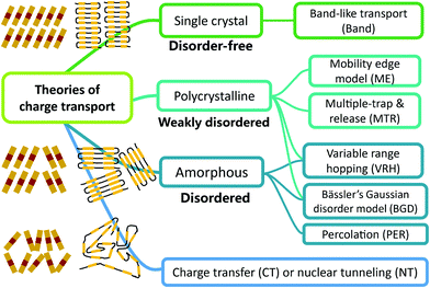 |
| | Fig. 1 A brief summary of charge transport theories in organic semiconductors. According to the degree of order or crystal structure of the semiconductor, these theories can be roughly divided into several categories. | |
Because of the large variance of the adapted models and their limitations in specific materials, the disorders of charge transport in different microscopic mechanisms and in different polymers cannot be directly and generally compared. In addition, as mentioned above, recent studies on the high mobility of non-crystalline OSCs imply that a more general description of charge transport disorder is needed. In this report, we present a generalized charge transport model that is valid for various OSCs with different morphologies by using the so-called generalized Einstein relation (GER). By altering the variance of the density of states (ΔE) and delocalization degree (ΔD) in a Gaussian-distributed density of states, the GER can describe well most charge carrier mobility dependencies on temperature as predicted by the aforementioned theories. This is also evidenced in experiments with various OSCs from single crystal small molecules to amorphous conjugated polymers, as well as the experimentally observed dependence of mobility on the charge carrier concentration. Consequently, the charge transport in various OSCs can be regarded as being determined by ΔE and ΔD, and the disorder in the charge transport can now be directly compared in the same map formed by the coordinates ΔE and ΔD.
2. Results and discussion
Description of charge transport
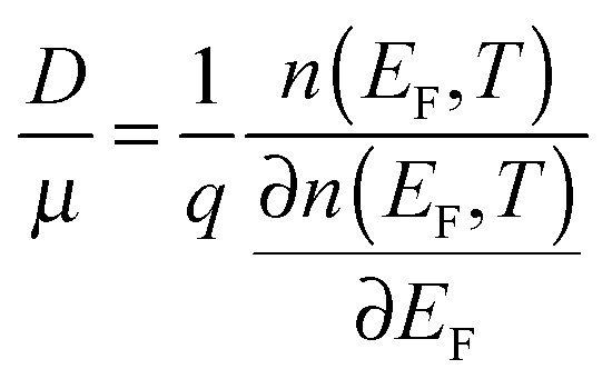
For a disorder-free, single crystalline semiconductor in the nondegenerate state (i.e., using the Boltzmann approximation), the Einstein relation between the diffusion coefficient D and the mobility μ takes its classical form: D/μ = kT/q, where k is Boltzmann's constant, T is the temperature, and q is the electron charge. In disordered semiconductors in the degenerate state, the ratio of the diffusion coefficient to the mobility becomes a function of the carrier concentration in the GER:17| | 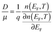 | (1) |
where n is the total carrier concentration and EF is the Fermi energy. In OSCs, eqn (1) should be used under the assumption that the mobility can also be a function of energy E, for example by assuming a certain hopping probability.18 We propose that the mobility can be calculated by using the GER, which is derived according to the special features of OSCs described below.
The first important feature of OSCs is the relatively weak bonding strength and electronic interactions between neighboring molecules, which result in the density of states (DOS) having a narrow Gaussian distribution:17,19
| | 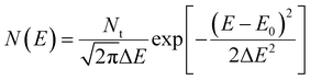 | (2) |
Here
Nt is the characteristic band DOS (usually 10
21 cm
−3), Δ
E is the variance of the Gaussian distributed DOS (usually below 0.2 eV), and
E0 is the energy of the DOS center (
E0 is referenced as 0 eV). The DOS with different Δ
E is illustrated in the ESI,
† Fig. S1. The second feature of OSCs is that in transistor operation the quasi Fermi level may not always be far from the edge of the conduction bands or levels (
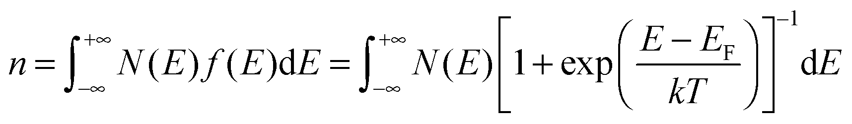
i.e. HOMO or LUMO levels), especially when the energy levels are strongly bent by gate-voltage tuning. Thus, degeneration has to be considered and so the Fermi–Dirac distribution is used to calculate the overall carrier density
n:
| | 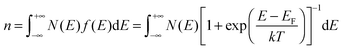 | (3) |
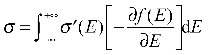
The third feature of OSCs is that defects or traps are abundant, and so electronic states in tails are more localized compared to those well above the tail states (as shown in
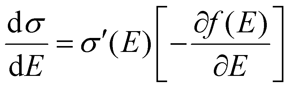
Fig. 2b). That being said, the microscopic conductivity of electronic states,
σ′, is energy-dependent rather than being constant:
10d,19bwhere
D(
E) is the diffusivity for each energy and will be discussed below. Thus, the overall conductivity
σ for all the carriers can be calculated by the Kubo–Greenwood integral:
10d,19b| |  | (5) |
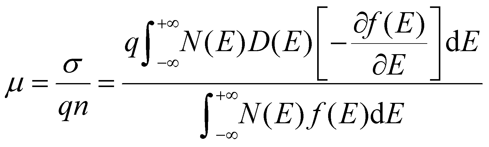
The above three features of OSCs in FETs,
i.e. weak bonding, degeneration, and defect-abundance, are quantified by
eqn (2)–(5), respectively, and we can use them to calculate the overall mobility for general OSCs by:
| | 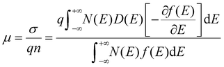 | (6) |
Eqn (6) quantifies the relationship between mobility and diffusivity, and thus provides a GER for disordered materials and especially for OSCs.
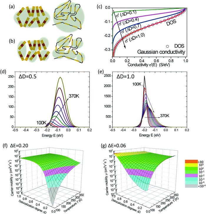 |
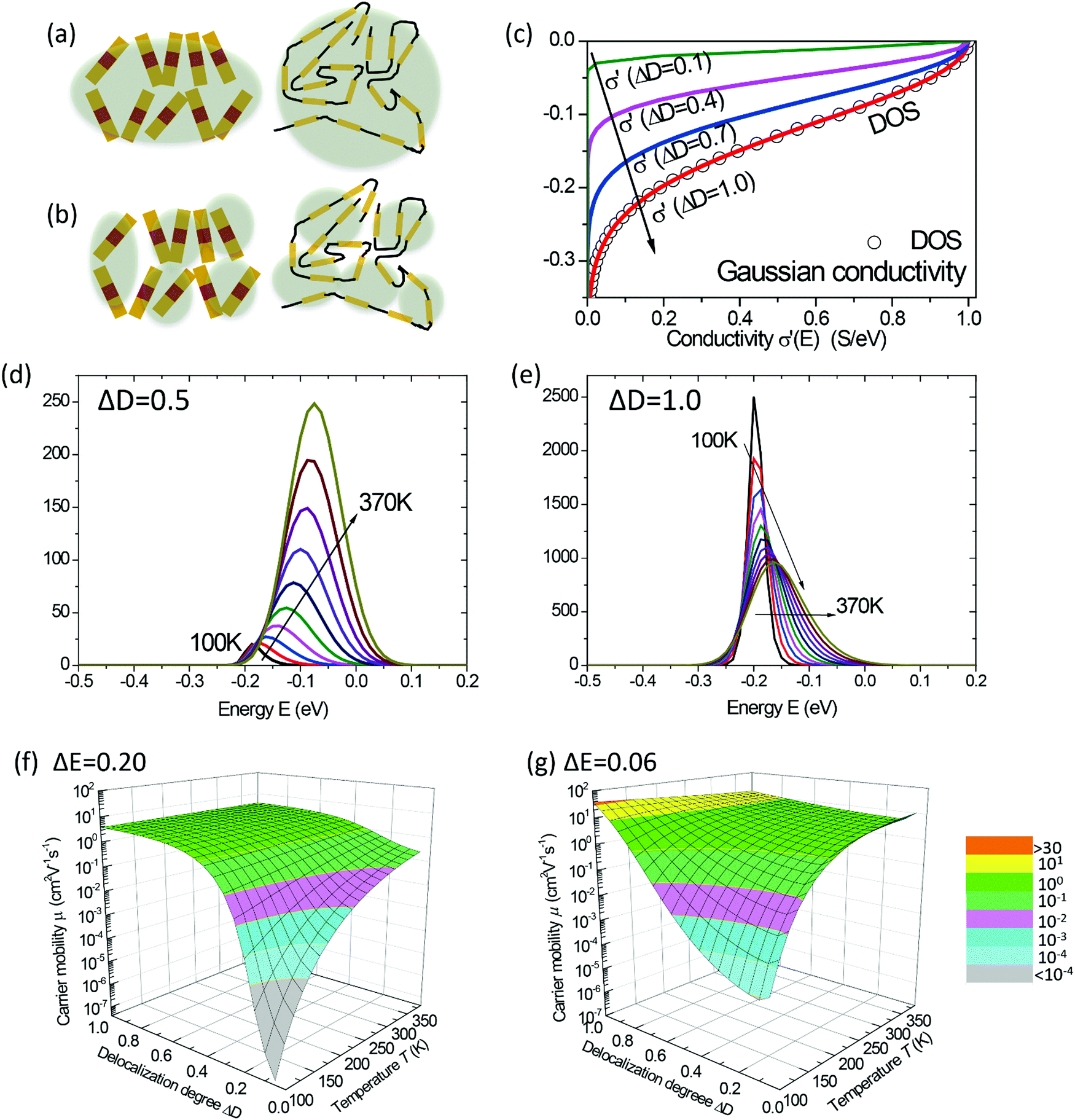
| | Fig. 2 (a and b) Schematic representations of the delocalization of carriers in the states with high energies near the DOS center (a) or in the states with low energies near the edge of the DOS (or near the energy gap) (b). The shades are illustrative of the delocalization area. (c) Normalized microscopic conductivity σ′(E) as a function of energy for different degrees of delocalization ΔD (ΔE is fixed at 0.11 eV). (d) and (e) The differential conductivities  for different temperatures with low or high delocalization degrees (ΔD = 0.5 or ΔD = 1). The temperatures are varied from T = 100 K up to 370 K (ΔE = 0.1 eV, EF = −0.2 eV). (f) and (g) The effective mobility as a function of temperature for various ΔD (ΔE = 0.20 and 0.06 eV, respectively; EF is fixed at −0.2 eV). The effective mobility decreases as the temperature increases at ΔD = 1, which is consistent with band-like transport. for different temperatures with low or high delocalization degrees (ΔD = 0.5 or ΔD = 1). The temperatures are varied from T = 100 K up to 370 K (ΔE = 0.1 eV, EF = −0.2 eV). (f) and (g) The effective mobility as a function of temperature for various ΔD (ΔE = 0.20 and 0.06 eV, respectively; EF is fixed at −0.2 eV). The effective mobility decreases as the temperature increases at ΔD = 1, which is consistent with band-like transport. | |
The diffusivity for each energy D(E) in eqn (4) should be defined considering the microscopic mechanisms of charge transport in OSC solids. On one hand, in perfect crystals the electronic orbits and the delocalization of charges within a molecule or among any adjacent molecules are identical throughout the solids, respectively, and together lead to the intrinsic transport properties of the electronic states in the whole DOS (Fig. 2a). In this case, the macroscopic charge transport properties would ideally follow the first-principles evaluations.16a,20 On the other hand, as microscopic voids, grain boundaries, polymeric twisting, or chemical impurities are often the origin of a large amount of tail states in the DOS, these states near the energy gap may exhibit transport properties seriously deviating from the intrinsic transport characteristics of the states near the center of the DOS, and they may possess a reduced delocalization length (or diffusion length) as compared to that predicted by the first-principles evaluations in the microscopic results (Fig. 2b). To this end, the attenuation of conductivity from the DOS center to the edge should be considered and, for generality, the diffusivity is assumed to be Gaussian-like19a and then σ′(E) can be described by:
| |  | (7) |
where
σ0 =
NCqμ0/2 is the characteristic conductivity and
μ0 is the characteristic mobility, which are material-specific. The characteristic parameter Δ
D (≤1, no unit) reflects the degree of delocalization for the electronic states near the edge of the DOS (near HOMO or LUMO levels): a small Δ
D means a severely attenuated
σ′(
E) from the center of the DOS (extended states) to the edge (localized states), and thus the tail states possess a much lower microscopic conductivity (
i.e. severely localized) than those near the center states. When Δ
D = 1, the delocalization degree is the same for the whole DOS and the shape of
σ′(
E) is only determined by the DOS (
Fig. 2c). For a reference, in the mobility edge (ME) model the states are divided into the delocalized states (
μ =
μ0) when
E ≥ ME and the totally localized tail states (
μ = 0) when
E < ME (ME denotes the energy as the mobility edge, see Fig. S2, ESI
†). Thus, above the ME, the diffusivity is constant and the microscopic conductivity is only determined by the DOS.
The above discussions do not rely on specific transport mechanisms and should apply to carrier transport in typical OSCs. It is worth noting that ΔE characterizes the degree of disorder in the energy structure and ΔD characterizes the degree of delocalization. Specifically, ΔE of the DOS is determined by the static or structural factors, including the crystallinity of the structure and the electronic interactions/coupling among neighboring molecules, while ΔD can be affected by similar factors as well as dynamic or external factors, such as lattice vibrations, scattering mechanisms, and properties of defects or traps. By only varying one parameter at a time, the differential conductivity  is plotted against energy E in Fig. 2d and e. When the temperatures are varied from T = 100 K up to 370 K, the maximum of
  increases homogeneously as the temperature increases in the case when ΔD = 0.5, and so does the overall conductivity (Fig. 2d). In comparison, in the case when ΔD = 1, the maximum of
  decreases as the temperature increases and the change in the overall conductivity becomes much smaller (Fig. 2e). The relationship between the mobility μ and the temperature T (μ–T relation) is then calculated in Fig. 2f and g, where the mobility at a certain temperature with varying ΔD or vice versa can be directly read. At a certain temperature, a larger DOS variance ΔE or a smaller delocalization degree ΔD results in a decreased mobility, which is highly consistent with the above physical understanding. As the temperature decreases, the mobility degrades sharply (or raises slightly) with a low (or high) delocalization degree, which is consistent with the transport mechanism being highly limited by thermal activation (or by lattice/phonon scattering). Importantly, the GER can explain the transition from the band-like temperature dependence of the mobility (i.e., dμ/dT < 0) to the thermally activated temperature dependence (i.e., dμ/dT > 0), which has been reported in some high mobility semiconductors in previous experiments21 and will be discussed below.
Various transport models
The relationship between the GER and the various charge transport mechanisms are studied in Fig. 3. According to the predictions from these theories, the μ–T relations are calculated for different transport models (symbols). For crystalline semiconductors, the mechanisms include band-like transport for single crystals (Fig. 3a and b) and for poly-crystals the multiple trapping and release (MTR) model, which takes a similar form to the mobility edge (ME) model (Fig. 3c and d). For amorphous semiconductors, the variable range hopping (VRH) model (Fig. 3e and f), Bässler's Gaussian disorder (BGD) model (Fig. 3g and h), and the percolation (PER) model (Fig. S3, ESI†) are mainly involved. The Marcus charge transfer (CT) model (Fig. 3i and j) and nuclear tunneling (NT) models (Fig. 3k and l) describe the reorganization effects in OSCs due to the coupling between charges and the local environment. These models have different views of microscopic dynamic processes and the factors in charge transport, and they have been applied to various semiconductors.6b,9–15 In each model, the key factors determining the μ–T relation are varied while keeping other parameters constant and these factors are provided along with the model (Fig. 3b, d, f, h, j and l). For instance, in the MTR model the mean energy of the trap states ET is varied to generate a series of data, and in the NT model αK (the Kondo parameter) is varied to describe the different coupling strengths between the charges and the aforementioned heat bath (i.e. nuclear vibrations).15a The ranges of these parameters were chosen essentially according to the values reported in previous literature. The μ–1/T relations described by the above mechanisms are fitted to the GER by varying ΔE and ΔD (lines). The fitting parameters are listed in Table S1 (ESI†) and the μ–T relations are also presented for a reference (Fig. S4, ESI†). In general, the fittings by the GER are reasonable over a large temperature range and deviations only occur at very low temperatures. Hence, the GER generally covers various transport behaviors and provides comparisons for charge transport in different mechanisms or materials.
 |
| | Fig. 3 Schematic representation of transport mechanisms for (a) band-like transport, (c) the multiple trap and release (MTR) model, (e) the variable range hopping (VRH) model (sketched in ref. 22), (g) Bässler's Gaussian disorder (BGD) model (sketched in ref. 11c), (i) the Marcus charge transfer (CT) model (plotted in ref. 13d), and (k) the nuclear tunneling model (NT), sketched in ref. 14 and 15 and the percolation (PER) model is given in Fig. S3 (ESI†) (PER, sketched in ref. 12). The temperature dependence of the mobility calculated by different transport models is plotted with symbols and the fitting by the GER is plotted with lines: (b) band model with varying scattering factor a. (d) The MTR model with varying mean energy of the trap states ET. (f) The VRH model with varying T1, proportional to the size of localized states. (h) The BGD model with varying width of the Gaussian function σ. (j) The CT model with varying reorganization energy λ. (l) The NT model with varying the Kondo parameter αK. (m) The values of delocalization degree ΔD and DOS variance ΔE parameters are plotted for all of the models with the corresponding key parameters. | |
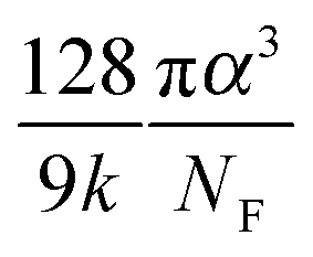
The values of the DOS variances ΔE and the delocalization degree ΔD are plotted for various transport mechanisms together with the corresponding key parameters in Fig. 3m. For example, in the VRH model T1 is defined as  , where α is the size of the localized state and NF is the density of states at the Fermi edge. In all of the cases, ΔE increases and ΔD decreases as those limiting factors increase, which is consistent with the physical mechanisms of these models. The DOS variance ΔE can be taken as a signature of energetic disorder, as it generally follows the energy disorder parameters in the different models, for example, T1 in the VRH model is proportional to the Urbach energy.23 By gathering all of the fitting values together in Fig. 3m, the impacts of different limiting factors in the various mechanisms of charge transport can now be quantitatively compared under the same axes constructed by ΔE and ΔD. Note that the CT model describes charge transport as being relatively concentrated in a low-disorder and high-delocalization area, while Bässler's Gaussian disorder (BGD) model covers the range in relatively lower degrees of delocalization. This is probably because the CT model mainly describes charge transport for polycrystalline polymers with a long conjugation length and short localized segments, while BGD is proposed for amorphous semiconductors where hopping among localized states is the main process.
Experimentally measured mobility
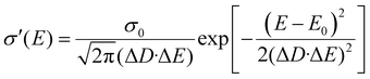
The GER was used to investigate the experimental data of μ–T measured for organic field-effect transistors (OFETs) made with different types of OSCs (Fig. 4). The studied materials included various OSCs from crystalline to amorphous: rubrene (Fig. 4a);7a pentacene (Fig. 4b)24; 6,13-bistriisopropylsilylethynyl pentacene (TIPS-PEN,25Fig. 4c); N-alkyl perylene diimides (PTCDI, Fig. 4d);26 a DPP-containing copolymer with siloxane-terminated butyl or pentyl chains (PTDPPSe-SiC4 and PTDPPSe-SiC5, Fig. 4e);27 cyclopentadithiophene-benzothiadiazole (CDT-BTZ-C12, Fig. 4f);28 poly(3-hexylthiophene) (P3HT, Fig. 4g);29 poly(2,5-bis(3-alkylthiophen-2-yl)thieno(3,2-b)thiophene) (PBTTT, Fig. 4h);30 [N,N′-bis(2-octyldodecyl)-1,4,5,8-naphthalenedicarboximide-2,6-diyl]-alt-5,5′-(2,2′-bithiophene) P(NDI2OD-T2) (Fig. 4i);31 and a D–A polymer containing diketopyrrolopyrrole (DPP), benzothiadiazole (BT), and selenophene (Se) (PSeDPPBT, Fig. 4j).32 The temperature dependence of the materials including copper hexadecafluorophthalocyanine (F16CuPC),33 phenyl-C61-butyric acid methyl ester (PCBM),34 dioctylbenzothienobenzothiophene (C8-BTBT) single crystals,1b pentacene,35 poly(9,9′-dioctylfluorene-co-bithiophene) (F8T2),36 polytriarylamines (PTAA)30,37 and other OFETs is shown in Fig. S5 (ESI†). For FETs with the same semiconductors, the semiconductors were fabricated in varying crystalline states or combined with various dielectric layers. The fittings from the GER calculations are shown in Table S2 (ESI†), which indicates generally good fitting of the measured mobility against temperature for the different materials (lines in Fig. 4a–j).
 |
| | Fig. 4 The measured FET mobilities as a function of temperature for different semiconductor materials (symbols) are fitted by the GER (lines). (a) rubrene7a with varied dielectrics; (b) pentacene crystals24 with varying fabrication temperatures and on varying surfaces; (c) TIPS-pentacene25 with varying channel length; (d) N-alkyl perylene diimides (PTCDI)26 with various alkyl chains; (e) PTDPPSe-Si27 with various alkyl chains; (f) CDT-BTZ-C12 at a varied gate field;28 (g) P3HT with varied molecular weight;29 (h) PBTTT30 with varied dielectrics; (i) P(NDI2OD-T2) with varied dielectrics;31 and (j) PSeDPPBT with electrons and holes.32 Data for other OFETs and all of the fitting parameters are shown in ESI.† | |
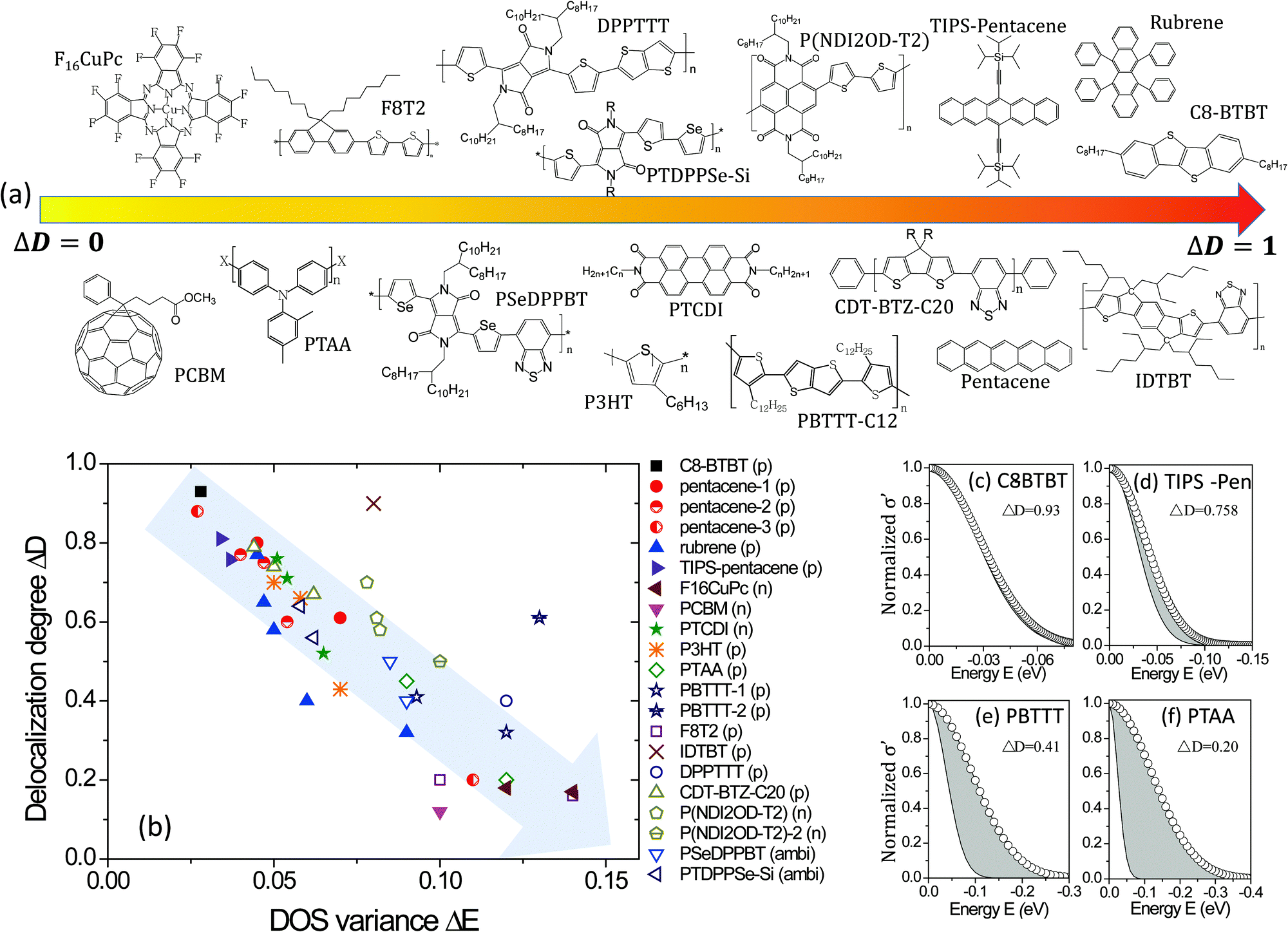
The values used for ΔE and ΔD of the various materials are compared in Fig. 5. Small molecules are drawn in filled dots and polymers are in open dots or lines, of which the polarity of carriers is given after the materials’ name. It is worth noting that the GER gives a unified description for the transition from a negative temperature coefficient of the mobility (dμ/dT < 0) to a positive coefficient (dμ/dT > 0), as shown in TIPS-pentacene crystals, of which ΔD is around 0.80. It is highly consistent with and gives a quantitative explanation to the previous report which shows that the band-like temperature dependence is not due to extended-state conduction but to localized transport limited by thermal lattice fluctuations.21a In addition, from the mapping, it can be directly and clearly seen how the crystallization, dielectric materials, or device structures induce different charge transport disorder for the same OSC, and it can also provide comparisons in charge transport among different OSCs with different crystallinities. The small molecule rubrene crystals with different dielectrics feature distinct transport properties. This has been explained in terms of the tunable small polarons7a and here it can be quantified that high-k dielectrics noticeably decrease the delocalization degree ΔD from 0.77 (parylene) to 0.32 (Ta2O5) and slightly broaden the DOS. Generally, for the same semiconductors with different dielectrics, e.g., TIPS-pentacene, PBTTT, and PTAA, the value of ΔD generally decreases with ΔE. The reason is probably as aforementioned: the DOS variance reflecting energetic disorder is affected by factors such as structural disorders and electronic interaction/coupling between neighboring molecules or polymer chains, which also affect the hopping probability or transfer rate of charges and thus the degree of delocalization.
 |
| | Fig. 5 (a) Schematic representations of materials roughly from a low to high delocalization degree. (b) The values of the delocalization degree ΔD and the DOS variance ΔE are plotted for different semiconductors. The grey arrow shows the direction of increasing disorder in the charge transport. (c–f) The microscopic conductivity and the DOS for some materials, where the grey areas represent the reduced microscopic conductivity owing to the localization of charge transport. | |
Interestingly, now it is possible to use the mapping to compare the transport disorder of semiconductors in different classes of materials. The investigated materials are presented in Fig. 5a roughly in the order from a low to high delocalization degree. It is worth noting that only a few D–A semiconductors exhibit high delocalization degrees, implying there is space for improvement for many D–A semiconductors by presumably optimizing the morphology or dielectric interfaces. Moreover, although thermally evaporated small molecular crystals have higher delocalization degrees and smaller energetic disorders than the solution-processed polymeric semiconductors, solution-cast films can feature very high delocalization degrees, such as C8-BTBT crystals formed by solvent vapor annealing and the polymer indacenodithiophene-co-benzothiadiazole (IDTBT) film deposited by spin-coating. The latter indicates that polymeric semiconductors would not be critically limited by crystallization but can achieve a delocalized degree close to one if they feature a rigid backbone or extended aggregates to build a transport path for intra- and inter-chain or inter-domains,8,38 respectively.
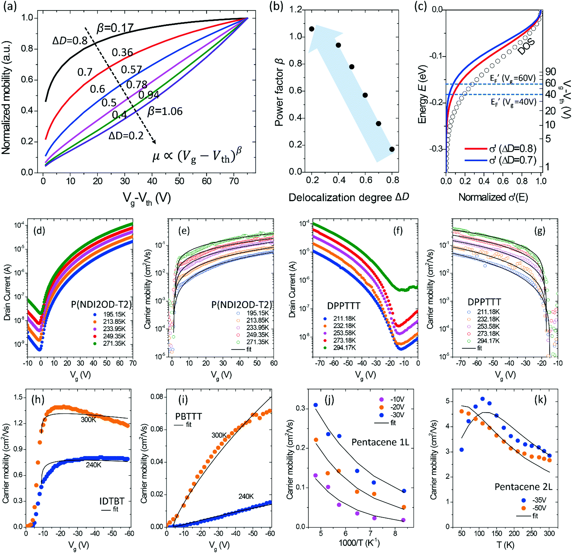
Carrier-concentration-dependent mobility
Besides temperature-dependence, the charge transport mechanism also affects the dependence of carrier mobility on the carrier numbers (n) or the gate voltage (Vg) in FETs, which has also been widely observed and discussed. The dependence of mobility on n or Vg is in fact attributed to the shift of EF mainly tuned by the gate voltage. The relation between n, Vg, and EF is given by:| |  | (8) |
where Ci is the capacitance of the gate dielectric, Vg is the gate voltage, Von is the turn-on voltage, d is the approximate accumulation layer thickness, and the carrier concentration owing to field-effect accumulation is n. We can then calculate EF at different Vg to give the relationship between the charge mobility in the GER. The calculated mobility with varying delocalization degree ΔD is shown in the ESI† (Fig. S6) and the normalized mobility as a function of Vg is shown in Fig. 6a. It can be seen that the widely used power law of mobility μ ∝ (Vg − Vth)β![[thin space (1/6-em)]](https://www.rsc.org/images/entities/char_2009.gif) 39 can describe the cases at which ΔD = 0.2–0.8, while the mobility becomes Vg-independent or even decreases as Vg decreases at a high delocalization degree (ΔD = 0.9 to 1.0). Furthermore, the increased power factor β is related to a more severely attenuated delocalization near the energy gap (decreased ΔD, Fig. 6b), which is in good accordance with previous reports in both theoretical and experimental studies.23 The different μ–Vg relationship originates from the electrostatic doping in OSCs induced by energy level bending by the gate field, which gradually shifts the quasi-Fermi level toward transport levels at the dielectric interface, as shown in Fig. 6c. Apparently, as only the electronic states below EF′ contribute to the channel conductance, OSCs with a smaller ΔD afford a lower overall conductivity at a small Vg, and a shift of EF′ would result in a more obvious change in the overall mobility as compared with those with larger ΔD.
39 can describe the cases at which ΔD = 0.2–0.8, while the mobility becomes Vg-independent or even decreases as Vg decreases at a high delocalization degree (ΔD = 0.9 to 1.0). Furthermore, the increased power factor β is related to a more severely attenuated delocalization near the energy gap (decreased ΔD, Fig. 6b), which is in good accordance with previous reports in both theoretical and experimental studies.23 The different μ–Vg relationship originates from the electrostatic doping in OSCs induced by energy level bending by the gate field, which gradually shifts the quasi-Fermi level toward transport levels at the dielectric interface, as shown in Fig. 6c. Apparently, as only the electronic states below EF′ contribute to the channel conductance, OSCs with a smaller ΔD afford a lower overall conductivity at a small Vg, and a shift of EF′ would result in a more obvious change in the overall mobility as compared with those with larger ΔD.
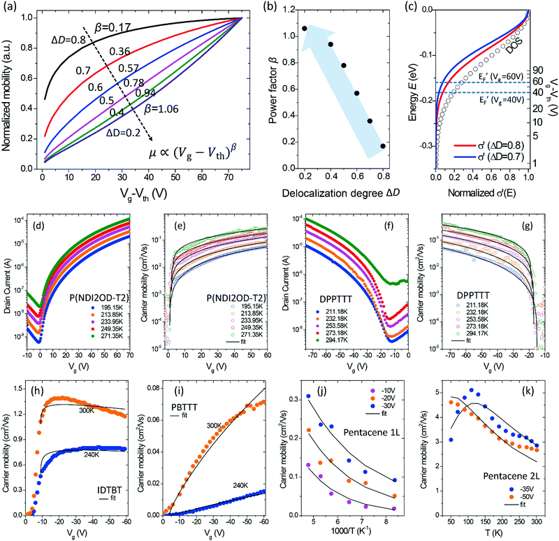 |
| | Fig. 6 (a) The calculated mobility as a function of the gate voltage in the GER for different degrees of delocalization ΔD (ΔE is fixed at 0.1 eV and Ci = 2 × 10⁻⁸ F cm−2). The values of β by fitting are given next to the corresponding curves. (b) The relationship between power factor β and the delocalization degree ΔD. (c) The effect of different gate voltages on the quasi-Fermi energy and the microscopic conductivity. (d–k) Data of mobility as a function of gate voltage for different semiconductor materials at various temperatures (symbols) are fitted by the GER (lines). (d and e) Drain current and extracted mobility for P(NDI2OD-T2), respectively. (f and g) Drain current and extracted mobility for DPPT-TT, respectively. The transistors were measured with VD = 60 V and VD = −80 V, respectively. (h) IDTBT, (i) PBTTT, (j) the first conducting layer (1L) of epitaxial-grown single crystal pentacene, and (k) the second conducting layer (2L). Data were obtained by experimental measurements or from literature.8,40 | |
The above GER calculation is then applied to the experimental data of the Vg-dependence measured from OFETs. Transistors with the n-channel P(NDI2OD-T2) or the p-channel DPP-based copolymer DPPT-TT were fabricated as described in the experimental sections, and the transfer characteristics and the extracted mobility are shown in Fig. 6d–g. For precision, the temperature dependence as well as the Vg-dependence of the mobility are simultaneously fitted by the GER. Despite the simplicity of the calculation method, the same set of parameters of ΔD and ΔE gives a reasonable fitting of the Vg-dependent mobility values at varied temperatures. The values of ΔD and ΔE are listed in Table S3 (ESI†). Also, the recently reported highly planar conjugated polymer IDTBT8 and epitaxial-grown single crystal (pentacene of different layer numbers)40 are investigated by the GER (Fig. 6h–k). IDTBT shows a much higher delocalization degree and a smaller DOS variance (energetic disorder) than PBTTT (see Table S3, ESI†). The results agree well with the thermo-electric and spectroscopic measurements by Venkateshvaran et al.8 In another comparison, the two-layer pentacene crystal exhibits a remarkably higher value of ΔD (0.88) than the one-layer pentacene crystal (ΔD = 0.20). Hence, the GER quantitatively explains the transition from hopping to band-like transport in the different layers of pentacene mainly by the different delocalization degree, which was caused by the different quality and orientation of the crystals in the two layers according to the reports by Zhang et al.40
3. Conclusions
In conclusion, we have presented the GER that characterizes charge transport with a DOS variance factor ΔE and a delocalization factor ΔD. By taking into account the attenuated delocalization at the electronic states near the band edge or the energy gap, we found that it can describe the carrier mobility at variable temperatures, which is predicted by various transport mechanisms. In addition, the GER is capable of describing variable carrier concentrations (various gate voltages in OFETs) of different OSCs from theoretical and experimental aspects. The GER can describe the mobility–temperature behavior and mobility–carrier-concentration dependence predicted by various transport mechanisms in different OSCs. By using the GER to analyze the mobility, we are able to quantitatively compare charge transport properties in the degree of energetic disorder and delocalization, even for different microscopic transport mechanisms and for different classes of OSCs.
4. Experimental section
Fabrication of transistors
Corning Eagle 2000 glass substrates were cleaned sequentially in an ultrasonic bath with de-ionised water, acetone, and isopropanol for 10 min each. The Au/Ni (15 nm/3 nm) source and drain (S/D) patterns were formed by a conventional lift-off photolithography procedure. Materials were synthesized or purchased as described in ref. 11a. The semiconductors were dissolved in 1,2-dichlorobenzene or p-xylene and spin-coated in nitrogen, and the thin films were then thermally annealed at 150 °C for P(NDI2OD-T2) or 250 °C for DPPT-TT, for 30 min. PMMA (Aldrich, Mw = 120 kD) was used as a dielectric material without further purification and was dissolved in n-butyl acetate 80 mg ml−1 and then spin-coated at 2000 rpm for 60 s. After the dielectric-layer coating, the devices were baked at 80 °C for more than 2 hours in a nitrogen glove box. The OFETs were completed by the deposition of an Al gate electrode using a shadow mask.
Characterizations of transistors
The OFET electrical characteristics were measured using a Keithley 4200-SCS parameter analyzer in a nitrogen-filled glove box. The mobility and threshold voltage were calculated in the linear or saturation region using the gradual-channel approximation. C–V characteristics were measured using an Agilent 4284 precision LCR meter and a Keithley 4200-SCS parameter analyzer. For the temperature measurements, the vacuum chamber sealed at ∼10−2 Torr was adjusted to 294–195 K using liquid nitrogen and I–V results were obtained at each temperature.
Acknowledgements
The authors gratefully acknowledge the financial support of the project from the National Natural Science Foundation of China (61504173), Guangdong Provincial Department of Science and Technology (2015B090924001), the Guangdong Natural Science Funds for Distinguished Young Scholars under Grant 2016A030306046, and the Center for Advanced Soft-Electronics (2013M3A6A5073183) funded by the Ministry of Science, ICT & Future Planning. CL & YYN thank Dr Yong Xu for discussions.
References
-
(a) K. Nakayama, Y. Hirose, J. Soeda, M. Yoshizumi, T. Uemura, M. Uno, W. Li, M. J. Kang, M. Yamagishi, Y. Okada, E. Miyazaki, Y. Nakazawa, A. Nakao, K. Takimiya and J. Takeya, Adv. Mater., 2011, 23, 1626 CrossRef CAS PubMed;
(b) C. Liu, T. Minari, X. Lu, A. Kumatani, K. Takimiya and K. Tsukagoshi, Adv. Mater., 2011, 23, 523 CrossRef CAS PubMed;
(c) H. Dong, X. Fu, J. Liu, Z. Wang and W. Hu, Adv. Mater., 2013, 25, 6158 CrossRef CAS PubMed.
-
(a) I. Kang, H.-J. Yun, D. S. Chung, S.-K. Kwon and Y.-H. Kim, J. Am. Chem. Soc., 2013, 135, 14896 CrossRef CAS PubMed;
(b) H.-R. Tseng, H. Phan, C. Luo, M. Wang, L. A. Perez, S. N. Patel, L. Ying, E. J. Kramer, T.-Q. Nguyen, G. C. Bazan and A. J. Heeger, Adv. Mater., 2014, 26, 2993 CrossRef CAS PubMed;
(c) G. Kim, S.-J. Kang, G. K. Dutta, Y.-K. Han, T. J. Shin, Y.-Y. Noh and C. Yang, J. Am. Chem. Soc., 2014, 136, 9477 CrossRef CAS PubMed.
-
(a) Y. Li, P. Sonar, L. Murphy and W. Hong, Energy Environ. Sci., 2013, 6, 1684 RSC;
(b) H. Bronstein, J. M. Frost, A. Hadipour, Y. Kim, C. B. Nielsen, R. S. Ashraf, B. P. Rand, S. Watkins and I. McCulloch, Chem. Mater., 2013, 25, 277 CrossRef CAS;
(c) J. D. Yuen and F. Wudl, Energy Environ. Sci., 2013, 6, 392 RSC.
-
(a) A. Troisi, Chem. Soc. Rev., 2011, 40, 2347 RSC;
(b) R. Noriega, J. Rivnay, K. Vandewal, F. P. V. Koch, N. Stingelin, P. Smith, M. F. Toney and A. Salleo, Nat. Mater., 2013, 12, 1038 CrossRef CAS PubMed.
-
(a) G. Horowitz, J. Mater. Res., 2004, 19, 1946 CrossRef CAS;
(b) A. R. Murphy and J. M. J. Frechet, Chem. Inf., 2007, 38, 1066 Search PubMed;
(c) I. McCulloch, M. Heeney, C. Bailey, K. Genevicius, I. MacDonald, M. Shkunov, D. Sparrowe, S. Tierney, R. Wagner, W. Zhang, M. L. Chabinyc, R. J. Kline, M. D. McGehee and M. F. Toney, Nat. Mater., 2006, 5, 328 CrossRef CAS PubMed.
-
(a) H. Sirringhaus, Adv. Mater., 2014, 26, 1319 CrossRef CAS PubMed;
(b) V. Coropceanu, J. Cornil, D. A. da Silva Filho, Y. Olivier, R. Silbey and J.-L. Brédas, Chem. Rev., 2007, 107, 926 CrossRef CAS PubMed.
-
(a) I. N. Hulea, S. Fratini, H. Xie, C. L. Mulder, N. N. Iossad, G. Rastelli, S. Ciuchi and A. F. Morpurgo, Nat. Mater., 2006, 5, 982 CrossRef CAS PubMed;
(b) H. J. Ding, C. Reese, A. J. Makinen, Z. A. Bao and Y. L. Gao, Appl. Phys. Lett., 2010, 96, 222106 CrossRef;
(c) S. Ciuchi, R. C. Hatch, H. Höchst, C. Faber, X. Blase and S. Fratini, Phys. Rev. Lett., 2012, 108, 256401 CrossRef CAS PubMed.
- D. Venkateshvaran, M. Nikolka, A. Sadhanala, V. Lemaur, M. Zelazny, M. Kepa, M. Hurhangee, A. J. Kronemeijer, V. Pecunia, I. Nasrallah, I. Romanov, K. Broch, I. McCulloch, D. Emin, Y. Olivier, J. Cornil, D. Beljonne and H. Sirringhaus, Nature, 2014, 515, 384 CrossRef CAS PubMed.
-
(a)
S. D. Brotherton, in Introduction to Thin Film Transistors: Physics and Technology of TFTs, Springer International Publishing, Heidelberg, 2013, p. 339 Search PubMed;
(b) J. Y. W. Seto, J. Appl. Phys., 1975, 46, 5247 CrossRef CAS;
(c) J. Levinson, F. R. Shepherd, P. J. Scanlon, W. D. Westwood, G. Este and M. Rider, J. Appl. Phys., 1982, 53, 1193 CrossRef CAS;
(d) A. T. Voutsas, IEEE Trans. Electron Devices, 2003, 50, 1494 CrossRef CAS;
(e) G. Horowitz, Adv. Mater., 1998, 10, 365 CrossRef CAS;
(f) P. G. Le Comber and W. E. Spear, Phys. Rev. Lett., 1970, 25, 509 CrossRef CAS.
-
(a) N. F. Mott, Philos. Mag., 1969, 19, 835 CrossRef CAS;
(b) M. C. J. M. Vissenberg and M. Matters, Phys. Rev. B: Condens. Matter Mater. Phys., 1998, 57, 12964 CrossRef CAS;
(c) S. D. Baranovskii, T. Faber, F. Hensel and P. Thomas, J. Phys.: Condens. Matter, 1997, 9, 2699 CrossRef CAS;
(d)
N. F. Mott and E. A. Davis, Electronic processes in non-crystalline materials, Clarendon Press, 1979 Search PubMed.
-
(a) H. Bässler, Phys. Status Solidi B, 1993, 175, 15 CrossRef;
(b) R. H. Young, Philos. Mag. B, 1995, 72, 435 CrossRef CAS;
(c) R. Schmechel, Phys. Rev. B: Condens. Matter Mater. Phys., 2002, 66, 235206 CrossRef.
- S. Lee, K. Ghaffarzadeh, A. Nathan, J. Robertson, S. Jeon, C. Kim, I.-H. Song and U.-I. Chung, Appl. Phys. Lett., 2011, 98, 203508 CrossRef.
-
(a) J. Yin, R.-F. Chen, S.-L. Zhang, H.-H. Li, G.-W. Zhang, X.-M. Feng, Q.-D. Ling and W. Huang, J. Phys. Chem. C, 2011, 115, 14778 CrossRef CAS;
(b) R. A. Marcus, J. Chem. Phys., 1956, 24, 966 CrossRef CAS;
(c) R. A. Marcus, Rev. Mod. Phys., 1993, 65, 599 CrossRef CAS;
(d) I. Yavuz, B. N. Martin, J. Park and K. N. Houk, J. Am. Chem. Soc., 2015, 137, 2856 CrossRef CAS PubMed.
- K. Asadi, A. J. Kronemeijer, T. Cramer, L. Jan Anton Koster, P. W. M. Blom and D. M. de Leeuw, Nat. Commun., 2013, 4, 1710 CrossRef PubMed.
-
(a) N. J. van der Kaap, I. Katsouras, K. Asadi, P. W. M. Blom, L. J. A. Koster and D. M. de Leeuw, Phys. Rev. B: Condens. Matter Mater. Phys., 2016, 93, 140206 CrossRef;
(b) G. Nan, X. Yang, L. Wang, Z. Shuai and Y. Zhao, Phys. Rev. B: Condens. Matter Mater. Phys., 2009, 79, 115203 CrossRef;
(c) Y. Jiang, Q. Peng, H. Geng, H. Ma and Z. Shuai, Phys. Chem. Chem. Phys., 2015, 17, 3273 RSC.
-
(a) Y. Jiang, X. Zhong, W. Shi, Q. Peng, H. Geng, Y. Zhao and Z. Shuai, Nanoscale Horiz., 2016, 1, 53 RSC;
(b) H. Geng, Q. Peng, L. Wang, H. Li, Y. Liao, Z. Ma and Z. Shuai, Adv. Mater., 2012, 24, 3568 CrossRef CAS PubMed.
- Y. Roichman and N. Tessler, Appl. Phys. Lett., 2002, 80, 1948 CrossRef CAS.
- L. Li, N. Lu and M. Liu, J. Appl. Phys., 2014, 116, 164504 CrossRef.
-
(a) D. Khim, Y. Xu, K.-J. Baeg, M. Kang, W.-T. Park, S.-H. Lee, I.-B. Kim, J. Kim, D.-Y. Kim, C. Liu and Y.-Y. Noh, Adv. Mater., 2016, 28, 518 CrossRef CAS PubMed;
(b) Y. Xu, M. Benwadih, R. Gwoziecki, R. Coppard, T. Minari, C. Liu, K. Tsukagoshi, J. Chroboczek, F. Balestra and G. Ghibaudo, J. Appl. Phys., 2011, 110, 104513 CrossRef.
- L. Wang, G. Nan, X. Yang, Q. Peng, Q. Li and Z. Shuai, Chem. Soc. Rev., 2010, 39, 423 RSC.
-
(a) T. Sakanoue and H. Sirringhaus, Nat. Mater., 2010, 9, 736 CrossRef CAS PubMed;
(b) V. Podzorov, E. Menard, A. Borissov, V. Kiryukhin, J. A. Rogers and M. E. Gershenson, Phys. Rev. Lett., 2004, 93, 086602 CrossRef CAS PubMed;
(c) N. A. Minder, S. Ono, Z. Chen, A. Facchetti and A. F. Morpurgo, Adv. Mater., 2012, 24, 503 CrossRef CAS PubMed.
- W. C. Germs, K. Guo, R. A. J. Janssen and M. Kemerink, Phys. Rev. Lett., 2012, 109, 016601 CrossRef PubMed.
- A. J. Kronemeijer, V. Pecunia, D. Venkateshvaran, M. Nikolka, A. Sadhanala, J. Moriarty, M. Szumilo and H. Sirringhaus, Adv. Mater., 2014, 26, 728 CrossRef CAS PubMed.
- D. Knipp, R. A. Street and A. R. Völkel, Appl. Phys. Lett., 2003, 82, 3907 CrossRef CAS.
- H. Sirringhaus, T. Sakanoue and J.-F. Chang, Phys. Status Solidi B, 2012, 249, 1655 CrossRef CAS.
- R. J. Chesterfield, J. C. McKeen, C. R. Newman, P. C. Ewbank, D. A. da Silva Filho, J.-L. Brédas, L. L. Miller, K. R. Mann and C. D. Frisbie, J. Phys. Chem. B, 2004, 108, 19281 CrossRef CAS.
- J. Lee, A. R. Han, H. Yu, T. J. Shin, C. Yang and J. H. Oh, J. Am. Chem. Soc., 2013, 135, 9540 CrossRef CAS PubMed.
- Y. Yamashita, F. Hinkel, T. Marszalek, W. Zajaczkowski, W. Pisula, M. Baumgarten, H. Matsui, K. Müllen and J. Takeya, Chem. Mater., 2016, 28, 420 CrossRef CAS.
- J.-F. Chang, H. Sirringhaus, M. Giles, M. Heeney and I. McCulloch, Phys. Rev. B: Condens. Matter Mater. Phys., 2007, 76, 205204 CrossRef.
- H. Sirringhaus, M. Bird and N. Zhao, Adv. Mater., 2010, 22, 3893 CrossRef CAS PubMed.
- M. Caironi, M. Bird, D. Fazzi, Z. Chen, R. Di Pietro, C. Newman, A. Facchetti and H. Sirringhaus, Adv. Funct. Mater., 2011, 21, 3371 CrossRef CAS.
- A. J. Kronemeijer, E. Gili, M. Shahid, J. Rivnay, A. Salleo, M. Heeney and H. Sirringhaus, Adv. Mater., 2012, 24, 1558 CrossRef CAS PubMed.
- S. Yadav, P. Kumar and S. Ghosh, Appl. Phys. Lett., 2012, 101, 193307 CrossRef.
- T. D. Anthopoulos, D. M. d. Leeuw, E. Cantatore, P. v. t. Hof, J. Alma and J. C. Hummelen, J. Appl. Phys., 2005, 98, 054503 CrossRef.
- S. F. Nelson, Y.-Y. Lin, D. J. Gundlach and T. N. Jackson, Appl. Phys. Lett., 1998, 72, 1854 CrossRef CAS.
- H. Sirringhaus, R. J. Wilson, R. H. Friend, M. Inbasekaran, W. Wu, E. P. Woo, M. Grell and D. D. C. Bradley, Appl. Phys. Lett., 2000, 77, 406 CrossRef CAS.
- J. Veres, S. D. Ogier, S. W. Leeming, D. C. Cupertino and S. Mohialdin Khaffaf, Adv. Funct. Mater., 2003, 13, 199 CrossRef CAS.
- S. G. Bucella, A. Luzio, E. Gann, L. Thomsen, C. R. McNeill, G. Pace, A. Perinot, Z. Chen, A. Facchetti and M. Caironi, Nat. Commun., 2015, 6, 8394 CrossRef CAS PubMed.
- G. Horowitz, M. E. Hajlaoui and R. Hajlaoui, J. Appl. Phys., 2000, 87, 4456 CrossRef CAS.
- Y. Zhang, J. Qiao, S. Gao, F. Hu, D. He, B. Wu, Z. Yang, B. Xu, Y. Li, Y. Shi, W. Ji, P. Wang, X. Wang, M. Xiao, H. Xu, J.-B. Xu and X. Wang, Phys. Rev. Lett., 2016, 116, 016602 CrossRef PubMed.
Footnote |
| † Electronic supplementary information (ESI) available. See DOI: 10.1039/c7mh00091j |
|
| This journal is © The Royal Society of Chemistry 2017 |
Click here to see how this site uses Cookies. View our privacy policy here. 
 Open Access Article
 This Open Access Article is licensed under a Creative Commons Attribution-Non Commercial 3.0 Unported Licence
 *b
*b


 for different temperatures with low or high delocalization degrees (ΔD = 0.5 or ΔD = 1). The temperatures are varied from T = 100 K up to 370 K (ΔE = 0.1 eV, EF = −0.2 eV). (f) and (g) The effective mobility as a function of temperature for various ΔD (ΔE = 0.20 and 0.06 eV, respectively; EF is fixed at −0.2 eV). The effective mobility decreases as the temperature increases at ΔD = 1, which is consistent with band-like transport.
 is plotted against energy E in Fig. 2d and e. When the temperatures are varied from T = 100 K up to 370 K, the maximum of
  increases homogeneously as the temperature increases in the case when ΔD = 0.5, and so does the overall conductivity (Fig. 2d). In comparison, in the case when ΔD = 1, the maximum of
  decreases as the temperature increases and the change in the overall conductivity becomes much smaller (Fig. 2e). The relationship between the mobility μ and the temperature T (μ–T relation) is then calculated in Fig. 2f and g, where the mobility at a certain temperature with varying ΔD or vice versa can be directly read. At a certain temperature, a larger DOS variance ΔE or a smaller delocalization degree ΔD results in a decreased mobility, which is highly consistent with the above physical understanding. As the temperature decreases, the mobility degrades sharply (or raises slightly) with a low (or high) delocalization degree, which is consistent with the transport mechanism being highly limited by thermal activation (or by lattice/phonon scattering). Importantly, the GER can explain the transition from the band-like temperature dependence of the mobility (i.e., dμ/dT < 0) to the thermally activated temperature dependence (i.e., dμ/dT > 0), which has been reported in some high mobility semiconductors in previous experiments21 and will be discussed below.
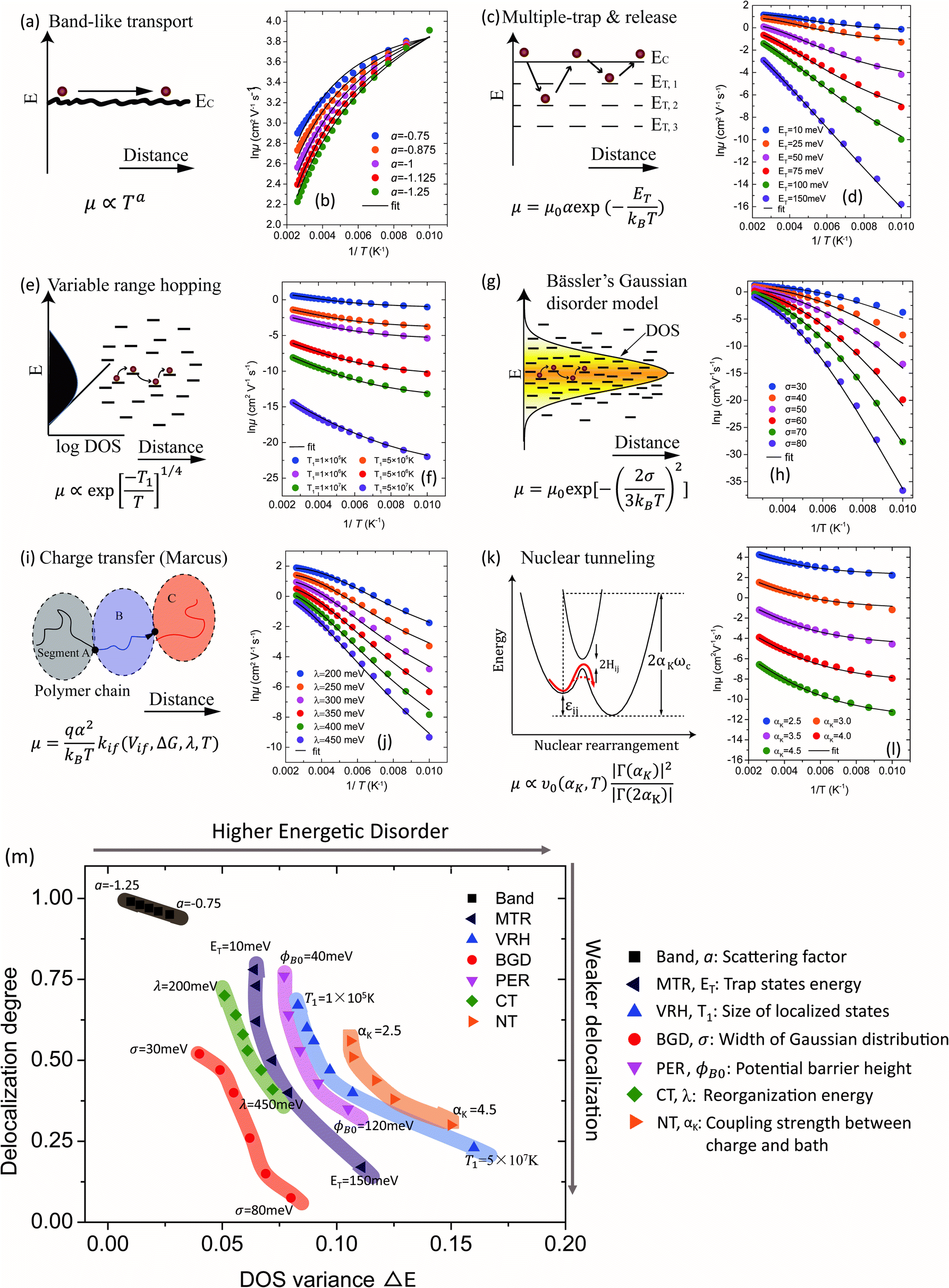
 , where α is the size of the localized state and NF is the density of states at the Fermi edge. In all of the cases, ΔE increases and ΔD decreases as those limiting factors increase, which is consistent with the physical mechanisms of these models. The DOS variance ΔE can be taken as a signature of energetic disorder, as it generally follows the energy disorder parameters in the different models, for example, T1 in the VRH model is proportional to the Urbach energy.23 By gathering all of the fitting values together in Fig. 3m, the impacts of different limiting factors in the various mechanisms of charge transport can now be quantitatively compared under the same axes constructed by ΔE and ΔD. Note that the CT model describes charge transport as being relatively concentrated in a low-disorder and high-delocalization area, while Bässler's Gaussian disorder (BGD) model covers the range in relatively lower degrees of delocalization. This is probably because the CT model mainly describes charge transport for polycrystalline polymers with a long conjugation length and short localized segments, while BGD is proposed for amorphous semiconductors where hopping among localized states is the main process.