
Tailoring metal halide perovskites through metal substitution: influence on photovoltaic and material properties†
Matthew T.
Klug
ab,
Anna
Osherov
ck,
Amir A.
Haghighirad
b,
Samuel D.
Stranks
cd,
Patrick R.
Brown
e,
Sai
Bai
bf,
Jacob T.-W.
Wang
b,
Xiangnan
Dang
 g,
Vladimir
Bulović
ch,
Henry J.
Snaith
*b and
Angela M.
Belcher
*gij
g,
Vladimir
Bulović
ch,
Henry J.
Snaith
*b and
Angela M.
Belcher
*gij
aDepartment of Mechanical Engineering, Massachusetts Institute of Technology, Cambridge, Massachusetts 02139, USA
bDepartment of Physics, University of Oxford, Clarendon Laboratory, Parks Road, Oxford OX1 3PU, UK. E-mail: henry.snaith@physics.ox.ac.uk
cThe Research Laboratory of Electronics, Massachusetts Institute of Technology, Cambridge, Massachusetts 02139, USA
dCavendish Laboratory, JJ Thomson Avenue, Cambridge CB3 0HE, UK
eDepartment of Physics, Massachusetts Institute of Technology, Cambridge, Massachusetts 02139, USA
fBiomolecular and Organics Electronics, IFM, Linköping University, Linköping 58183, Sweden
gDepartment of Materials Science and Engineering, Massachusetts Institute of Technology, Cambridge, Massachusetts 02139, USA
hDepartment of Electrical Engineering and Computer Science, Massachusetts Institute of Technology, Cambridge, Massachusetts 02139, USA
iDepartment of Biological Engineering, Massachusetts Institute of Technology, Cambridge, Massachusetts 02139, USA
jThe Koch Institute for Integrative Cancer Research, Massachusetts Institute of Technology, Cambridge, Massachusetts 02139, USA. E-mail: belcher@mit.edu
kCenter for Materials Science and Engineering, Massachusetts Institute of Technology, Cambridge, Massachusetts 02139, USA
First published on 8th December 2016
Abstract
We present herein an experimental screening study that assesses how partially replacing Pb in methylammonium lead triiodide perovskite films with nine different alternative, divalent metal species, B′ = {Co, Cu, Fe, Mg, Mn, Ni, Sn, Sr, and Zn}, influences photovoltaic performance and optical properties. Our findings indicate the perovskite film is tolerant to most of the considered homovalent metal species with lead–cobalt compositions yielding the highest power conversion efficiencies when less than 6% of the Pb2+ ions are replaced. Through subsequent materials characterisation, we demonstrate for the first time that partially substituting Pb2+ at the B-sites of the perovskite lattice is not restricted to Group IV elements but is also possible with at least Co2+. Moreover, adjusting the molar ratio of Pb:Co in the mixed-metal perovskite affords new opportunities to tailor the material properties while maintaining stabilised device efficiencies above 16% in optimised solar cells. Specifically, crystallographic analysis reveals that Co2+ incorporates into the perovskite lattice and increasing its concentration can mediate a crystal structure transition from the cubic to tetragonal phase at room-temperature. Likewise, Co2+ substitution continually modifies the perovskite work function and band edge energies without either changing the band gap or electronically doping the intrinsic material. By leveraging this orthogonal dimension of electronic tunability, we achieve remarkably high open-circuit voltages up to 1.08 V with an inverted device architecture by shifting the perovskite into a more favourable energetic alignment with the PEDOT:PSS hole transport material.
Broader contextRecent advances in the efficiency of lead-based perovskite photovoltaics towards the 25% achievable by record-setting crystalline silicon solar cells have been realised by tailoring the composition of the organic and halide ions in the material. While this approach of compositional engineering has yielded materials that display a rich array of material properties, it remains largely unexplored how replacing a portion of the lead content in perovskite films with alternative metal species impacts material properties and photovoltaic performance. This is relevant given that crystalline silicon, which currently dominates the photovoltaic market, is especially sensitive to metal impurities and requires elaborate fabrication procedures to produce high-purity material. By experimentally screening through a large set of mixed-metal perovskite compositions, we find that the perovskite film is remarkably tolerant of many extrinsic, homovalent metal species and can maintain competitive photovoltaic performance when less than about 3% of the Pb2+ ions are replaced, which is a content several orders of magnitude higher than the tolerance of silicon. Furthermore, we have identified Co2+ as capable of partially substituting Pb2+ in the crystal lattice and demonstrate this supplies new dimensions of electronic and crystallographic tunability, which we leverage to improve photovoltaic performance in perovskite solar cells. |
Introduction
The rapid rise in performance of lead-based metal halide perovskite solar cells over the past seven years from an initial 3.8% efficiency1 to a recent value of 22.1%2 places this nascent class of materials on par with other commercial solar materials such as cadmium telluride (CdTe) and copper indium gallium selenide (CIGS).3 This achievement coupled with initial reports demonstrating little to no performance degradation over extended outdoor testing4 indicates that perovskite solar cells are quickly approaching a maturity level ripe for commercialisation. An attractive feature of metal halide perovskites is that key material properties can be tailored by engineering the ionic composition of the ABX3 lattice (Fig. 1a). For instance, the band gap of perovskite materials can be tuned throughout a significant portion of the visible and near-infrared spectrum with mixed-halide5–11 systems that vary the content at the X-site. This affords the opportunity to develop even higher efficiency multi-junction solar cells based on stacks of multiple perovskite materials or the pairing of perovskites with current solar technologies such as crystalline silicon (c-Si) or CIGS.12–14 Likewise, the thermal stability and photo-stability of lead-based perovskites can be improved by exchanging the conventional methylammonium cation at the A-site of the perovskite lattice with formamidinium,5 caesium,15 or mixtures10,16–18 of these. This approach of compositional engineering has produced breakthrough perovskite devices with remarkably high efficiencies by blending ions at both the A-site and X-site to form mixed-cation lead mixed-halide materials.10,18,19 In contrast, it remains largely unknown how partially substituting Pb2+ with alternative metal species at the B-site influences material properties and photovoltaic performance. The introduction of certain heterovalent metal ions in perovskite films has been recently shown to influence either their optoelectronic or crystallographic properties. For instance, the incorporation of Bi3+ into MAPbBr3 is capable of narrowing the bandgap and increasing conductivity through electronic doping,20 whereas In3+ and alkali metals (e.g., Na+ and K+) beneficially influence the film morphology and crystallinity of MAPbI3.21,22 Likewise, Al3+ introduction has been shown to decrease the non-radiative recombination rate and improve crystal quality by reducing microstrain in the MAPbI3 lattice.23 However, reports of the homovalent substitution of Pb2+ with a second divalent species are limited. To date, only Sn2+ has been definitively shown to replace a portion of Pb2+ ions at the lattice B-sites, which results in band gap narrowing.24–26 Mixed-cation, mixed-metal perovskites with a 3Pb:2Sn molar ratio have recently achieved efficiencies up to 15.1%.27 However, one of the major drawbacks of Sn is that Sn2+ readily oxidises to Sn4+ upon exposure to air, which causes the perovskite to destabilise into multiple phases, thereby damaging photovoltaic performance.28 Furthermore, a recent toxicology study reveals that Sn-based perovskites also pose serious health risks through environmental acidification that arises during degradation.29 Therefore, it remains an attractive pursuit to identify alternative divalent metal species that are capable of tuning the material properties of the perovskite and preserving its excellent optoelectronic properties without exacerbating the stability or toxicity of the inherent material. As is indicated by Fig. 1b, many of the alkaline earth and transition metals can achieve a stable divalent oxidation state and are compatible with solution-processing, which makes them also suitable candidate species for generating new mixed-metal perovskite compositions. Some of these elements, such as Cu and Fe,30–33 have been used in two-dimensional (2D) layered perovskite structures, and three-dimensional (3D) perovskites that incorporate Cu2+, Ca2+, Cd2+, and Sr2+ into MAPbI3 films have been recently reported.34–36 Although B-site substitution was not achieved, incorporating Sr2+ into MAPbI3 films has yielded remarkably long carrier lifetimes and devices with fill-factors reaching 85%.36 This finding highlights the exciting prospect that perovskites displaying improved optoelectronic properties or interesting new behaviours will emerge by rationally mining the largely unexplored field of alternative mixed-metal compositions.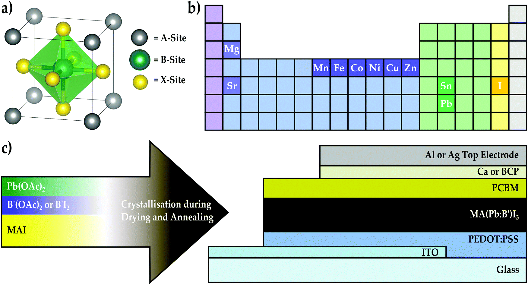 | ||
| Fig. 1 (a) Schematic of the ABX3 perovskite crystal structure. (b) Elements that are used as ions in the mixed-metal perovskite materials. (c) Mixed-metal perovskite materials are integrated into an inverted device architecture using a one-step method where methylammonium iodide (MAI), lead acetate (Pb(OAc)2), and a second divalent metal salt (B′(OAc)2 or B′I2) are dissolved in DMF, the solution is spin-coated onto PEDOT:PSS, and the perovskite is crystallised by drying and annealing the film. | ||
To investigate the opportunities available with alternative mixed-metal perovskite compositions, we present a feasibility screening study where between 1.6% and 25% of the Pb-content has been replaced with a second divalent metal species to form methylammonium mixed-metal triiodide films, denoted here as MA(Pb:B′)I3 where B′ = {Co, Cu, Fe, Mg, Mn, Ni, Sn, Sr, and Zn}. The present work is the first report that systematically replaces a fraction of the Pb content in 3D perovskite films with transition metals. By experimentally screening through this large set of alternative metals and benchmarking mixed-metal perovskite films against the MAPbI3 baseline material, we investigate how tolerant the photovoltaic performance of MAPbI3 devices is to the introduction of a second metal species and characterise the material and electronic properties of several mixed-metal perovskite compositions to elucidate the mechanisms responsible for observed trends in relative performance. The purpose of this screening study is to identify alternative metal species that promise to augment the properties of metal halide perovskites while preserving their remarkable optoelectronic qualities. We prove the suitability of the most-promising series of mixed-metal compositions to state-of-the-art devices by optimising their deposition to maximise photovoltaic performance. By systematically replacing different amounts of the lead content with a secondary metal species, we find that, compared to Si,37,38 the MAPbI3 lattice is remarkably tolerant of many extrinsic homovalent species and that the excellent electronic properties of the lead-based perovskite are perturbed but not completely disrupted, allowing certain compositions to generate improvements in relative photovoltaic performance. Specifically, we found that MAPbI3 is most tolerant to Co, Cu, Sn, and Zn, and device performance can often be improved upon modest levels of replacement, with a 63Pb:1Co molar ratio yielding a champion performance of 17.2% in optimised solar cells. Subsequent investigation of the electronic properties of the Pb:Co perovskite series reveals that introducing Co into the MAPbI3 material shifts the Fermi and band edge energies without modifying the material band gap. Furthermore, crystallographic analysis reveals that Co2+ is able to occupy the B-site of the perovskite lattice and can mediate the transition of the crystal phase from cubic to tetragonal at room temperature, giving strong evidence that successful B-site substitution of the perovskite lattice can occur with species outside the Group IV elements. These findings demonstrate that transition metal substitution provides new dimensions for tuning the electronic and crystallographic properties of perovskite materials while maintaining efficient photovoltaic performance.
Results and discussion
As illustrated in Fig. 1c, the perovskite solar cells were fabricated using acetate salts as the metal precursors39 and the inverted planar device configuration, where the perovskite is deposited on the hole transporter poly(3,4-ethylenedioxythiophene):poly(styrene-sulfonate) (PEDOT:PSS)40,41 and a fullerene derivative is used as an electron transporter layer. Inverted devices exhibit minimal hysteresis effects,40,41 so this configuration was chosen to eliminate the device architecture itself as a source of hysteresis in the event that mixed-metal devices displayed such behaviour in the current–voltage characteristics. Divalent metal acetates, B(OAc)2, were chosen as the metal precursor materials because most acetate salts, with the exception of calcium and strontium, are soluble in dimethylformamide (DMF) and lead acetate produces remarkably smooth perovskite films.39 As is represented by the schematic in Fig. 1c, most mixed-metal perovskite films were synthesised in a one-step process by spin-coating a solution containing methylammonium iodide (MAI), Pb(OAc)2, and B′(OAc)2 in DMF with a 3![[thin space (1/6-em)]](https://www.rsc.org/images/entities/char_2009.gif) :1 molar ratio of MAI to total metal acetate content. The one exception to this method was strontium, where a 3:1 molar ratio of MAI:Pb(OAc)2 was blended with a 1:1 molar ratio of MAI:SrI2 due to the poor solubility of Sr(OAc)2 in DMF. To build the inverted device architecture, the perovskite solution was spin-coated on an indium tin oxide (ITO) substrate coated with a PEDOT:PSS layer and crystallised by drying and annealing the film. This was followed by sequentially spin-coating and heat-treating a layer of the n-type fullerene derivative, phenyl-C61-butyric acid methyl ester (PCBM), and depositing either Ca/Al or bathocuproine (BCP)/Ag as the interlayer/electrode material pair.
:1 molar ratio of MAI to total metal acetate content. The one exception to this method was strontium, where a 3:1 molar ratio of MAI:Pb(OAc)2 was blended with a 1:1 molar ratio of MAI:SrI2 due to the poor solubility of Sr(OAc)2 in DMF. To build the inverted device architecture, the perovskite solution was spin-coated on an indium tin oxide (ITO) substrate coated with a PEDOT:PSS layer and crystallised by drying and annealing the film. This was followed by sequentially spin-coating and heat-treating a layer of the n-type fullerene derivative, phenyl-C61-butyric acid methyl ester (PCBM), and depositing either Ca/Al or bathocuproine (BCP)/Ag as the interlayer/electrode material pair.
Instead of individually optimising each of the 45 considered mixed-metal compositions, a feasibility study was performed to screen through the full set and (1) provide an initial assessment of how each of the nine secondary metal species influences photovoltaic performance and optical properties, and (2) identify the most promising series for further device optimisation and materials characterisation. While the details of the screening study are discussed in part II of the ESI,† there are several general observations that can be distilled from comparing the average performance metrics of the mixed-metal devices relative to the baseline obtained from neat Pb devices (Fig. S1, ESI†): (1) performance is maintained and can even be improved upon replacing a small fraction of Pb (63Pb:1B′ molar ratio, denoted here as MA(63Pb:1B′)I3) with a second metal species. (2) With the exceptions of Sn and Cu, further increases in the B′ mole fraction is eventually accompanied by a substantial decrease in the photocurrent, which concomitantly reduces the PCE. The metal fraction where this drop occurs provides an empirical measure of the tolerance of MAPbI3 to each species, which is generally around a 15Pb:1B′ molar ratio with Co, Cu, Sn, and Zn being the most tolerated. (3) In contrast, Fe is the only alternative metal species whose inclusion in the perovskite is always detrimental to performance, even at the lowest Fe fraction considered.
Each mixed-metal composition was characterised using spectrophotometry and steady-state photoluminescence (PL) to assess how the considered secondary metal species affect the optical properties of the perovskite film. The full data set for each material composition is reported in the ESI† with absorbance and steady-state PL emission spectra in Fig. S15–S17 (ESI†) with tabulated peak locations in Table S7 (ESI†). The external quantum efficiency (EQE) spectrum was also measured for devices constructed from each mixed-metal composition in order to evaluate how efficiently photocurrent is generated at different wavelengths and to provide an additional measure of material band gap from the onset of photocurrent generation (Fig. S19 and S20, ESI†). Consistent with other reports,24–26,42 band gap narrowing occurs in the Pb:Sn mixtures as is evidenced by the EQE spectra plotted in Fig. 2a, which shows current generation occurring progressively deeper into the infrared region as the Sn content is increased. These plots reveal that mixtures with a Sn fraction at or below 15Pb:1Sn do not show any band gap shift and maintain the 1.56 eV of MAPbI3. However, the band gap narrows continually as the Sn fraction is increased with 7Pb:1Sn, 3Pb:1Sn, and 1Pb:1Sn mixtures yielding respective values of 1.41, 1.31, and 1.24 eV. Similar plots of the EQE edge reveal that Pb:Fe, Pb:Mg, Pb:Ni, and Pb:Sr only yield slightly widened band gaps (<0.09 eV difference from MAPbI3) for 7Pb:1B′ and 3Pb:1B′ mixtures (Fig. S20 and Table S8, ESI†). These findings are consistent with a recent study of Pb:Sr blends, which also reports no change in absorbance edge for low levels of Sr replacement (<5% molar).36 In contrast to Sn, Fig. 2b demonstrates that introducing Co into the perovskite does not shift the EQE edge at any Pb:Co ratio, which also largely holds true for mixtures of Pb:Cu, Pb:Mn, and Pb:Zn (Fig. S20 and Table S8, ESI†). These trends are also observed in the position of the PL emission peaks and the absorption edges presented in Fig. S15–S17 (ESI†). While band gap narrowing with Sn provides an opportunity to move beyond the p–i–n device architecture presented here towards multi-junction architectures,43 the band gap remains relatively stable when the perovskite film is perturbed with any of the other secondary metal species considered. This suggests that, unlike Sn, most of these metals do not significantly modify the character of the band edges at levels below 25% molar replacement.44,45
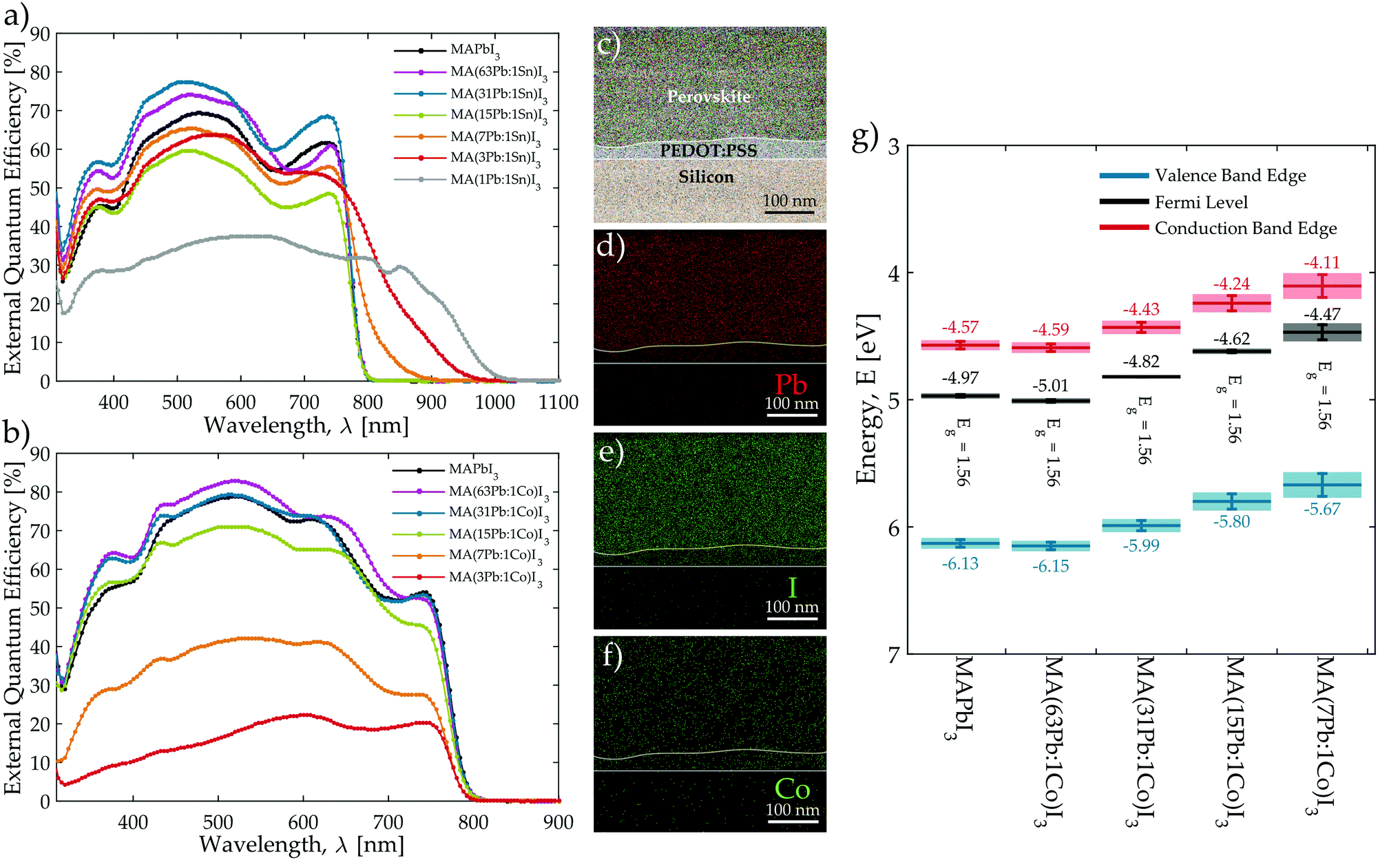 | ||
| Fig. 2 External quantum efficiency for representative (a) MA(Pb:Sn)I3 and (b) MA(Pb:Co)I3 solar cells. (c) STEM image of TEM cross-section milled from MA(31Pb:1Co)I3 film with a focused ion beam. Each layer is identified from the composite elemental maps performed with EDX in STEM mode, which provides the false colour. Individual elemental maps of (d) Pb, (e) I, and (f) Co indicate that the elements are distributed homogeneously throughout the film thickness. (g) Energy levels of the MA(Pb:Co)I3 materials relative to the vacuum level. The Fermi and valence band edge (VBE) energies were determined directly from ultraviolet photoelectron spectroscopy and the conduction band edge (CBE) energies were inferred using the band gap values determined from the edge of the external quantum efficiency (EQE) spectra. | ||
Of the metals investigated, the Fe series of mixed-metal blends yielded the lowest performing solar cells, whereas the Co series produced the highest. An explanation for the diminished performance of the Fe series lies in the observation that the PL intensity for each Pb:Fe blend is two orders of magnitude lower than the MAPbI3 control (Fig. S21, ESI†). This suggests that an abundance of non-radiative recombination is occurring within the perovskite layer, which is consistent with the dramatic reductions in photocurrent observed with all Pb:Fe compositions (Fig. S1b, ESI†). It has been reported that the introduction of Fe into silicon solar cells is also detrimental to performance, as interstitial Fe produces deep level traps in the band gap and has a large electron capture cross-section.37 Although further characterisation is required, it is possible that Fe behaves similarly in perovskite systems.
The Pb:Co blends were chosen from the set of mixed-metals for further investigation with specialised characterisation techniques because they displayed the highest device efficiencies at low levels of Pb replacement (<6% molar). The spatial distribution of elements throughout the thickness of MA(31Pb:1Co)I3 was assessed by milling a TEM cross-section from a film and examining it with energy-dispersive X-ray spectroscopy (EDX). Fig. 2c presents a scanning transmission electron micrograph (STEM) of the cross-section with an overlaid composite EDX map, which clearly identifies the silicon substrate, PEDOT:PSS layer, and perovskite film by colour. Individual elemental maps of Pb, I, and Co throughout the film cross-section are shown in Fig. 2d–f, respectively. It is clear that both Pb and Co atoms are evenly dispersed throughout the film thickness. By integrating the counts of the maps for the elements over the film cross-section, the EDX software provides a quantitative assessment of the amount of Pb and Co present in the film. This analysis yields a molar Pb:Co ratio of (96.4):(3.6), which is remarkably close to the expected value of (96.9):(3.1) based on the stoichiometry of the precursor solution. Furthermore, investigation of this composition with X-ray photoelectron spectroscopy (XPS) confirms that cobalt is present in the film as Co2+ whereas Co0 is absent (Fig. S25, ESI†). This evidence provides confidence that the composition of the mixed-metal films preserves the metal stoichiometry of the original precursor solutions.
Films of the MA(Pb:Co)I3 series were further characterised with ultraviolet photoelectron spectroscopy (UPS) measurements to consider how Co2+ introduction influences the Fermi and valence band edge (VBE) energies of the perovskite material. The flat band energies relative to vacuum for each material are plotted in Fig. 2g and the conduction band edge (CBE) energy is obtained by subtracting the band gap, as determined from the EQE edges (Fig. 2b) for each Pb:Co composition, from the VBE energy. The UPS measurements indicate that replacing some of the Pb content with Co significantly influences the band edge energies even though the band gap of the perovskite film does not vary with the molar Pb:Co ratio. As the Co content is increased from 63Pb:1Co to 7Pb:1Co, the energies relative to the vacuum level shift to increasingly shallower energies, but there is only a negligible change in the energy difference between the Fermi and VBE energies with increasing Co content, which indicates that Co2+ is not electronically doping the perovskite. Therefore, introducing Co2+ into the perovskite film provides a means to directly tailor the energetics of the perovskite in a manner that is decoupled from the band gap. We also note that the Voc increases in-step with shifts toward lower work functions as the Co content is increased. Since UPS only probes the first few nanometres of the film surface, we conclude that the presence of Co2+ ions near the surface of the perovskite film modifies the surface dipole and shifts the energetics of the material into a more favourable configuration with PEDOT:PSS (Fig. S26, ESI†), thereby improving the Voc of the corresponding devices. A detailed discussion on how the energetic shifts impact the device physics and photovoltaic performance (Fig. S27) is presented in the ESI.†
In order to demonstrate that the trends in material properties and photovoltaic performance observed in the screening study are applicable to high-efficiency perovskite systems, film optimisation was performed on the MA(Pb:Co)I3 compositions. Following the methodology reported by Zhang et al.,46 the perovskite deposition conditions were optimised to yield a baseline MAPbI3 film morphology (Fig. 3a) consisting of densely-packed grains without pinholes. As is evident from the top-view scanning electron micrographs in Fig. 3b–d, the grain size gradually reduces with increasing Co2+ fraction while the films remain virtually pinhole-free.
 | ||
| Fig. 3 Scanning-electron micrographs of (a) MAPbI3 and (b–d) MA(Pb:Co)I3 films. | ||
Investigation of the optimised MA(Pb:Co)I3 films with powder X-ray diffraction (XRD) (Fig. 4a) reveals that introducing Co2+ into the film modifies the crystal structure of the perovskite lattice. The corresponding crystallographic parameters for each composition as determined through Rietveld refinement are reported in Table 1. At room temperature, the neat MAPbI3 and MA(127Pb:1Co)I3 materials adopt the cubic crystal structure, whereas the materials with higher Co content display the tetragonal phase as evidenced by extra reflections and observable peak splitting into the set of (002tet, 110tet) reflections in Fig. 4a. While a tetragonal crystal structure was previously reported for MAPbI3 films at room temperature using our deposition method on TiO2,46 the films discussed here are instead deposited on PEDOT:PSS and the adoption of a cubic lattice is consistent with recent findings that also use acids to assist film formation on ITO/PEDOT:PSS substrates.47
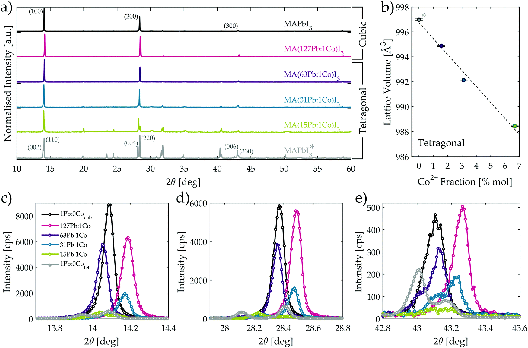 | ||
| Fig. 4 (a) X-ray diffraction spectra of optimised MA(Pb:Co)I3 films. * Corresponds to the reference spectra for a tetragonal MAPbI3 powder ground from a single crystal. (b) Lattice volume as a function of Co2+ fraction for the compositions with tetragonal crystal structure. Local region around the (c) first, (d) second, and (e) third strongest cubic diffraction peaks. The legend shown in (c) is also applicable for (d and e). | ||
| Co [%] | Pb [%] | Material designation | Crystal system | Space group | Lattice parameters [Å] | Unit cell volume [Å3] |
|---|---|---|---|---|---|---|
| 0 | 100 | MAPbI3 | Cubic |
Pm![[3 with combining macron]](https://www.rsc.org/images/entities/char_0033_0304.gif) m m |
a = 6.2842(1) | 248.17 |
| 0.8 | 99.2 | MA(127Pb:1Co)I3 | Cubic |
Pmm |
a = 6.2675(3) | 246.21 |
| 1.6 | 98.4 | MA(63Pb:1Co)I3 | Tetragonal | I4/mcm | a = 8.8845(7), c = 12.6034(5) | 994.86 |
| 3.1 | 96.9 | MA(31Pb:1Co)I3 | Tetragonal | I4/mcm | a = 8.8624(5), c = 12.6134(0) | 992.11 |
| 6.3 | 93.7 | MA(15Pb:1Co)I3 | Tetragonal | I4/mcm | a = 8.8481(9), c = 12.6256(0) | 988.46 |
| 0 | 100 | MAPbI3 | Tetragonal | I4/mcm | a = 8.8703(7), c = 12.6709(5) | 996.99 |
Fig. 4c–e clearly show that each of the three strongest diffraction peaks of the cubic MAPbI3 film are uniformly shifted by nearly 0.1° when 0.8% of the Pb2+ ions are replaced with Co2+ in the MA(127Pb:1Co)I3 composition. As indicated in Table 1, this uniform shift to higher diffraction angles reveals the unit cell contracts, which is consistent with Pb2+ being partially replaced by the smaller sized Co2+ ion at the B-sites of the perovskite lattice. This crystallographic evidence, in conjunction with the homogeneous distribution of Co (Fig. 2f) throughout the perovskite film thickness and the confirmation of Co2+ through XPS (Fig. S25, ESI†), leads us to conclude that Co2+ successfully occupies the lattice B-site. As more of the Pb2+ is further replaced with Co2+, the lattice is forced to distort and adopt the tetragonal crystal phase in order to accommodate the increased strain generated by continued metal substitution. The point of crystal structure transition occurs for the MA(63Pb:1Co)I3 composition as is evidenced by the non-uniform shifting of the diffraction peak positions relative to those of the cubic MAPbI3 material. For instance, the (100) peak (Fig. 4c) displays a greater shift to smaller diffraction angles than the (200) peak (Fig. 4d) and the (300) peak shows signs of splitting into the (006) and (330) peaks of the tetragonal phase with the appearance of a shoulder at 43.0° (Fig. 4e). While both cubic and tetragonal crystal phases are likely present in MA(63Pb:1Co)I3, the tetragonal phase dominates as a better crystallographic fit was obtained with the I4/mcm space group. The crystal phase transition to the tetragonal structure completes with higher Co2+ fractions as is evidenced by clear peak splitting for the MA(31Pb:1Co)I3 and MA(15Pb:1Co)I3 materials in Fig. 4c–e. Furthermore, peak shifts are still observed when the positions of these peaks are compared against a reference sample for a neat MAPbI3 powder obtained from a ground single crystal in the tetragonal crystal phase.48–52Fig. 4b shows the unit cell volume of the tetragonal phases linearly contracts with increasing Co2+ mole fraction and yields a lattice volume shrinkage of 0.86% with the highest considered cobalt content. This clearly indicates the Co2+ ions also substitute into the lattice with the tetragonal crystal structure.
The current–voltage characteristics for the champion solar cells with each composition in the optimised MA(Pb:Co)I3 series is shown in Fig. 5a and the corresponding values for the photovoltaic metrics are tabulated in Table 2. Fig. 5b and Table 2 report the average solar cell performance metrics and clearly indicate that the same performance trends observed in the initial screening study for Pb:Co (Fig. S1 and S2a, ESI†) are now reproduced but with substantially higher efficiencies: (1) as the Co2+ fraction is increased, the Jsc initially remains the same as the neat Pb baseline material until the tolerance limit is reached around 31Pb:1Co, after which the current decreases sharply. (2) The Voc steadily increases with Co content from a mean value of 0.96 V for the baseline up to 1.08 V for the champion 31Pb:1Co cell. (3) The fill-factor does not vary from the baseline value with Co content until the tolerance limit is surpassed, after which it decreases slightly. (4) The 63Pb:1Co blend remains the highest performing composition and exceeds the performance of the MAPbI3 baseline. (5) As shown in Fig. 5a, the current–voltage characteristics hardly display any hysteresis with low Co content. However, the curves display the same behaviour observed in the screening study (Fig. S2a, ESI†), where the hysteresis becomes increasingly pronounced as the Co content is increased.
 | ||
| Fig. 5 (a) Champion forward (right-pointing triangles) and reverse (left-pointing triangles) current–voltage characteristic scans measured from the solar cells optimised for each of the MA(Pb:Co)I3 compositions. (b) Compiled average performance metrics of the optimised MA(Pb:Co)I3 solar cells. Average values and standard deviations for the error bars are calculated from at least 24 different solar cells, spanning at least two separate device batches. The colour scheme in part (b) corresponds to the legend for part (a). | ||
| Co [%] | Pb [%] | Device designation | PCE (%) | J sc mA cm−2 | V oc (V) | FF (%) | SPO (%) |
|---|---|---|---|---|---|---|---|
| 0 | 100 | MAPbI3 | 14.4 ± 1.4 (16.6) | 19.8 ± 1.6 (21.2) | 0.96 ± 0.02 (0.99) | 75.6 ± 2.7 (78.6) | (16.0) |
| 0.8 | 99.2 | MA(127Pb:1Co)I3 | 14.9 ± 0.9 (16.7) | 19.6 ± 0.8 (21.1) | 1.00 ± 0.03 (1.02) | 76.5 ± 3.2 (77.4) | (16.3) |
| 1.6 | 98.4 | MA(63Pb:1Co)I3 | 15.0 ± 0.9 (17.2) | 19.2 ± 0.9 (21.1) | 1.03 ± 0.02 (1.05) | 76.2 ± 3.2 (77.7) | (16.8) |
| 3.1 | 96.9 | MA(31Pb:1Co)I3 | 12.4 ± 1.0 (14.2) | 16.5 ± 1.4 (17.5) | 1.05 ± 0.03 (1.08) | 71.7 ± 4.6 (75.1) | (14.3) |
| 6.3 | 93.7 | MA(15Pb:1Co)I3 | 5.7 ± 0.9 (8.3) | 9.0 ± 1.3 (13.1) | 0.99 ± 0.03 (0.94) | 64.2 ± 6.2 (67.4) | (6.0) |
Lastly, absorbance (Fig. S31, ESI†) and steady state PL measurements (Fig. S32, ESI†) of the optimised MA(Pb:Co)I3 films both confirm that the band gap of the perovskite film does not observably change with Co content. The fact that the optimised Pb:Co blends reproduce the same behaviours observed in both optical properties and photovoltaic performance during the screening study provides confidence that the findings reported for other secondary metal species are likely to remain valid upon further device optimisation. It must also be mentioned that these optimised devices were measured in ambient air and the power output stabilised within seconds of illumination as is indicated by the stabilised power output (SPO) values reported in Table 2 and the time traces in Fig. S29 of the ESI.†
Based on the aggregate of our collected data, we propose the mechanism illustrated in Fig. 6 as an explanation for the performance trends observed in the MA(Pb:Co)I3 mixed-metal compositions. The photovoltaic performance metrics suggest that introducing Co2+ into the perovskite lattice produces two effects whose competition governs the power conversion efficiency, a beneficial one that improves the photovoltage and a detrimental one that reduces the collected photocurrent. The former results from the Co2+ ions shifting the energy levels of the perovskite into a more favourable energetic alignment with PEDOT:PSS, thereby improving the Voc of the device (Fig. S26 and S27, ESI†). Whereas, the latter arises from the Co2+ ions introducing centres for non-radiative recombination that siphon away photocurrent, which is consistent with the observation that PL intensity (Fig. S33, ESI†) and Jsc (Fig. 5b) decrease with increasing Co content. From this perspective, Co might behave similarly to Fe, but to a considerably lesser degree, by either acting as a recombination centre itself or inducing lattice defects that trap charge carriers. The latter is supported by an observed correlation between lattice deformation and optoelectronic quality where the PL intensity initially increases from the neat Pb baseline for the 127Pb:1Co composition and then continually decreases for higher Co2+ fractions (Fig. S33, ESI†), which also corresponds to the point of lattice transition from the cubic to tetragonal phase (Fig. 4a). Although further investigation is required to precisely characterise the nature of these traps, it appears that non-radiative loss is induced by continued Co2+ introduction. When a small amount of Pb2+ is initially substituted with Co2+, there is only a very minor loss in current that is easily outweighed by the improvement in voltage. As more Co2+ is introduced, the voltage continues to rise but the film becomes increasingly less efficient at transporting charges to the selective contacts for collection as more traps are available to intercept and quench charges during migration. Eventually, enough Co2+ ions are present in the film to counteract the benefit arising from energetics, and any further increase in Co2+ fraction only serves to reduce the photocurrent output by increasing the density of recombination centres in the system. As a result, there exists an optimal Pb:Co composition that maximises the PCE where the voltage is increased and the photocurrent is hardly diminished. Although further investigation is required, it is likely that the other transition and alkaline earth metals behave in the same manner as Co since they exhibit similar trends in both photovoltaic performance and material properties in both the screening study and in recent reports.36
 | ||
| Fig. 6 The observed trend in photocurrent, J, for MA(Pb:Co)I3 systems as a function of Co2+ fraction could be explained by the Co2+ ions (violet circles) introducing recombination centres that siphon away current (orange arrows) by trapping photogenerated charge carriers. The presence of Co2+ at the interface between the perovskite and PEDOT:PSS layers initially increases the photovoltage, V, by improving the energetic alignment between these materials. The competition between the detrimental impact of Co2+ on the photocurrent and beneficial impact on the photovoltage explains why the PCE is maximised when an optimal amount of Co2+ is introduced into the system. | ||
There are few reports to date in which inverted solar cells that use PEDOT:PSS and MAPbI3 achieve open-circuit voltages exceeding 1.0 V.40,53,54 An equilibrium diagram of PEDOT:PSS and MAPbI3 based on our UPS measurements (Fig. S27, ESI†) suggests that these devices are operating under a small energetic barrier at the interface, which provides an unfavourable energetic landscape that allows for the injection of electrons into PEDOT:PSS. As is discussed in detail in the ESI,† this leakage current would correlate to a reduced Voc, which might explain why PEDOT:PSS/MAPbI3 devices often achieve lower photovoltages than systems that employ NiOx55 or poly-TPD23,56 as the hole transporter. As Co2+ is introduced into the material, the barrier at the interface decreases until it eventually disappears and the current leakage is reduced, thereby allowing for open-circuit voltages up to 1.08 V to be generated in the devices. Both the optimised MA(Pb:Co)I3 devices (Fig. S30, ESI†) and those produced in the screening study (Fig. S28, ESI†) display reductions in the dark currents with increasing Co content, which supports this explanation. It must be noted that this improvement mechanism in the photovoltage is specific for the combination of PEDOT:PSS and MA(Pb:Co)I3 materials and a separate study is required to investigate the energetics of systems employing different hole transporters or perovskite compositions.
Conclusion
We have performed an experimental screening effort that evaluates how replacing up to 25% of the Pb content in MAPbI3 perovskite films with Sn and eight different transition and alkali earth metal species influences both photovoltaic and optical properties. The photovoltaic performance of MAPbI3 generally tolerates replacing up to 6% of the Pb content with most of the considered extrinsic metal species when our fabrication procedure is used. The notable exception is Fe, which introduces trap states that severely diminish photovoltaic performance and photoluminescence even at relatively low levels of Pb replacement. This aggregate set of data suggests that only Sn is able to appreciably modify the perovskite band gap and preserve device efficiencies when 25% of the Pb is replaced, whereas each of the alkaline earth and divalent transition metal species demonstrates a content limit beyond which the photocurrent decreases precipitously. However, we show for the first time that Sn2+ is not unique, but that Co2+ can also partially replace Pb2+ at the B-sites of the perovskite crystal lattice. At relatively low levels of Pb substitution (<3% molar), the Pb:Co series displays several interesting electronic and crystallographic features while maintaining competitive levels of photovoltaic performance. An optimum molar ratio of 63Pb:1Co reached a champion efficiency of 17.2% by improving the Voc over the baseline MAPbI3 while maintaining the FF and producing only a slightly reduced Jsc. This performance improvement arises from the ability of Co to tune the Fermi level and VBE of the perovskite in a manner that is decoupled from the band gap and shift the material into a more favourable energetic alignment with PEDOT:PSS. Moreover, crystallographic analysis of XRD spectra reveals increasing the Co2+ fraction at the lattice B-sites can controllably induce a crystal structure transition from the cubic to tetragonal phase at room temperature. While, the properties of Pb:Co blends are examined here in detail, it is likely that other species such as Mg2+, Mn2+, Ni2+, and Zn2+ might also behave similarly to Co2+ as they are of comparable ionic size, stable as divalent ions, and do not disrupt photovoltaic performance at low levels of replacement. However, further study is required to optimise their performance, examine their optoelectronic properties, and confirm their ability to partially occupy the lattice B-sites. Our successful incorporation of a transition metal into the MAPbI3 lattice not only provides new dimensions of electronic and crystallographic tunability for current optoelectronic applications, but prepares the way for the emergence of new mixed-metal perovskite compositions that display interesting new physical behaviours.Author contributions
The manuscript was written through contributions of all authors. All authors have given approval to the final version of the manuscript. M. T. K. and A. M. B. conceived the idea. M. T. K., A. O., and S. D. S. designed the experiments. X. D. synthesised and purified the methylammonium iodide precursor. M. T. K. and S. B. fabricated the solar cells and samples for materials characterisation. Current–voltage characteristics and EQE measurements for solar cells were performed by M. T. K. Film thicknesses, absorbance spectra, and steady-state photoluminescence spectra were measured by M. T. K. Scanning electron microscopy were performed by A. O. and J. T.-W. W. TEM cross-section preparation, high-resolution TEM imaging, and EDX elemental mapping, and XPS were performed by A. O. UPS was performed by P. R. B. XRD and crystallographic analysis on optimised Pb:Co materials was performed by A. A. H. The project was supervised by A. M. B., H. J. S., and V. B.Competing financial interest
The Massachusetts Institute of Technology has filed for a patent based on this work.Acknowledgements
This work was supported by Eni, S. p. A. (Italy) through the MIT Energy Initiative Program. S. D. S. acknowledges funding from the People Programme (Marie Curie Actions) of the European Union's Seventh Framework Programme (FP7/2007-2013) under REA grant agreement number PIOF-GA-2013-622630. P. R. B. acknowledges support from the Fannie and John Hertz Foundation and the National Science Foundation. S. B. is a VINNMER Fellow and Marie Skłodowska-Curie Fellow. The authors would like to thank Dr Nakita K. Noel and Dr Alexandra Ramadan for the helpful discussions on this work.References
- A. Kojima, K. Teshima, Y. Shirai and T. Miyasaka, J. Am. Chem. Soc., 2009, 131, 6050–6051 CrossRef CAS PubMed.
- National Renewable Energy Laboratories (NREL) Efficiency Chart, Rev. 01-11-2016, http://www.nrel.gov/ncpv/images/efficiency_chart.jpg.
- S. D. Stranks and H. J. Snaith, Nat. Nanotechnol., 2015, 10, 391–402 CrossRef CAS PubMed.
- X. Li, M. Tschumi, H. Han, S. S. Babkair, R. A. Alzubaydi, A. A. Ansari, S. S. Habib, M. K. Nazeeruddin, S. M. Zakeeruddin and M. Grätzel, Energy Technol., 2015, 3, 551–555 CrossRef CAS.
- G. E. Eperon, S. D. Stranks, C. Menelaou, M. B. Johnston, L. M. Herz and H. J. Snaith, Energy Environ. Sci., 2014, 7, 982 CAS.
- F. Hao, C. C. Stoumpos, D. H. Cao, R. P. H. Chang and M. G. Kanatzidis, Nat. Photonics, 2014, 8, 489–494 CrossRef CAS.
- S. A. Kulkarni, T. Baikie, P. P. Boix, N. Yantara, N. Mathews and S. Mhaisalkar, J. Mater. Chem. A, 2014, 2, 9221–9225 CAS.
- J. H. Noh, S. H. Im, J. H. Heo, T. N. Mandal and S. I. Seok, Nano Lett., 2013, 130321112645008 Search PubMed.
- R. J. Sutton, G. E. Eperon, L. Miranda, E. S. Parrott, B. A. Kamino, J. B. Patel, M. T. Hörantner, M. B. Johnston, A. A. Haghighirad, D. T. Moore and H. J. Snaith, Adv. Energy Mater., 2016, 1502458 CrossRef.
- D. P. McMeekin, G. Sadoughi, W. Rehman, G. E. Eperon, M. Saliba, M. T. Hörantner, A. Haghighirad, N. Sakai, L. Korte, B. Rech, M. B. Johnston, L. M. Herz and H. J. Snaith, Science, 2016, 351, 151–155 CrossRef CAS PubMed.
- S. Pathak, N. Sakai, F. Wisnivesky Rocca Rivarola, S. D. Stranks, J. Liu, G. E. Eperon, C. Ducati, K. Wojciechowski, J. T. Griffiths, A. A. Haghighirad, A. Pellaroque, R. H. Friend and H. J. Snaith, Chem. Mater., 2015, 27, 8066–8075 CrossRef CAS.
- C. D. Bailie, M. G. Christoforo, J. P. Mailoa, A. R. Bowring, E. L. Unger, W. H. Nguyen, J. Burschka, N. Pellet, J. Z. Lee, M. Grätzel, R. Noufi, T. Buonassisi, A. Salleo and M. D. McGehee, Energy Environ. Sci., 2015, 8, 956–963 CAS.
- P. Löper, S.-J. Moon, S. Martín de Nicolas, B. Niesen, M. Ledinsky, S. Nicolay, J. Bailat, J.-H. Yum, S. De Wolf and C. Ballif, Phys. Chem. Chem. Phys., 2015, 17, 1619–1629 RSC.
- J. P. Mailoa, C. D. Bailie, E. C. Johlin, E. T. Hoke, A. J. Akey, W. H. Nguyen, M. D. McGehee and T. Buonassisi, Appl. Phys. Lett., 2015, 106, 121105 CrossRef.
- G. E. Eperon, G. M. Paterno, R. J. Sutton, A. Zampetti, A. A. Haghighirad, F. Cacialli and H. J. Snaith, J. Mater. Chem. A, 2015, 3, 19688–19695 CAS.
- C. Yi, J. Luo, S. Meloni, A. Boziki, N. Ashari-Astani, C. Grätzel, S. M. Zakeeruddin, U. Rothlisberger and M. Grätzel, Energy Environ. Sci., 2016, 9, 656–662 CAS.
- J.-W. Lee, D.-H. Kim, H.-S. Kim, S.-W. Seo, S. M. Cho and N.-G. Park, Adv. Energy Mater., 2015, 5, 1501310 CrossRef.
- M. Saliba, T. Matsui, J.-Y. Seo, K. Domanski, J.-P. Correa-Baena, M. K. Nazeeruddin, S. M. Zakeeruddin, W. Tress, A. Abate, A. Hagfeldt and M. Grätzel, Energy Environ. Sci., 2016, 9, 1989–1997 CAS.
- D. Bi, W. Tress, M. I. Dar, P. Gao, J. Luo, C. Renevier, K. Schenk, A. Abate, F. Giordano, J.-P. Correa Baena, J.-D. Decoppet, S. M. Zakeeruddin, M. K. Nazeeruddin, M. Grätzel and A. Hagfeldt, Sci. Adv., 2016, 2, e1501170 Search PubMed.
- A. L. Abdelhady, M. I. Saidaminov, B. Murali, V. Adinolfi, O. Voznyy, K. Katsiev, E. Alarousu, R. Comin, I. Dursun, L. Sinatra, E. H. Sargent, O. F. Mohammed and O. M. Bakr, J. Phys. Chem. Lett., 2016, 7, 295–301 CrossRef CAS PubMed.
- Z.-K. Wang, M. Li, Y.-G. Yang, Y. Hu, H. Ma, X.-Y. Gao and L.-S. Liao, Adv. Mater., 2016, 28, 6695–6703 CrossRef CAS PubMed.
- J. Chang, Z. Lin, H. Zhu, F. Isikgor, Q.-H. Xu, C. Zhang, Y. Hao and J. Ouyang, J. Mater. Chem. A, 2016, 4, 16546–16552 CAS.
- J. T.-W. Wang, Z. Wang, S. K. Pathak, W. Zhang, D. deQuilettes, F. Wisnivesky, J. Huang, P. Nayak, J. Patel, H. Mohd Yusof, Y. Vaynzof, R. Zhu, I. Ramirez, J. Zhang, C. Ducati, C. Grovenor, M. Johnston, D. S. Ginger, R. Nicholas and H. Snaith, Energy Environ. Sci., 2016, 9, 2892–2901 CAS.
- F. Hao, C. C. Stoumpos, R. P. H. Chang and M. G. Kanatzidis, J. Am. Chem. Soc., 2014, 136, 8094–8099 CrossRef CAS PubMed.
- F. Zuo, S. T. Williams, P.-W. Liang, C.-C. Chueh, C.-Y. Liao and A. K.-Y. Jen, Adv. Mater., 2014, 26, 6454–6460 CrossRef CAS PubMed.
- C. C. Stoumpos, C. D. Malliakas and M. G. Kanatzidis, Inorg. Chem., 2013, 52, 9019–9038 CrossRef CAS PubMed.
- W. Liao, D. Zhao, Y. Yu, N. Shrestha, K. Ghimire, C. R. Grice, C. Wang, Y. Xiao, A. J. Cimaroli, R. J. Ellingson, N. J. Podraza, K. Zhu, R.-G. Xiong and Y. Yan, J. Am. Chem. Soc., 2016, 138, 12360–12363 CrossRef CAS PubMed.
- N. K. Noel, S. D. Stranks, A. Abate, C. Wehrenfennig, S. Guarnera, A. Haghighirad, A. Sadhanala, G. E. Eperon, S. K. Pathak, M. B. Johnston, A. Petrozza, L. Herz and H. Snaith, Energy Environ. Sci., 2014, 7, 3061–3068 CAS.
- A. Babayigit, D. Duy Thanh, A. Ethirajan, J. Manca, M. Muller, H.-G. Boyen and B. Conings, Sci. Rep., 2016, 6, 18721 CrossRef CAS PubMed.
- P. P. Boix, S. Agarwala, T. M. Koh, N. Mathews and S. G. Mhaisalkar, J. Phys. Chem. Lett., 2015, 6, 898–907 CrossRef CAS PubMed.
- X.-P. Cui, K.-J. Jiang, J.-H. Huang, Q.-Q. Zhang, M.-J. Su, L.-M. Yang, Y.-L. Song and X.-Q. Zhou, Synth. Met., 2015, 209, 247–250 CrossRef CAS.
- D. Cortecchia, H. A. Dewi, J. Yin, A. Bruno, S. Chen, T. Baikie, P. P. Boix, M. Grätzel, S. Mhaisalkar, C. Soci and N. Mathews, Inorg. Chem., 2016, 55, 1044–1052 CrossRef CAS PubMed.
- M. A. Semary, M. F. Mostafa and M. A. Ahmed, Solid State Commun., 1978, 25, 443–445 CrossRef CAS.
- M. Jahandar, J. H. Heo, C. E. Song, K.-J. Kong, W. S. Shin, J.-C. Lee, S. H. Im and S.-J. Moon, Nano Energy, 2016, 27, 330–339 CrossRef CAS.
- J. Navas, A. Sanchez-Coronilla, J. J. Gallardo, N. Cruz Hernandez, J. C. Pinero, R. Alcantara, C. Fernandez-Lorenzo, D. M. De los Santos, T. Aguilar and J. Martin-Calleja, Nanoscale, 2015, 7, 6216–6229 RSC.
- D. Pérez-del-Rey, D. Forgács, E. M. Hutter, T. J. Savenije, D. Nordlund, P. Schulz, J. J. Berry, M. Sessolo and H. J. Bolink, Adv. Mater., 2016, 28, 9839–9845 CrossRef PubMed.
- D. Macdonald and L. J. Geerligs, Appl. Phys. Lett., 2004, 85, 4061–4063 CrossRef CAS.
- G. Coletti, P. C. P. Bronsveld, G. Hahn, W. Warta, D. Macdonald, B. Ceccaroli, K. Wambach, N. Le Quang and J. M. Fernandez, Adv. Funct. Mater., 2011, 21, 879–890 CrossRef CAS.
- W. Zhang, M. Saliba, D. T. Moore, S. K. Pathak, M. T. Hörantner, T. Stergiopoulos, S. D. Stranks, G. E. Eperon, J. A. Alexander-Webber, A. Abate, A. Sadhanala, S. Yao, Y. Chen, R. H. Friend, L. A. Estroff, U. Wiesner and H. J. Snaith, Nat. Commun., 2015, 6, 6142 CrossRef CAS PubMed.
- Z. Xiao, C. Bi, Y. Shao, Q. Dong, Q. Wang, Y. Yuan, C. Wang, Y. Gao and J. Huang, Energy Environ. Sci., 2014, 7, 2619 CAS.
- J. H. Heo, H. J. Han, D. Kim, T. K. Ahn and S. H. Im, Energy Environ. Sci., 2015, 8, 1602–1608 CAS.
- Y. Ogomi, A. Morita, S. Tsukamoto, T. Saitho, N. Fujikawa, Q. Shen, T. Toyoda, K. Yoshino, S. S. Pandey, T. Ma and S. Hayase, J. Phys. Chem. Lett., 2014, 5, 1004–1011 CrossRef CAS PubMed.
- G. E. Eperon, T. Leijtens, K. A. Bush, R. Prasanna, T. Green, J. T.-W. Wang, D. P. McMeekin, G. Volonakis, R. L. Milot, R. May, A. Palmstrom, D. J. Slotcavage, R. A. Belisle, J. B. Patel, E. S. Parrott, R. J. Sutton, W. Ma, F. Moghadam, B. Conings, A. Babayigit, H.-G. Boyen, S. Bent, F. Giustino, L. M. Herz, M. B. Johnston, M. D. McGehee and H. J. Snaith, Science, 2016 DOI:10.1126/science.aaf9717.
- P. Umari, E. Mosconi and F. De Angelis, Sci. Rep., 2014, 4, 4467 Search PubMed.
- E. Mosconi, P. Umari and F. De Angelis, J. Mater. Chem. A, 2015, 3, 9208–9215 CAS.
- W. Zhang, S. Pathak, N. Sakai, T. Stergiopoulos, P. K. Nayak, N. K. Noel, A. A. Haghighirad, V. M. Burlakov, D. W. deQuilettes, A. Sadhanala, W. Li, L. Wang, D. S. Ginger, R. H. Friend and H. J. Snaith, Nat. Commun., 2015, 6, 10030 CrossRef CAS PubMed.
- C. M. M. Soe, C. C. Stoumpos, B. Harutyunyan, E. F. Manley, L. X. Chen, M. J. Bedzyk, T. J. Marks and M. G. Kanatzidis, ChemSusChem, 2016, 9, 2656–2665 CrossRef CAS PubMed.
- A. Poglitsch and D. Weber, J. Chem. Phys., 1987, 87, 6373 CrossRef CAS.
- O. Knop, R. E. Wasylishen, M. A. White, T. S. Cameron and M. J. M. V. Oort, Can. J. Chem., 1990, 68, 412–422 CrossRef CAS.
- N. Onoda-Yamamuro, T. Matsuo and H. Suga, J. Phys. Chem. Solids, 1990, 51, 1383–1395 CrossRef CAS.
- Y. Kawamura, H. Mashiyama and K. Hasebe, J. Phys. Soc. Jpn., 2002, 71, 1694–1697 CrossRef CAS.
- P. K. Nayak, D. T. Moore, B. Wenger, S. Nayak, A. A. Haghighirad, A. Fineberg, N. K. Noel, O. G. Reid, G. Rumbles, P. Kukura, K. A. Vincent and H. J. Snaith, Nat. Commun., 2016, 7, 13303 CrossRef CAS PubMed.
- P. Docampo, J. M. Ball, M. Darwich, G. E. Eperon and H. J. Snaith, Nat. Commun., 2013, 4, 2761 Search PubMed.
- C. Bi, Q. Wang, Y. Shao, Y. Yuan, Z. Xiao and J. Huang, Nat. Commun., 2015, 6, 7747 CrossRef CAS PubMed.
- K.-C. Wang, J.-Y. Jeng, P.-S. Shen, Y.-C. Chang, E. W.-G. Diau, C.-H. Tsai, T.-Y. Chao, H.-C. Hsu, P.-Y. Lin, P. Chen, T.-F. Guo and T.-C. Wen, Sci. Rep., 2014, 4, 4756 Search PubMed.
- D. Zhao, M. Sexton, H.-Y. Park, G. Baure, J. C. Nino and F. So, Adv. Energy Mater., 2015, 5, 1401855 CrossRef.
Footnote |
| † Electronic supplementary information (ESI) available: Contains details of materials and experimental methods, photovoltaic performance metrics for mixed-metal perovskite solar cells, champion current–voltage characteristics from each mixed-metal composition considered in the screening study, representative perovskite film thicknesses, scanning electron micrographs of representative mixed-metal perovskite films, a discussion on control devices, absorbance and photoluminescence spectra, light-soaking data for Pb:Sn blends, external quantum efficiency spectra, a discussion on performance of Pb:Cu blends, a discussion on ultraviolet photoelectron spectroscopy and how changes in material work function might impact open-circuit voltage in Pb:Co blends, stabilised power output measurements for the optimised MA(Pb:Co)I3 solar cells, and absorbance and photoluminescence spectra for optimised MA(Pb:Co)I3 films. See DOI: 10.1039/c6ee03201j |
| This journal is © The Royal Society of Chemistry 2017 |