
 Open Access Article
 This Open Access Article is licensed under a
 Creative Commons Attribution 3.0 Unported Licence
Interpretation of inverted photocurrent transients in organic lead halide perovskite solar cells: proof of the field screening by mobile ions and determination of the space charge layer widths†
Rebecca A.
Belisle
a,
William H.
Nguyen
a,
Andrea R.
Bowring
a,
Philip
Calado
b,
Xiaoe
Li
b,
Stuart J. C.
Irvine
c,
Michael D.
McGehee
a,
Piers R. F.
Barnes
*b and
Brian C.
O'Regan
 *d
*d
aDepartment of Materials Science and Engineering, Stanford University, 476 Lomita Mall, Stanford, California 94305, USA
bDepartment of Physics, Imperial College London, London SW7 2AZ, UK. E-mail: piers.barnes@imperial.ac.uk
cCentre for Solar Energy Research, Swansea University, Swansea LL17 OJD, UK
dSunlight Scientific, Berkeley, CA, USA. E-mail: bor@borski.demon.co.uk
First published on 21st December 2016
Abstract
In Methyl Ammonium Lead Iodide (MAPI) perovskite solar cells, screening of the built-in field by mobile ions has been proposed as part of the cause of the large hysteresis observed in the current/voltage scans in many cells. We show that photocurrent transients measured immediately (e.g. 100 μs) after a voltage step can provide direct evidence that this field screening exists. Just after a step to forward bias, the photocurrent transients are reversed in sign (i.e. inverted), and the magnitude of the inverted transients can be used to find an upper bound on the width of the space charge layers adjacent to the electrodes. This in turn provides a lower bound on the mobile charge concentration, which we find to be ≳1 × 1017 cm−3. Using a new photocurrent transient experiment, we show that the space charge layer thickness remains approximately constant as a function of bias, as expected for mobile ions in a solid electrolyte. We also discuss additional characteristics of the inverted photocurrent transients that imply either an unusually stable deep trapping, or a photo effect on the mobile ion conductivity.
Broader contextOver just five years, organic lead halide perovskite solar cells have reached impressive certified efficiencies (19%) on 1 cm2 devices. On the other hand, these materials appear to be the antithesis of the paradigm photovoltaic absorbers, e.g. silicon. Unlike “rock hard” silicon, the perovskite material is quite loosely bound together. For example it can be formed from solutions of its constituents at temperatures near 100 °C, and is not stable at high temperatures or when exposed to water vapor. More over, it appears that some constituents can rotate freely inside the lattice cage (e.g. methylammonium) and that others can move rapidly through the lattice (e.g. iodide and/or iodide vacancy defects). At first glance, these characteristics would seem to be deadly to photovoltaic efficiency; defects are normally fast recombination centers and mobile ions will screen any electric fields built into the device by intentional doping or the contacts. Not to mention that, by Murphy's law, atoms sloshing back and forth should end up in the least favorable places. From this point of view, we and others are driven to ask “what makes it possible for this material to work as well as it does”. We hope that deeper understanding of this peculiar electronic material will not only allow the development of more efficient, less expensive, solar cells but also provide new paradigms for materials in other branches of electronic materials science. |
Introduction
Organic lead halide perovskites are a potentially promising photovoltaic material. Among their positive aspects are low cost, low temperature fabrication, and light weight (due to the high absorption coefficient). The efficiency of cells made with these materials has jumped from negligible to 19.6% on one square centimeter in just a few years.1–3 Amongst these materials, a current front runner is the original Methyl Ammonium Lead Iodide (MAPI), improved by partial substitution of formamidinium on the methyl ammonium site and bromide on the iodide site.3,4 To save space we will refer to all cells as MAPI cells unless the actual composition is important. One possibly negative aspect of the material is the low energy of formation and diffusion of interstitial atoms and vacancies, and the fast rotation of the methyl ammonium dipoles.5–8 In this article we will use “mobile ions” as a general term to include all forms of diffusing or rotating charged atomic species, including vacancies. We will refer to “electronic” processes to indicate electrons and holes that move without the accompaniment of net atomic motion.Mobile ions are thought to be responsible for the large hysteresis seen in the current voltage scans of some cells.6,9–12 On the other hand, it has been proposed that ion movement alone is not sufficient to cause hysteresis,13 and that passivation of recombination sites, and/or other techniques can remove the hysteresis, presumably without removing the mobile ions.14–16 In some cases, “hysteresis free” cells show strong hysteresis at low temperature or in the initial JVs.17,18 Moving ions may also play a role in the degradation of the cell material, though reported stability of the perovskite cells is steadily improving.12,19
Many techniques have been used to gain insight into the possible ion motion, and it's effect on cell efficiency.11,12,18,20–26 Although a good case for interstitial iodide migration, or iodide vacancy migration is developing,27 it is important to keep in mind that other ions or charged defects may also be moving. Also, the spatial distribution of deeply trapped electronic charges may change with time, screening or enhancing the effect of the mobile ions.
The first order effect of any mobile ions is the screening of the built-in electric field towards the edges of the absorber layer. There is a simple model of the field screening that has been proposed by several authors.7,11,28–30 This model was originally proposed to explain the observation of large hysteresis in the current voltage (JV) characteristics of MAPI cells. The model is illustrated in Scheme 1. Scheme 1a shows the hypothetical charge distribution and band edge energy profiles for a MAPI cell with mobile ions, a short time after the electrodes have been deposited. The figure shows the time at which electrons have flowed from the FTO to the gold to equilibrate the Fermi level across the device, but before any ion drift has occurred. At longer times after the electrodes have been deposited, mobile ions will drift in the electric field established by the charges on the contacts. This drift is shown by the blue circled charges. Mobile ions will continue to drift until equilibrium, where drift and diffusion are equal but opposite at all points. At equilibrium, the mobile ions will screen the electric field to the edges of the absorber layer, as shown in Scheme 1b. For simplicity we have assumed both positive and negative mobile charges in drawing Scheme 1, and we have assumed equal screening lengths (space charge layer widths) at each electrode. The data we present below are consistent with symmetric or asymmetric space charge layers, as long as the layers on both sides are thin relative to the absorber layer thickness (Fig. S1, ESI†).31
 | ||
| Scheme 1 (a–d) Details of the field screening by mobile ion drift and it's effect on photocurrent transients (the “wiggly band” model). Blue positive and negative signs represent mobile charged defects (ions or vacancies). Red positive and negative signs represent electronic charges (electrons and holes). SOT indicates SpiroOMeTAD. We define the current as positive when electrons flow from the FTO into the absorber. Thus dark current is positive and steady state photocurrent is negative. Roman numerals I to III represent regions of the absorber as described in the text. Jdark refers to the dark current under bias due to the injection of electronic carriers. Jdisp refers to the displacement current measured in the external circuit due to mobile ions moving in the MAPI layer. Dotted brown lines in b and d are schematic representations of the quasi-Fermi levels under illumination. | ||
The screening of the built-in field at short circuit will result in three regions of the cell. Regions I and III, where there is a net ionic charge and band bending, and region II, where there is no charge and the potential is constant. The width of regions I and III, the space charge layers, will depend on the mobile ion concentration. For visibility we have drawn wide space charge layers (∼10% of the cell thickness). Some cells show significantly thinner space charge layers. Scheme 1b also shows the results of a short pulse of illumination on the cell at short circuit. Absorbed photons will create free electrons and holes in the bands, which will drift in regions I and III, and diffuse in region II, creating a negative photocurrent transient. In our sign convention we consider electrons flowing out of the FTO to the circuit to be a negative current. This is consistent with the standard sign convention for JVs, where the steady state photocurrent is negative. In Scheme 1b we are assuming a short enough pulse of light (e.g. 10 μs) that there is no significant ion movement during the pulse. In the situation depicted in Scheme 1b the steady state photocurrent will be reduced if charge recombination losses during diffusion across region II are significant.
Scheme 1c shows the potential profiles across a cell just after various forward bias voltages are applied to a cell previously equilibrated without bias in the dark. Because of the shapes of the energy bands in Scheme 1c we refer to this model as the “wiggly band” model. Scheme 1c shows the potential profile ≤100 μs after the bias voltage has been applied. That is, after the electrode capacitive charging has occurred, but before any ions have moved. As shown in Scheme 1c, at forward bias there will be a large region of the cell (region II) where the internal potential gradient goes in the opposite direction to the original built-in potential. This will be true even at low applied potentials, e.g. at 0.2 V, shown in blue in Scheme 1c. We refer to the voltage drop across region II as VII. Note that when the space charge layers are thin compared to the absorber thickness (as drawn) the width of region II (WII) does not change much with applied voltage. Thus, under these conditions, the initial magnitude of VII is an approximately constant fraction of the applied voltage. As drawn, the space charge layers are ∼10% of the absorber thickness, therefore just after a forward bias is applied, the magnitude of VII will be ∼80% of the applied potential. The proportion of VII will increase if the space charge layers are thinner.
Scheme 1d shows the effect of a pulse of light on a cell ∼100 μs after a voltage step to 0.8 V forward bias. In the center of the cell, region II, the band edge energy profiles cause free electrons to flow to the right and free holes to flow to the left. Namely, in the opposite direction that they flow in Scheme 1b. As the electrons move to the right inside the absorber layer they will collect in the conduction band edge valley at the right side. The holes will collect in the valence band edge peak. (For simplicity we will henceforth use the term “band valleys” to include both of these charge collection areas.) Even if the photo-generated charges do not reach the electrodes, they will create an equivalent “displacement current” in the external circuit, in the same direction. If region II creates more photocurrent than regions I and III, the result will be measured as a positive photocurrent transient, i.e. of the opposite sign to the steady state photocurrent and short circuit photocurrent transients.
Displacement current is well known from time-of-flight photocurrent experiments.32 Briefly, as the electrons and holes separate, they create a change in the internal electric field, which decreases the potential difference across region II of the cell. Since the electrodes are held at a fixed potential difference, charge will have to flow from the electrodes through the external circuit to keep the total potential difference constant. Another way to understand the displacement current is to view each band valley and the nearby contact as a flat plate capacitor with, initially, ionic charge on the MAPI side, and electronic charge on the electrode. During a light pulse, as electrons flow toward region III they neutralize the charge of the positive ions. A symmetrical process occurs for holes. Electrons will then move from the Spiro through the external circuit to the FTO in order to maintain charge neutrality on each capacitor.
If a given bias is applied to the cell for more than a few 100 μs, the mobile ions will begin to re-equilibrate to the new potential profile. If the bias is applied for sufficiently long time (10–100 seconds) the mobile charges will again screen all the electric field to the edge of the absorber layer (Scheme 3). We return to this re-equilibration process later.
One caveat must be discussed. The model as presented in Scheme 1 is one dimensional. However, experimentally, there is significant lateral variation in the luminescence and other cell characteristics.33–35 The mobile ion concentration, and thus the screening length, could also be different in different places. Despite this oversimplification, the one dimensional model can explain most of our observations below. Some possible exceptions are briefly considered in the Discussion section.
Previous results from several different experiments have supported the qualitative correctness of the wiggly band model.11,18,36–38 For example switchable photocurrents can be created in symmetric lateral films, and also in hole contact only vertical cells, by poling the ions in a given direction.20,28 Also, the JV characteristics have been shown to be a function of the preconditioning voltage in a way that is consistent with the charge screening shown in Scheme 1. Recent cross sectional Kelvin probe microscopy has shown changes in charge distribution at Voc consistent with ion motion.21 Simulation efforts have shown the wiggly band model to be consistent with the observed JV hysteresis,39 though some simulations indicate significant surface recombination must also be present.13,31
However, there is not yet a simple, unambiguous, non-invasive technique to determine the existence, extent, and temporal evolution of region II in working solar cells of the standard configurations. We show herein that a variety of experiments based on photocurrent transients as a function of applied bias and time can be used to show conclusively that the wiggly band model is qualitatively correct, and that region II occupies ≥80% of the absorber layer thickness in two different MAPI cell architectures. We have briefly shown the utility of photocurrent transients at applied bias on MAPI cells in our recent publication on ion movement in perovskite cells without hysteresis.31 Photocurrent transients at applied bias have also been reported in one other previous article.40 The results in that paper also corroborate the wiggly band model, though the authors reach some conclusions which differ from ours. The new experiments we present below can also be used to measure changes in the electric potential profile with time and to examine the effects of light on mobile ions and charge trapping.
Experimental
For the most part, we have measured MAPI based cells, although we have reproduced some measurements on cells with substitution by formamidium and/or bromide. We present data on two kinds of cells: FTO/c-TiO2/MAPI/Spiro/Gold “planar cells” where c-TiO2 is an ∼50 nm layer of compact TiO2 on the FTO, and FTO/c-TiO2/m-TiO2/MAPI/Spiro/Gold, “mesoporous cells”, where m-TiO2 is a thin (≤300 nm) layer of mesoporous TiO2.Cells were fabricated using variations of literature methods. 4 M HCl (Fisher, A144-212) and Zn powder (J.T. Baker, 4282-01) were used to chemically etch and pattern Pilkington TEC7 FTO glass. Etched substrates were cleaned via subsequent ultrasonication in Extran solution (EMD, EX0996-1), washing with DI water, and ultrasonication in acetone (EMD, AX0115-1) and isopropanol (EMD, PX1835P-4). Dried substrates were subjected to UV-ozone for 15 minutes and moved to a 500 °C hotplate for spray pyrolysis. A 1![[thin space (1/6-em)]](https://www.rsc.org/images/entities/char_2009.gif) :10 solution of titanium diisopropoxide bis(acetylacetonate) (Aldrich – 325252) to ethanol (Sigma-Aldrich, 187380) was prepared and deposited with an airbrush to form a compact layer of TiO2. Mesoporous TiO2 substrates were fabricated by spin coating a 1:5 mixture of TiO2 paste diluted in ethanol onto the compact TiO2 substrates and sintered.
:10 solution of titanium diisopropoxide bis(acetylacetonate) (Aldrich – 325252) to ethanol (Sigma-Aldrich, 187380) was prepared and deposited with an airbrush to form a compact layer of TiO2. Mesoporous TiO2 substrates were fabricated by spin coating a 1:5 mixture of TiO2 paste diluted in ethanol onto the compact TiO2 substrates and sintered.
The perovskite layer was then deposited on both planar and mesoporous TiO2 substrates as described elsewhere in the literature with a few key modifications.10,41,42 Substrates were cleaned via UV-ozone treatment for 30 minutes prior to deposition. In a dry, oxygen glovebox, a 0.2 M PbCl2/0.8 M PbI2 (source: TCI) solution in dry DMF (source: Acros) was spin-coated onto the substrates (2000 rpm, 2000 rpm s−1 ramp rate, 3 minutes), followed by drying on a hotplate for 15 minutes at 110 °C. The yellow films were then brought out into ambient air to be placed in a glass vacuum chamber containing approximately 1 g of methylammonium iodide (MAI) (source: TCI) at the bottom. The films were placed vertically standing on a perforated glass disc approximately 2 inches above the bottom of the chamber. The chamber was evacuated to a vacuum level of 0.2 Torr and heated to 120 °C for 4 hours. The resulting dark brown films were transferred back into a dry, oxygen glovebox, where they were rinsed in dry isopropanol (source: Acros) for 5 seconds, and spun dry (2000 rpm, 2000 rpm s−1, 30 s). The HTM layer was then deposited via spin coating (4000 rpm, 4000 rpm s−1, 45 s). The formulation of the HTM was: 7 mM spiro(TFSI)2 (source: synthesized as previously described), 52 mM spiroOMeTAD (source: Lumtec), 0.2 mM tBP (source: Sigma Aldrich, additionally distilled upon receiving).41 Gold electrodes were thermally evaporated. We also tested additional m-TiO2/MAPI/Spiro cells made by a one step recipe, and one m-TiO2/MAPbBr3/Spiro cell (see ESI†).
Transients and JVs were taken on a custom built TRACER system. The TRACER is a flexible multi-experiment light and voltage controller using LED lights, MOSFET switches, and custom software running in the IGOR™ control and analysis environment.43 Light was provided by a selection of white, blue, green, red, or NIR (735 nm) LEDs. LED intensity was controlled by two separate GPIB controllable power supplies. LEDs were switched on and off by MOSFET switches with <50 ns on/off times. The LEDs had ≤50 ns off times, and rise times of 1 or 2 μs. Switch control and cell voltage was supplied by a National Instruments USB-6251 DAQ board which has 16 bit resolution and 0.8 μs per point A/D conversion. The USB-6251 voltage supply to the cell has a nominal slew rate of 20 V μs−1, so switching times of ±1 V were sub microsecond. Low capacitance MOSFETs (<10 pF) were used to switch the cell between open and short circuit and to dis/connect the voltage supply. JV's taken with the TRACER use white LEDs as a light source. Because of the large spectral mismatch (the white LEDs cut off at 720 nm on the red side) these are not “calibrated” one sun measurements. We do not calculate energy efficiencies using this light source. Periodically we adjust the intensity of the white LEDs so that a given cell gives the same photocurrent under the white LEDs and a calibrated solar simulator.
The first photocurrent transient experiment shown below we refer to as “Step-Dwell-Probe” (SDP). SDP uses the voltage and light sequence show in Scheme 2a. Cells are allowed to equilibrate at short circuit in the dark for at least one minute. The voltage applied to the cell is then switched to a given value, usually to forward bias. After a given dwell time, from 20 μs to ≥20 seconds, a square wave pulse of light is applied. The length pulse is usually 8 μs, but can be varied from ∼4 μs to continuous. The photocurrent resulting from the pulse of light is recorded using a 2 or 10 ohm measuring resistor. A white light background can be added and removed at any time point in the experiment. A more complex photocurrent transient experiment is based on Scheme 2b. For pedagogical reasons we describe the experiment in full at the point where the data is introduced.
 | ||
| Scheme 2 (a) Time sequence of the Step-Dwell-Probe (SDP) photocurrent transient experiment. (b) Time sequence of the Step-Dwell-Step-Probe (SDSP) photocurrent transient experiment. Vd is the dwell voltage and Vpr is the probe voltage. | ||
Results
Confirmation of the proposed field screening
As mentioned above, the wiggly band model leads us to the following prediction. In Scheme 1, if region II is significantly wider than regions I and III, then immediately after placing a MAPI cell under forward bias, a photocurrent transient created by a short pulse of uniformly absorbed light should be positive, the opposite direction from a short circuit photocurrent transient. The model further predicts that this “inverted” photocurrent transient will be measurable at forward bias potentials significantly less than the built-in potential (Vbi), thus also significantly lower than the Voc in a good cell. We test this prediction on two types of MAPI cells.In Fig. 1a we show current–voltage (JV) scans of a planar FTO/c-TiO2/MAPI/Spiro/Gold cell at two scan speeds. The cell was first allowed to stabilize under one sun, at short circuit, during which time the photocurrent grew from ∼10 mA cm−2 to a plateau of 16 mA cm−2 in ∼10 seconds (Fig. S2, ESI†). The JVs were then scanned from near short circuit (SC) to forward bias and return. Hysteresis in this cell at scan speeds of 0.2 V s−1 and 2 V s−1 is large, indicating that there are processes that change the internal quantum efficiency of the cell at timescales of <1 second to ≥10 seconds.
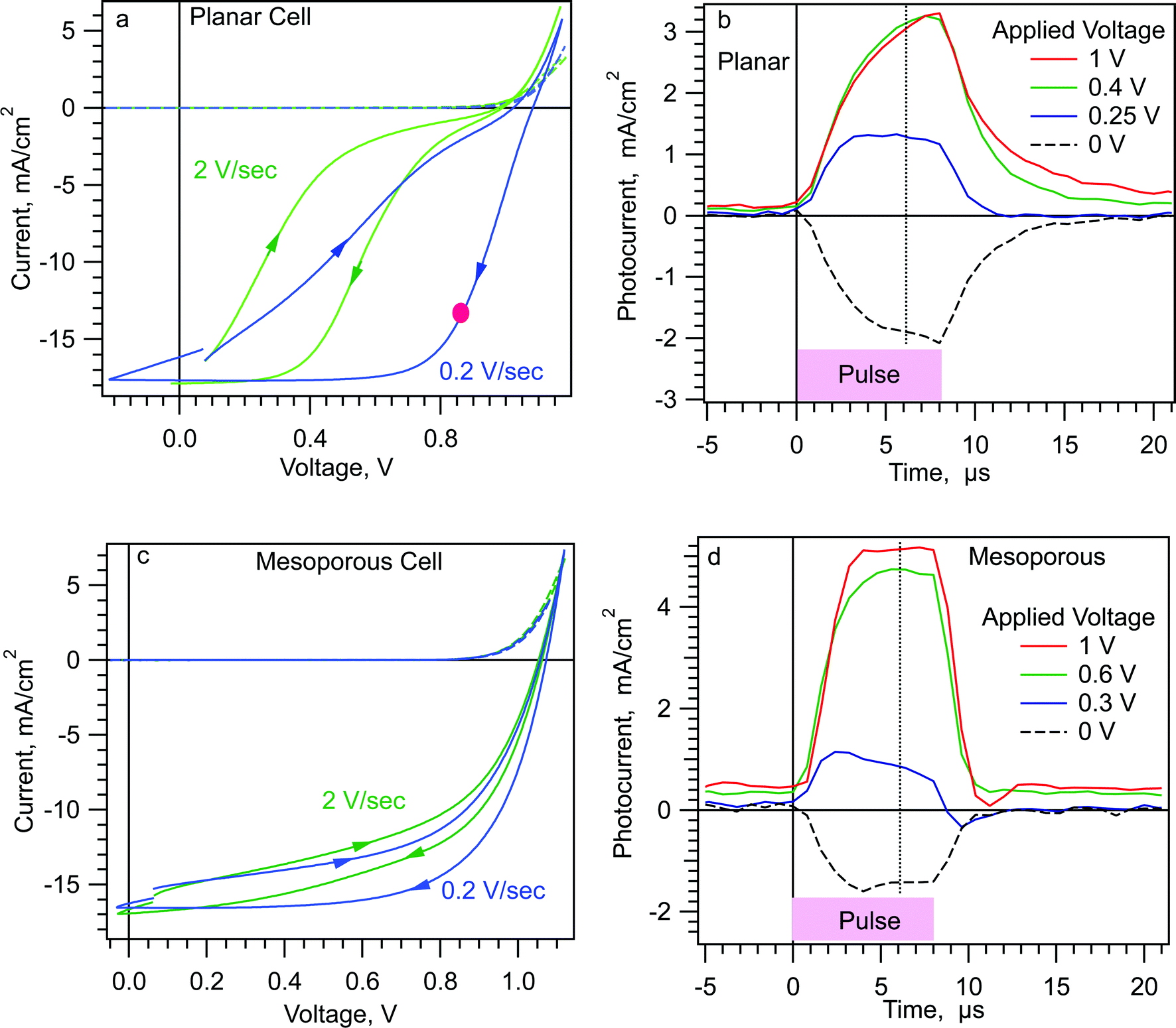 | ||
| Fig. 1 (a and c) JVs of planar and mesoporous MAPI cells at 1 Sun and dark. The red dot is the stabilized current at a fixed voltage of 0.85 V. (b and d) Photocurrent transients from the Step-Dwell-Probe (SDP) experiment at short circuit (0 V) and various forward bias voltages. Pulse was 8 μs long, from a 735 nm LED. Cells equilibrated for ≥1 minute at dark short circuit between SDP experiments. Although the photocurrent in (b) did not reach a plateau during the 8 μs pulse, longer pulse data shows the plateau occurs by ∼12 μs with only 5% higher current (Fig. S3a, ESI†). | ||
In Fig. 1b we show the photocurrent transients at various forward bias voltages for the same cell. The transients were taken 100 μs after the voltage step to forward bias (see Scheme 2a). The pulse light source was a 735 nm LED and the pulse length was 8 μs. At short circuit (black) the photocurrent transient is negative, with a peak of −2 mA cm−2. At an applied forward bias of 0.25 V the photocurrent transient is positive, with a magnitude of 1 mA cm−2. At ≥0.4 V, the transient photocurrent reaches +3 mA cm−2, larger in magnitude than the negative transient at short circuit. Fig. 1c shows JVs for a FTO/c-TiO2/m-TiO2/MAPI/Spiro/Gold cell. This cell shows significantly less JV hysteresis than the planar cell in Fig. 1a and b. Fig. 1d shows the photocurrent transients measured as in Fig. 1b. Again, at ≥0.3 V forward bias the photocurrent transients are positive, and at ≥0.6 V they are significantly larger in magnitude than the short circuit photocurrent transient. (We note that the rise and fall of the photocurrent transients in our cells is RC limited. The slower rise and fall for the planar cell results mainly from a larger series resistance for this particular cell.)
Fig. 2 shows a summary of the data from the experiments shown in Fig. 1b and d. In Fig. 2 we have plotted the transient photocurrent at 6 μs into the pulse (dotted line in Fig. 1b and d) vs. the applied voltage. Hereafter we will refer to the complete photocurrent transient as the “Jtr” and the current at a particular time “t” after the start of the pulse as Jtr-t, e.g. Jtr-6μs. The data in Fig. 2 are representative of the four planar TiO2/MAPI cells, three mesoporous TiO2/MAPI cells, and one MAPbBr cell that we have tested. We have recently shown that some “top cathode” MAPI cells with PEDOT and PCBM contact layers also show positive photocurrent transients after a step to forward bias.31 The similarity between the m-TiO2 and planar cell in Fig. 2 might seem unusual given the large difference in the hysteresis shown in Fig. 1. However, because of the short dwell time, the data in Fig. 2 reflect the state of the cell at SC in the dark, whereas the JV hysteresis is a result of how that state evolves at longer times under applied bias.
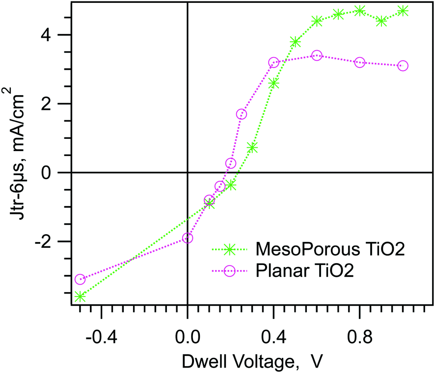 | ||
| Fig. 2 Results for the SDP experiment on two MAPI cells. Jtr-6μs after a dwell time of 100 μs vs. dwell voltage. | ||
Fig. 1 and 2 confirm the wiggly band model shown in Scheme 1. The positive photocurrent transients at 0.3 V forward bias, which is quite small compared to Vbi, are exactly as predicted from Scheme 1c and d. The fact that it requires ≤0.3 V forward bias to create a positive Jtr, implies that region II in Scheme 1c occupies most of the MAPI thickness. In other words the mobile ion screening of the built-in field at SC results in thin space charge layers. (We note again that we are using “mobile ion” as shorthand for all types of polarizable charged defects and dipoles.)
Estimation of the space charge layer thickness
The magnitude and sign of the photocurrent transients can be used to infer information about the width of region II. A salient feature of Fig. 2 is the plateau of Jtr-6μs between ∼0.5 and 1 V. The plateau can be explained as follows. The plateau begins at the applied potential where collection of the photocurrent across region II reaches a maximum possible internal quantum efficiency. At higher potentials, the larger slope of the potential across region II does not significantly increase the photocurrent collection across region II, or decrease it across regions I and III, therefore the Jtr-6μs remains essentially constant. The measured photocurrent in the plateau is still the sum of the photocurrents from regions I, II, and III. We can use this fact to estimate the fraction of the total absorber thickness (Wa) taken up by region II (WII/Wa), at a given applied voltage, using eqn (1).| WII/Wa ≥ (Jtr-max − Jtr-p)/(2Jtr-max) | (1) |
We digress here briefly to discuss the similarity in the width of region II in both kinds of cells. The mesoporous TiO2 layer is approximately 250 nm thick, thus occupying about 2/3 of the MAPI layer thickness. Thus for a WII occupying 90% of the cell, most of the m-TiO2/MAPI layer lies inside region II. This implies the following picture of the cell. At short circuit, ions are able to move in the MAPI inside the m-TiO2 as well as in the capping layer. The moving ions screen the built-in field down to the last part of the m-TiO2/MAPI layer near the compact TiO2 underlayer. Because the m-TiO2 is close to intrinsic, there are too few free electrons or holes to have any effect on the field distribution. Thus there is also no field in the TiO2 except in the bottom ≤17 nm. The space charge layer thickness in the m-TiO2 film is controlled by the characteristics of the MAPI, however the high surface area of m-TiO2 layer could have an indirect effect on the concentration and/or mobility of the mobile ions in the MAPI.
Just after the m-TiO2 cell is placed in forward bias, the situation in both types of cells resembles that drawn in Scheme 1c and d. One important difference is that in the m-TiO2/MAPI cell photoexcited electrons may transfer to the m-TiO2. However, in region II electrons in the m-TiO2 will drift away from the c-TiO2 contact, just as they do in the MAPI in the planar cell. The electrons may not be able to reach the MAPI conduction band valley near the Spiro, but the difference in the resulting displacement current will not be large when the capping layer is thin. For this reason the results in Fig. 1 and 2 are similar for both types of cells. More detailed measurements with differing capping layers may be able to distinguish between the two types of cells.
Timescale for relaxation of the field screening
We now discuss the relaxation of the mobile ions to a new equilibrium after a step from SC to fixed forward bias. If the cell is held at a given forward bias (Vd) for some dwell time (td) the mobile ions will migrate back along the potential gradient in region II (Scheme 3a and b). As the charges move, they will reduce the “reverse” potential difference across region II. As the potential difference in region II decreases, the short pulse Jtr (as in Fig. 1) should become less positive. The Jtr-6μs will have a magnitude of zero when the positive contribution from region II equals the negative contribution from regions I and III. With more time at forward bias, the mobile ions will reach a new equilibrium and the potential across region II will become flat. If the applied potential is significantly less than Vbi, then the photocurrent transient should become negative (Scheme 3b). We examine this prediction with the data in Fig. 3.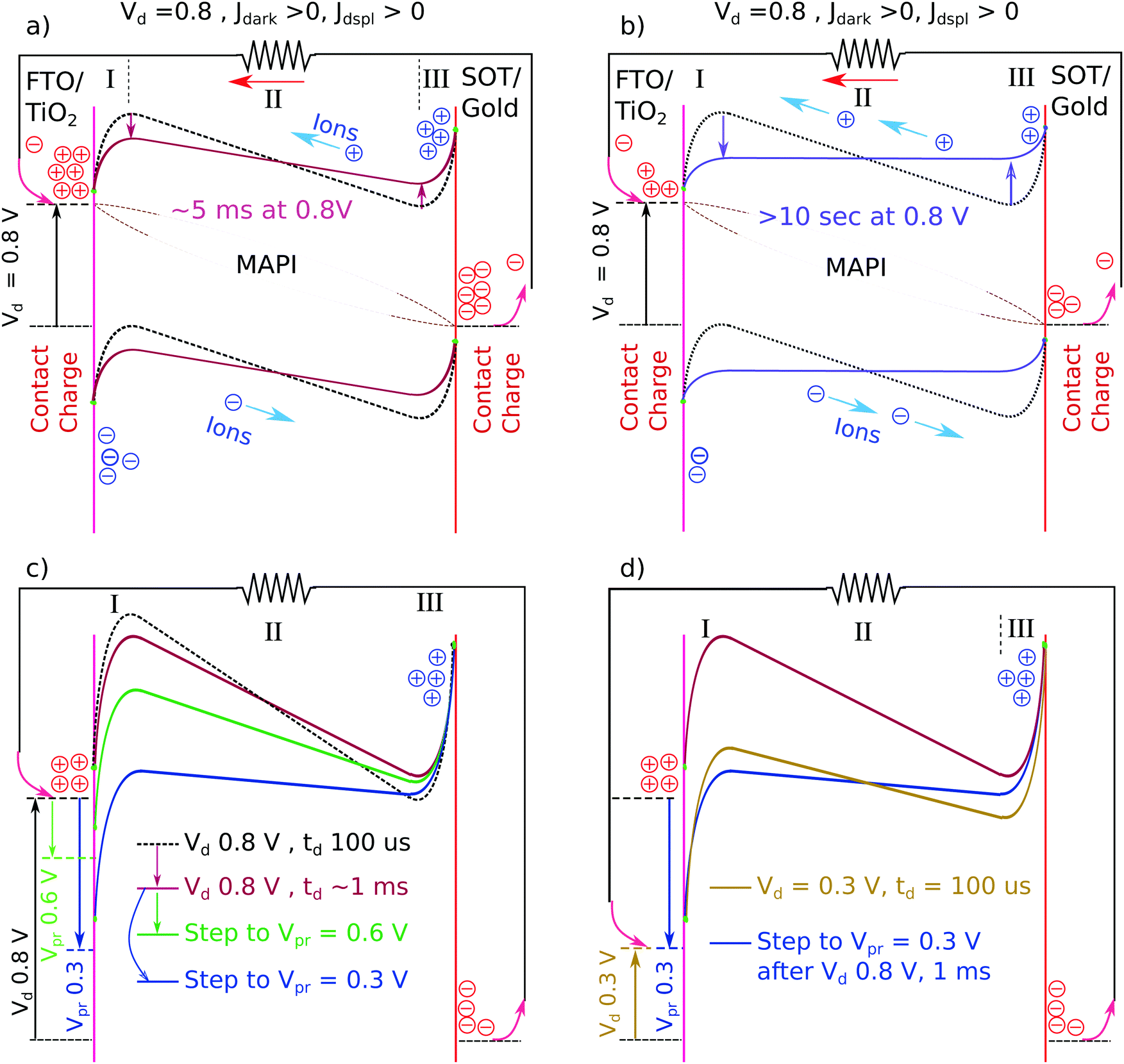 | ||
| Scheme 3 (a and b) Hypothesized evolution of the band energy profiles under forward bias due to the re-equilibration of mobile ions. Jdark and Jdisp as in Scheme 1. (c and d) Band energy profiles in the Step-Dwell-Step-Probe (SDSP) experiment. Only conduction band shown, vertical scale double that of panel a and b. (c) Showing the hypothesized change in band energy profile after ∼1 ms at 0.8 V and then the further change caused by a step to Vpr = 0.6 or 0.3 V. (d) Comparison of the band energy profiles after a step from 0 V to 0.3 V, and after a step back to 0.3 V after ∼1 ms at 0.8 V. | ||
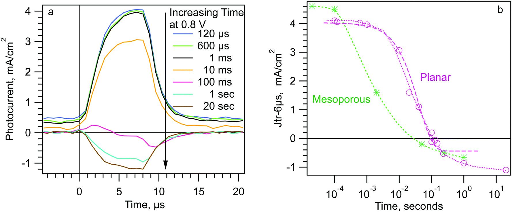 | ||
| Fig. 3 (a) Photocurrent transients from the SDP experiment for a dwell voltage of 0.8 V and various dwell times. (b) Jtr-6μs vs. dwell time at dwell voltage 0.8 V for the planar and mesoporous cells used in Fig. 1 and 2. | ||
Fig. 3a shows a series of photocurrent transients taken after different dwell times (td) at 0.8 V for a planar TiO2/MAPI/Spiro cell. The sequence of the “step dwell probe” (SDP) experiment is shown in Scheme 2a. No significant change is apparent until td ≳ 2 ms. At td = 10 ms, the transient is noticeably less positive, implying that the size of, or collection efficiency in, region II has decreased. At 100 ms, the Jtr is approximately zero. At td > 1 second at 0.8 V the transient becomes negative. Fig. 3b shows the evolution of the Jtr-6μs with td on a log time axis for a planar and a mesoporous cell. For the planar cell the evolution occurs over the time from 2 ms to >20 seconds. (We treat the apparent difference in response rate between the m-TiO2 and planar cells in the next section.) The purple long-dashed line in Fig. 3b is a single exponential fit to the data. The early part of the evolution can be fit by an exponential with a time constant of ∼40 ms, but the entire evolution cannot be fit by a single exponential. The later part of the evolution (1–20 seconds) occurs much more slowly. Many other cells, but not all, show this two part evolution (Fig. S4, ESI†). We note that the fastest changes in Jtr-6μs (e.g. <10 ms) could be due to ion movement or to trapping of electronic charges injected into the MAPI layer by the applied bias. In other words, electrons injected over the conduction band peak (at the region I/II boundary) and/or holes injected over the valence band “peak” at the region II/III boundary. We give some arguments concerning these two possibilities in the ESI,† however, our data cannot distinguish between them at this point. For the rest of the results section we retain the usage “mobile ions” for simplicity.
To determine the uniqueness of these transients, we have also tested the SDP experiment on silicon cells, dye sensitized cells, and polymer/PCBM cells. None of these cell types show positive photocurrent transients at forward bias voltages less than Vbi (Fig. S5, ESI†). At potentials larger than Vbi, polymer cells show a constant positive photocurrent transient, as expected (Fig. S5c, ESI†). We have also tested a single CdTe cell. For this cell, we do measure small positive photocurrent transients for voltages very near Voc, and for very short dwell times (Fig. S6, ESI†) The time scales for the evolution of the positive transients in CdTe are so different from those we observe for MAPI (Fig. 3) that we cannot yet say whether or not they stem from the same physical mechanism. Additional measurements on CdTe, and CIGS cells will be required.
Measurement of screening relaxation at short times
The SDP experiment turns out to be insensitive to the initial changes in charge screening at short dwell times. This is due to the plateau in Jtr-6μs at higher voltages visible in Fig. 2. In Fig. 2, where td = 100 μs for all points, the planar cell gives the same Jtr-6μs for voltages between 0.4 and 1 V. As mentioned before, this is because the collection efficiency from region II into the band valleys is already at maximum at Vd = 0.4 V and does not change between Vd = 0.4 V and 1 V. To see the effect of this plateau on the data in Fig. 3, consider a planar cell biased at 0.8 V for some time ≤2 ms. The mobile ions will move to decrease the field across region II (VII). At some time, VII will have decreased from 0.64 to 0.45 V. (Recall that, for the planar cell, VII is about 80% of Vd.) This is a significant change in VII, however we will not see any change in the Jtr-6μs measurement because the collection efficiency across region II has not yet decreased. We will not see any significant change in the Jtr-6μs until VII has decreased to ≤0.3 V. This change apparently takes >2 ms at 0.8 V. Consistent with this, increasing the applied voltage increases the dwell time before a change is observed in the Jtr-6μs (Fig. S4, ESI†). Another manifestation of this effect is shown by the mesoporous cell in Fig. 3b. In Fig. 2, the plateau of Jtr-6μs for the mesoporous cell starts at 0.6 V, closer to 0.8 V than for the planar cell. Consequently, less decrease of VII is required in the mesoporous cell before an effect is seen on Jtr-6μs. Consistent with this, Jtr-6μs of the mesoporous cell begins to decrease at td = ∼200 μs in Fig. 3b.In order to correctly measure the evolution of the band energy profile at very short times we have developed a new experiment that uses two voltage steps. A schematic of the experiment is shown in Scheme 2b and the associated band edge profiles are shown in Scheme 3. We refer to this experiment as Step-Dwell-Step-Probe (SDSP). First, we let the mobile ion distribution evolve at Vd, for a time td. Then we shift to a different voltage, V probe (Vpr), where we measure a Jtr after 40 μs. The 40 μs dwell is to allow the electrode capacitance to discharge. The rational of the experiment is as follows (Scheme 3c). By stepping from a given Vd to a lower Vpr we can quickly decrease the value of VII by a fixed amount, whatever the value of VII was before the step. With a very short dwell at Vpr, no further motion of the mobile ions will occur before the transient is measured. Thus, after a short (e.g. 1 ms) dwell at Vd, and then stepping to the correct Vpr, we can shift VII from a value in the plateau region of Fig. 2, to a value below the plateau region where Jtr-6μs will be effected by the change in the mobile ion distribution that happened at Vd. Scheme 3c shows the theory for the specific example of Vd = 0.8 V, td = ∼1 ms, and Vpr = 0.6 or 0.3 V and Fig. 4a shows the measured Jtrs. In Fig. 4a, the step to Vpr = 0.6 causes only a small change in the Jtr relative to Vpr = 0.8 V. However, the step to Vpr = 0.3 decreases VII from 0.45 V, where Jtr-6μs is in the plateau region, to 0.075 V, where the Jtr-6μs will be negative (solid blue line in Fig. 4a). By contrast, applying Vd = 0.3 V for only 100 μs (as in Fig. 2) results in a positive transient (Scheme 3d).
 | ||
| Fig. 4 Results of SDSP experiments on a planar MAPI cell. (a) Example photocurrent transients for a dwell voltage (Vd) of 0.8 V. (b) Jtr-6μs vs. Vpr and td, from SDSP experiments using a dwell voltage of 0.8 V. | ||
Fig. 4b shows the resulting Jtr-6μs for Vd = 0.8 V and a wide range of td and Vpr. To perform the experiment, we use one Vd, and a given td, and then measure Jtr-6μs across the range of Vpr. We then change td and again scan across Vpr. Between each Jtr acquisition, the cell is allowed to relax for 1 minute or more at short circuit in the dark. The cell for Fig. 4 was a planar TiO2/MAPI/Spiro device from the same batch as the ones shown in Fig. 1–3. The dwell times range from 100 μs to 150 ms, and the probe voltages from −0.8 V (reverse bias) to 1.1 V, just beyond the steady state Voc. The points of a given dwell time are connected by dotted lines. A selection of the photocurrent transients is shown in Fig. S7 (ESI†). The red circles show the Jtr-6μs at various Vpr after a dwell of 100 μs at 0.8 V. The blue squares are Jtr-6μs at Vpr after a 1 ms dwell at 0.8 V. Although there is no change to the transient at Vpr = 0.8 V, there is a significant shift toward the negative in the transients with Vpr ≤ 0.5 V (blue arrow in Fig. 4 and data in Fig. S8, ESI†). Between 0 and 0.5 V, the td = 1 ms data are shifted about 0.1 V to the right of the td = 100 μs data. The green triangles are the Jtr-6μs at Vpr after a 5 ms dwell at 0.8 V. Again, the transient at Vpr = 0.8 V hardly changes at all, however, there is a large change in the transient at Vpr = 0.5 V. Between Vpr = 0 to 0.7 V the green points are shifted about 0.4 V to the right of the red points (green arrow). From this we can conclude that during 1 ms at 0.8 V, the mobile ions move enough to remove 0.08 V of the original potential difference across region II (V0II). Likewise, during 5 ms at 0.8 V, the mobile ions move enough to remove 0.32 V of V0II. (Recall that the change in VII is ∼80% of the change in applied voltage (Vpr–Vd), see Scheme 1.)
An interesting feature of Fig. 4 is that the lines of Jtr-6μs vs. Vpr are nearly parallel. The simplest way to explain this result is that the thickness of regions I and III, the space charge layer width, does not change as the mobile ions equilibrate to the new potential, at least out to 150 ms. This is consistent with the behavior of an electrolyte, where the Debye length is a function of the ion concentration, but essentially independent of the potential drop. In contrast, the depletion width of a Schottky barrier or n–p junction, determined by fixed donors and free charges, changes significantly with applied potential. This is a significant difference in operation between MAPI cells and conventional inorganic solar cells that highlights the need for care in applying conventional analytical methods.
Verification of wiggly band model with two pulse wavelengths
We have so far provided time-dependent evidence for the wiggly band model in Scheme 1. However, we can also test the model using probe pulses of different colors. According to the model, a pulse that is more strongly absorbed in region I (e.g. a blue pulse) should cause a larger negative Jtr contribution from region I and a smaller positive contribution from region II. The Jtr from the blue pulse should therefore be more negative than that created by a less strongly absorbed pulse (e.g. 735 nm). We can measure this effect most easily where one of the pulse colors gives a Jtr that is near zero in magnitude. Fig. 5 compares NIR and blue pulse Jtrs for a m-TiO2/MAPI cell with Vd = 0.3 V and td = 2 ms. At this dwell voltage and time the Jtr-6μs for a NIR pulse is essentially zero. This means that for the NIR pulse, the photocurrent contributions of the three regions are balanced. Under the same conditions the Jtr-6μs for a blue pulse is negative due to the stronger absorption in region I, confirming the model. Fig. S9 (ESI†) shows that at the Vd and td where the blue pulse Jtr is near zero, the NIR Jtr is positive. Comparing different color pulses when one color gives a Jtr near zero has the advantage that the pulses do not need to have the same number of absorbed photons in order to observe the sign of the Jtr from the second color pulse. However, it does have the disadvantage that small magnitude Jtrs have low signal to noise. Despite the noise, the data clearly show the predicted effect. With a good optical model, and a range of pulse colors, one could in principle use the color dependence of the Jtrs to estimate the space charge layer width in the MAPI.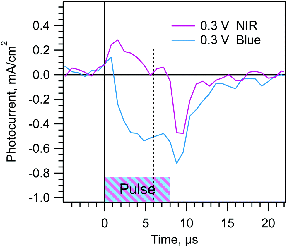 | ||
| Fig. 5 Effect of blue vs. NIR (735 nm) pulses at Vd and td where the photocurrents from regions I and III vs. region II are balanced for the NIR pulse. The peaks at 1 μs and 9 μs are from the switching of the LED. Data from a m-TiO2/MAPI cell with td = 2 ms and Vd = 0.3 V. | ||
Discussion
We believe the data in Fig. 1–5 provide very solid evidence for the previously hypothesized existence of a significant field free zone (region II) across the center of the MAPI layer at short circuit. The field free zone is created by mobile ions (again, we use the term to include all mobile charged atoms, defects, and dipoles). The field screening exhibits a range of response times (ms to s) to changes in applied potential. The slower response times contribute a large part of the JV hysteresis that is observed in these cells. In the rest of this section we discuss some anomalous features of the response of MAPI cells to longer light pulses at forward bias. We have placed this material in the discussion section because, although we think the data are important, we are not able to give a conclusive interpretation. The more speculative nature of the discussion below should not detract from the solid conclusions mentioned just above.Anomalous behavior of long pulse photocurrent transients
Fig. 6a shows the photocurrent transient from a 1 ms pulse at both short circuit (black) and 0.5 V forward bias (blue). At short circuit, the photocurrent transient is negative and constant during the pulse. The photocurrent transient at 0.5 V is positive and decreases to zero in ∼1 ms. A decreasing positive photocurrent with time is the expected behavior from Scheme 1d. This is because photogenerated charge cannot collect indefinitely in the band valleys. Increasing charge density in the band valleys will increase recombination until an equilibrium charge density is reached, at which point the displacement current in the external circuit will be zero. However, as usual in perovskite solar cells, the actual situation is not so simple. The green curve in Fig. 6a shows the photocurrent transients at 0.5 V generated by a series of 100 μs NIR (735 nm) pulses separated by 200 μs dark. A striking feature of the green curve is that the initial photocurrent from each of the latter pulses is nearly identical to the photocurrent at the end of the previous pulse. (See the horizontal green dotted line in the figure.) A similar experiment with a 1 ms dark interval shows the same pattern, Fig. 6b. This pattern indicates that the physical state of the cell when the light is turned off has not changed when the light is turned back on. We will refer to this as an optical memory effect. Fig. S10 and S11 (ESI†) illustrate that a 1 ms light pulse can generate an optical memory that lasts up to one second. Another important feature of the multi-pulse transients in Fig. 6 is that the dark current directly after the light is turned off shows only a small overshoot towards the negative (e.g.Fig. 6a at 0.4 ms and Fig. 6b at 1.1 ms).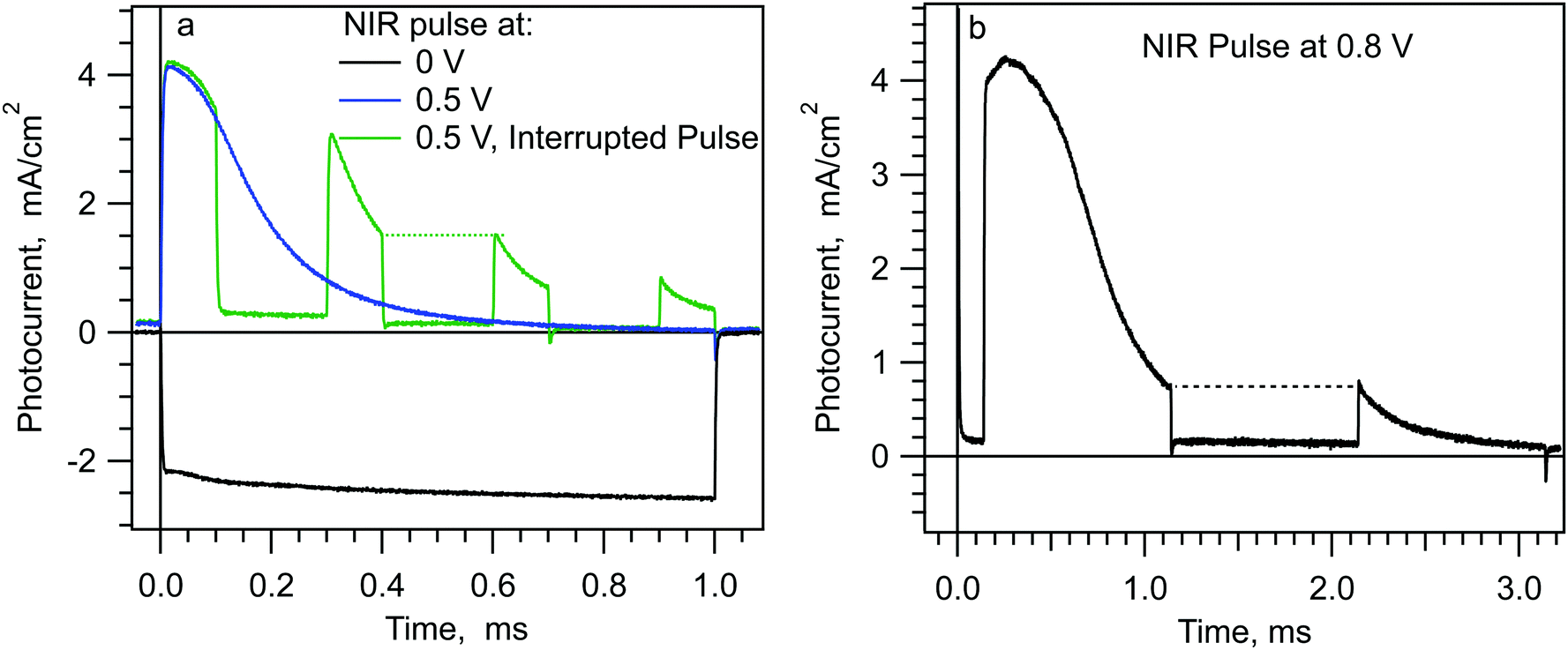 | ||
| Fig. 6 Photocurrent transients from longer light pulses. Transients from the same planar cell shown in Fig. 1 and 2. Pulses from a 735 nm LED. | ||
The lack of overshoots at both light on and light off has strong implications regarding the nature of the charge collection in the band valleys. Specifically, it indicates that there is very little free charge (i.e. un-trapped electrons and holes) in the cell at any point during the photocurrent transient at forward bias. To understand this assertion, consider the situation at 0.4 ms along the green curve, just before the light is turned off. At that point, the photocurrent has decreased from 4 mA cm−2 to 1.5 mA cm−2. Assuming that light absorption and charge separation have not changed during the first 0.4 ms, this means that 2.5 mA cm−2 of recombination is occurring in the cell. Integrating the photocurrent from 0 to 0.4 ms, and assuming mainly displacement current, we find ∼0.6 μC will have collected in the band valleys. Just after the light is turned off, recombination will begin to drain the accumulated charge in the band valleys, resulting in a negative displacement current in the external circuit. The recombination current would continue as long as there was accumulated free charge to recombine. Thus, if any significant part of the accumulated charge were able to recombine, the initial negative displacement current would equal the recombination current (−2.5 mA cm−2) and decay over tens of μs. Instead, we measure ∼60 μA cm−2 of negative displacement current after the light is turned off at 0.4 ms. From this, we conclude that there is very little free charge present at 0.4 ms. The negative overshoot does increase for subsequent light off steps, e.g. 0.7 ms, but it never becomes larger than 0.35 mA cm−2.
Possible mechanisms for the long pulse transients
There are two possible explanations for the lack of free charge in the band valleys. Either the photocurrent generated by the light pulse is all flowing into deep charge traps in the band valleys, or a significant amount of the photo-excited charge is actually flowing out of the band valleys by transfer to the adjacent electrode. The latter possibility implies that after equilibration at dark SC and a step to forward bias, the hole and/or electron collecting electrode(s) must be non-selective (i.e. “leaky”). Our current data does not distinguish between the two explanations, but in order to encourage future research, we discuss briefly the implications of each. The implications developed appear to be testable.First, if all of the photogenerated charges are flowing into deep traps, we can estimate the number of traps required. The integrated positive current in Fig. 6b is about 3 μC cm−2. Assuming the trapped electrons (and/or holes) are situated in a layer of ∼50 nm thickness, the trap density would have to be ≥4 × 1018 cm−3. This value is high, but might be possible. In addition, however, these trapped electrons must have lifetimes of ≥10 ms for there to be so little decay in their population over 1 ms (Fig. 6b). This lifetime seems anomalously long. Traps normally accelerate recombination, thus the lifetime of trapped charges is normally short. We have performed additional experiments in an attempt to measure the lifetime of the effect of a pulse of light on the cell (Fig. S10 and S11, ESI†). Fig. S11 (ESI†) presents an experiment wherein we first expose the cell to 1 ms of 1 Sun at SC, delay up to 1 second in the dark at SC, and then perform a SDP experiment at 0.8 V. In this cell, about one half of the effect of a 1 ms pulse of light is still present after one second. This long lifetime appears to argue against electrostatic trapping of charges as the explanation for Fig. 6. Chemical trapping, in other words charge localization accompanied by the rearrangement of atoms or bonds, would seem to be required. In addition to the long lifetime, the charge traps must be inhomogeneously distributed across the cell. Electrons and holes trapped homogeneously in space do not contribute to a change in electric field, thus give no displacement current. The traps could be related to the ion vacancies or interstitials created during the equilibration to the built-in field, but we have no proof for this association.
We now examine the other possibility; that the lack of free charges in the band valleys is due to leakage of charges from the band valleys to the adjacent “wrong” electrodes. Poor selectivity at the electrodes (a.k.a. surface recombination) has been previously invoked as necessary for the JV hysteresis, and the characteristics of photovoltage transients.13,31 If the leakage current is high very little charge accumulates in the band valleys and the lack of overshoot at the light turn-off is expected. However if there are few charges in the band valleys, the decrease in photocurrent over the first 1 ms cannot be due to a change in the potential profile. Instead, we have to explain the decreasing photocurrent by a rapid decrease in the leakage current. In other words, by a rapid increase in the selectivity of the electrode(s). Whatever physical change causes the decreasing photocurrent must also be consistent with the memory effect. We can most easily explain the decreasing current and the memory effect if the increase in electrode selectivity is caused by ion motion. Ions that have drifted to or away from the surface during the light pulse will not drift back in the dark because the voltage bias is still applied. In Fig. 6, one ms of NIR illumination at 0.8 V reduces the subsequent photocurrent peak from 4 to 0.7 mA cm−2. However, the same decrease in the photocurrent peak with time also occurs under dark bias, only much more slowly. From Fig. 3b we can see that for the planar cell it takes about 50 ms at 0.8 V for the Jtr-6μs to decrease from 4 to ∼0.7 mA cm−2. Thus, for the same bias voltage, the decrease in the photocurrent transient magnitude occurs ∼50 times faster under light than in dark.
In summary, if we reject the “long lived trapping without recombination” explanation discussed above, we are forced to assert that light can have a large effect on the mobile ion mobility, concentration, or impact on the electrodes. As with the long lived trapping, we do not have a physical explanation for this phenomena. However, possible effects of light absorption on the structure of MAPI have been observed by other authors. Zhou et al. measured a significant expansion of the MAPI lattice (up to 0.1%) under illumination.45 They theorized that photogenerated charges reduce the barriers to methylammonium (MA) rotation. Similarly Coll et al. measured a 4 fold increase in the piezoelectric coefficient under illumination.46 Liu et al. developed a possible model for this photo-piezoelectric effect, again based on reduction of the barrier for MA rotation.47 Although we do not endorse any particular explanation at this time, the proposed photo-induced acceleration of MA rotation could probably explain our observations.
Lastly, we point out that the above analysis has been carried out in the context of a one dimensional model. Some of the results in Fig. S10 and S11 (ESI†) may need to be explained by lateral variation of cell characteristics. For example, dark injected charges will follow paths of least resistance across the cell. It could be the case that the dark current flows through only a small fraction of the absorber layer volume. In such a case, the distribution of the applied potential in the MAPI will also differ laterally. Where the bulk resistance is low, surface resistance will dominate and the applied field will drop at the surface. Where MAPI resistance is high, the field will drop across the bulk of the absorber, causing more ion movement across region II. On the other hand, during a light pulse, photogenerated charges are created more or less homogeneously. If the trapping and recombination are distributed unevenly in the lateral dimensions, as well as in the vertical, dark injected and photogenerated charges could end up in different traps.
We have examined the anomalous characteristics of the long and interrupted photocurrent transients in Fig. 6. The first level implication is clear; there is no significant free charge accumulating in the band valleys during a long light pulse on this cell, yet the photocurrent decreases quickly. We have proposed two possible explanations, each of which require a novel physical phenomena to be occurring. We hope to confirm one or the other of these hypotheses in the near future.
Conclusions
Measurement of photocurrent transients under applied bias is a simple technique that can be used to investigate many of the unusual characteristics of MAPI solar cells. The technique is inexpensive, fast, and non-destructive. With these initial measurements we have shown that the proposed “wiggly band” model of mobile ion field screening and hysteresis is correct. We have also shown that the field screening by the mobile ions behaves as expected for an electrolyte, e.g. the space charge layer width (Debye length) does not change significantly as a function of bias. Analysis of long pulse and interrupted pulse transients at forward bias shows that simple ion movement alone cannot explain all the observed phenomena. We are led to propose either large concentrations of very long lived trapped charges, or a photo effect on the characteristics of the mobile ions. We expect further use of the techniques described above, especially with the addition of temperature dependence, will allow us to untangle this issue and provide additional insights into electronic and ionic processes in perovskite solar cells.Acknowledgements
This work was supported by the Department of Energy Sunshot NextGen III program (Award Number DEEE0006707) and the UK Engineering and Physical Sciences Research Council (grants EP/J002305/1, EP/M023532/1, EP/I019278/1, EP/M025020/1, EP/G037515/1 and EP/M014797/1).References
- A. Kojima, K. Teshima, Y. Shirai and T. Miyasaka, J. Am. Chem. Soc., 2009, 131, 6050 CrossRef CAS PubMed.
- J. H. Im, C. R. Lee, J. W. Lee, S. W. Park and N. G. Park, Nanoscale, 2011, 3, 4088 RSC.
- X. Li, D. Q. Bi, C. Y. Yi, J. D. Decoppet, J. S. Luo, S. M. Zakeeruddin, A. Hagfeldt and M. Gratzel, Science, 2016, 353, 58 CrossRef CAS PubMed.
- W. S. Yang, J. H. Noh, N. J. Jeon, Y. C. Kim, S. Ryu, J. Seo and S. I. Seok, Science, 2015, 348, 1234 CrossRef CAS PubMed.
- W. J. Yin, T. T. Shi and Y. F. Yan, Appl. Phys. Lett., 2014, 104, 063903 CrossRef.
- R. Gottesman, E. Haltzi, L. Gouda, S. Tirosh, Y. Bouhadana, A. Zaban, E. Mosconi and F. de Angelis, J. Phys. Chem. Lett., 2014, 5, 2662 CrossRef CAS PubMed.
- C. Eames, J. M. Frost, P. R. F. Barnes, B. C. O'Regan, A. Walsh and M. S. Islam, Nat. Commun., 2015, 6, 7497 CrossRef CAS PubMed.
- A. M. A. Leguy, J. M. Frost, A. P. McMahon, V. G. Sakai, W. Kochelmann, C. H. Law, X. E. Li, F. Foglia, A. Walsh, B. C. O'Regan, J. Nelson, J. T. Cabral and P. R. F. Barnes, Nat. Commun., 2015, 6, 7124 CrossRef PubMed.
- H. J. Snaith, A. Abate, J. M. Ball, G. E. Eperon, T. Leijtens, N. K. Noel, S. D. Stranks, J. T. W. Wang, K. Wojciechowski and W. Zhang, J. Phys. Chem. Lett., 2014, 5, 1511 CrossRef CAS PubMed.
- E. L. Unger, E. T. Hoke, C. D. Bailie, W. H. Nguyen, A. R. Bowring, T. Heumüller, M. G. Christoforo and M. D. McGehee, Energy Environ. Sci., 2014, 7, 3690 CAS.
- W. Tress, N. Marinova, T. Moehl, S. M. Zakeeruddin, M. K. Nazeeruddin and M. Gratzel, Energy Environ. Sci., 2015, 8, 995 CAS.
- Y. B. Yuan and J. S. Huang, Acc. Chem. Res., 2016, 49, 286 CrossRef CAS PubMed.
- S. van Reenen, M. Kemerink and H. J. Snaith, J. Phys. Chem. Lett., 2015, 6, 3808 CrossRef CAS PubMed.
- K. Wojciechowski, S. D. Stranks, A. Abate, G. Sadoughi, A. Sadhanala, N. Kopidakis, G. Rumbles, C.-Z. Li, R. H. Friend, A. K.-Y. Jen and H. J. Snaith, ACS Nano, 2014, 8, 12701 CrossRef CAS PubMed.
- P. W. Liang, C. C. Chueh, S. T. Williams and A. K. Y. Jen, Adv. Energy Mater., 2015, 5, 2321 Search PubMed.
- Y. H. Shao, Z. G. Xiao, C. Bi, Y. B. Yuan and J. S. Huang, Nat. Commun., 2014, 5, 5784 CrossRef CAS PubMed.
- D. Bryant, S. Wheeler, B. C. O'Regan, T. Watson, P. R. F. Barnes, D. Worsley and J. Durrant, J. Phys. Chem. Lett., 2015, 6, 3190 CrossRef CAS.
- M. De Bastiani, G. Dell'Erba, M. Gandini, V. D'Innocenzo, S. Neutzner, A. R. S. Kandada, G. Grancini, M. Binda, M. Prato, J. M. Ball, M. Caironi and A. Petrozza, Adv. Energy Mater., 2016, 6, 1501453 CrossRef.
- W. Chen, Y. Z. Wu, Y. F. Yue, J. Liu, W. J. Zhang, X. D. Yang, H. Chen, E. B. Bi, I. Ashraful, M. Gratzel and L. Y. Han, Science, 2015, 350, 944 CrossRef CAS PubMed.
- Z. Xiao, Y. Yuan, Y. Shao, C. Wang, Q. Dong, B. Cheng, P. Shamar, A. Gruverman and J. Huang, Nat. Mater., 2015, 14, 193 CrossRef CAS PubMed.
- V. W. Bergmann, Y. Guo, H. Tanaka, I. M. Hermes, D. Li, A. Klasen, S. A. Bretschneider, E. Nakamura, R. Berger and S. A. L. Weber, ACS Appl. Mater. Interfaces, 2016, 8, 19402 Search PubMed.
- D. W. Dequilettes, W. Zhang, V. M. Burlakov, D. J. Graham, T. Leijtens, A. Osherov, V. Bulovic, H. J. Snaith, D. S. Ginger and S. D. Stranks, Nat. Commun., 2016, 7, 11683 CrossRef CAS PubMed.
- H. Yu, H. P. Lu, F. Y. Xie, S. Zhou and N. Zhao, Adv. Funct. Mater., 2016, 26, 1411 CrossRef CAS.
- C. Li, S. Tscheuschner, F. Paulus, P. E. Hopkinson, J. Kiessling, A. Kohler, Y. Vaynzof and S. Huettner, Adv. Mater., 2016, 28, 2446 CrossRef CAS PubMed.
- O. Almora, A. Guerrero and G. Garcia-Belmonte, Appl. Phys. Lett., 2016, 108, 043903 CrossRef.
- A. K. Jena, H.-W. Chen, A. Kogo, Y. Sanehira, M. Ikegami and T. Miyasaka, ACS Appl. Mater. Interfaces, 2015, 7, 9817 CAS.
- G. E. Eperon, G. M. Paterno, R. J. Sutton, A. Zampetti, A. A. Haghighirad, F. Cacialli and H. J. Snaith, J. Mater. Chem. A, 2015, 3, 19688 CAS.
- Y. Zhao, C. J. Liang, H. M. Zhang, D. Li, D. Tian, G. B. Li, X. P. Jing, W. G. Zhang, W. K. Xiao, Q. Liu, F. J. Zhang and Z. Q. He, Energy Environ. Sci., 2015, 8, 1256 CAS.
- Y. Zhang, M. Z. Liu, G. E. Eperon, T. C. Leijtens, D. McMeekin, M. Saliba, W. Zhang, M. de Bastiani, A. Petrozza, L. M. Herz, M. B. Johnston, H. Lin and H. J. Snaith, Mater. Horiz., 2015, 2, 315 RSC.
- T. Leijtens, A. R. S. Kandada, G. E. Eperon, G. Grancini, V. D'Innocenzo, J. M. Ball, S. D. Stranks, H. J. Snaith and A. Petrozza, J. Am. Chem. Soc., 2015, 137, 15451 CrossRef CAS PubMed.
- P. Calado, A. M. Telford, D. Bryant, X. Li, J. Nelson, B. C. O'Regan and P. R. F. Barnes, Nat. Commun., 2016 DOI:10.1038/ncomms13831 , available at http://https://arxiv.org/abs/1606.00818.
- W. E. Spear, J. Non-Cryst. Solids, 1969, 1, 197 CrossRef CAS.
- S. Draguta, S. Thakur, Y. V. Morozov, Y. X. Wang, J. S. Manser, P. V. Kamat and M. Kuno, J. Phys. Chem. Lett., 2016, 7, 715 CrossRef CAS PubMed.
- Y. Kutes, Y. Y. Zhou, J. L. Bosse, J. Steffes, N. P. Padture and B. D. Huey, Nano Lett., 2016, 16, 3434 CrossRef CAS PubMed.
- M. J. Simpson, B. Doughty, B. Yang, K. Xiao and Y. Z. Ma, J. Phys. Chem. Lett., 2015, 6, 3041 CrossRef CAS PubMed.
- Y. B. Yuan, J. Chae, Y. C. Shao, Q. Wang, Z. G. Xiao, A. Centrone and J. S. Huang, Adv. Energy Mater., 2015, 5, 1500615 CrossRef.
- B. C. O'Regan, P. R. F. Barnes, X. E. Li, C. Law, E. Paomares and J. M. Marin-Beloqui, J. Am. Chem. Soc., 2015, 137, 5087 CrossRef PubMed.
- S. Meloni, T. Moehl, W. Tress, M. Franckevicius, M. Saliba, Y. H. Lee, P. Gao, M. K. Nazeeruddin, S. M. Zakeeruddin, U. Rothlisberger and M. Graetzel, Nat. Commun., 2016, 7, 10334 CrossRef CAS PubMed.
- G. Richardson, S. E. J. O'Kane, R. G. Niemann, T. A. Peltola, J. M. Foster, P. J. Cameron and A. B. Walker, Energy Environ. Sci., 2016, 9, 1476 CAS.
- J. J. Shi, X. Xu, H. Y. Zhang, Y. H. Luo, D. M. Li and Q. B. Meng, Appl. Phys. Lett., 2015, 107, 163901 CrossRef.
- W. H. Nguyen, C. D. Bailie, E. L. Unger and M. D. McGehee, J. Am. Chem. Soc., 2014, 136, 10996 CrossRef CAS PubMed.
- Y. Li, J. K. Cooper, R. Buonsanti, C. Giannini, Y. Liu, F. M. Toma and I. D. Sharp, J. Phys. Chem. Lett., 2015, 6, 493–499 CrossRef CAS PubMed.
- Plans for the TRACER hardware and software can be requested from the corresponding author.
- Viewing scheme 1, we reason that the space charge layer thickness we have determine is closer to the 1/(2e) decay length, whereas the Debye length is the 1/e length. Thus we use 1/2 of our space charge layer thickness as a very rough estimate of the Debye length.
- Y. Zhou, L. You, S. W. Wang, Z. L. Ku, H. J. Fan, D. Schmidt, A. Rusydi, L. Chang, L. Wang, P. Ren, L. F. Chen, G. L. Yuan, L. Chen and J. L. Wang, Nat. Commun., 2016, 7, 11193 CrossRef CAS PubMed.
- M. Coll, A. Gomez, E. Mas-Marza, O. Almora, G. Garcia-Belmonte, M. Campoy-Quiles and J. Bisquert, J. Phys. Chem. Lett., 2015, 6, 1408 CrossRef CAS PubMed.
- S. Liu, F. Zheng, I. Grinberg and A. M. Rappe, J. Phys. Chem. Lett., 2016, 7, 1460 CrossRef CAS PubMed.
Footnote |
| † Electronic supplementary information (ESI) available. See DOI: 10.1039/c6ee02914k |
| This journal is © The Royal Society of Chemistry 2017 |