
Skutterudite with graphene-modified grain-boundary complexion enhances zT enabling high-efficiency thermoelectric device†
Peng-an
Zong‡
ab,
Riley
Hanus‡
c,
Maxwell
Dylla
c,
Yunshan
Tang
a,
Jingcheng
Liao
a,
Qihao
Zhang
ab,
G. Jeffrey
Snyder
 *c and
Lidong
Chen
*ad
*c and
Lidong
Chen
*ad
aState Key Laboratory of High Performance Ceramics and Superfine Microstructures, Shanghai Institute of Ceramics, Chinese Academy of Sciences, Shanghai 200050, China. E-mail: cld@mail.sic.ac.cn
bUniversity of Chinese Academy of Sciences, Beijing 100049, China
cDepartment of Materials Science and Engineering, Northwestern University, Evanston, IL 60208, USA. E-mail: jeff.snyder@northwestern.edu
dShanghai Institute of Materials Genome, Shanghai 200444, China
First published on 4th November 2016
Abstract
Skutterudite materials are widely considered for thermoelectric waste heat recovery. While the skutterudite structure effectively scatters the high frequency phonons, grain-boundary engineering is needed to further reduce the thermal conductivity beyond simply decreasing grain size. Here, we show that reduced graphene oxide (rGO) increases the grain boundary thermal resistivity by a factor of 3 to 5 compared to grain boundaries without graphene. Wrapping even micron sized grains with graphene leads to such a significant reduction in the thermal conductivity that a high thermoelectric figure of merit zT = 1.5 was realized in n-type YbyCo4Sb12, while a zT of 1.06 was achieved in p-type CeyFe3CoSb12. A 16 leg thermoelectric module was made by using n- and p-type skutterudite–graphene nanocomposites that exhibited conversion efficiency 24% higher than a module made without graphene. Engineering grain boundary complexions with 2-D materials introduces a new strategy for advanced thermoelectric materials.
Broader contextWith the world population predicted to double by 2050, it is urgent to seek a variety of clean and renewable energy sources to meet the rapidly increasing demand for energy. Thermoelectrics is considered a promising alternative energy technology, effective at producing power locally from waste heat sources, such as automotive exhaust or industrial processes. The reduction of lattice thermal conductivity by grain boundary engineering, without deterioration of electron transport, is an effective strategy to increase thermoelectric efficiency. Grain boundaries contribute additional degrees of freedom for engineering polycrystalline materials, with grain boundary structure and composition becoming critically important when explaining electrical and thermal transport. We show here that not all grain boundaries are the same, not only can one engineer grain size but also orientation and coherency of the interfaces. Even more possibilities arise as one considers that the grain boundary region, or complexion, can also be modified with impurity atoms. Being only a single atomic layer, graphene (or another two-dimensional material) that coats or wraps grains can modify grain boundary complexions in ways fundamentally different than traditional grain boundary phases. This demonstration opens new possibilities for grain boundary engineering and understanding interfaces in thermoelectrics as well as other materials. |
Effective, reliable and clean energy conversion technologies are urgently sought after for energy harvesting. Thermoelectric materials, which can achieve direct heat-to-electricity conversion, have long been confined to use in space exploration, satellites, and other niche applications but are now being more widely considered for a large number of broad-based applications—such as the conversion of automotive exhaust heat to electricity.1–3 The conversion efficiency is determined by the dimensionless material figure of merit zT = (σS2/κ)T, where σ, S, κ and T are the electrical conductivity, Seebeck coefficient, thermal conductivity and absolute temperature, respectively. Recently, several novel approaches and strategies4–6 have been shown to effectively enhance zTs and numerous new TE materials7–9 have been reported. Among them, filled-skutterudites are one of the most promising material systems for TE power generation applications in the intermediate temperature range of ∼500–800 K.10,11 Filling the Sb-icosahedron cages with one or more atoms has been shown to be effective in controlling the charge carrier concentration and reducing lattice thermal conductivity κL, which enables high zTs.12–16
The incorporation of secondary phases into TE materials has been shown to improve thermoelectric performance in some cases.17,18 The improvements in zT cannot be explained by simply averaging the properties of the individual phases.19,20 Various interfacial mechanisms have been proposed to explain zT enhancement in these composite thermoelectrics. Carrier filtering effects and increased boundary scattering of low-frequency/long-wavelength phonons due to an increase in grain boundary interfacial area per volume have been cited as possible mechanisms.18
It has become increasingly clear that not all grain boundaries are the same when it comes to scattering phonons because interfacial strain is likely causing phonon scattering.21 Strain effects at grain boundaries have been previously discussed in the context of strengthening mechanical alloys and piezoelectrics.22 For thermoelectrics, engineering interfacial strain without disrupting electron transport is key to improving zT. Indeed, high zT has been realized through grain boundary engineering with periodic dislocations.23 Interfaces, grain boundaries, and heterophase boundaries are low dimensional structures that behave differently from 3-D bulk phases. They can be collectively generalized as grain boundary complexions, which may include differing amounts of impurity atoms at the interface.24 Graphene and other 2-D materials may be ideal at modifying strain in grain boundary complexions without altering electron transport. Graphene encapsulation has previously been studied to improve the cycling stability of Si anodes for next generation Li-ion batteries.25 Graphene-thermoelectric composites have been attempted,26–31 but unfortunately, it is difficult to form a homogeneous dispersion by ball-milling (CuInTe2/graphene27) or wet chemical methods (CoSb3/graphene,28 PbTe/graphene29), due to the easy agglomeration of graphene. Our previous work30 indicated that by using hydrophilic graphene oxide that can be easily dispersed in water, followed by in situ reduction with spark plasma sintering (SPS), we can construct reduced graphene oxide (rGO) lying between the grains of bulk YbyCo4Sb12.
In this work, we have perfected the technique and produced a 3-dimensional graphene network that encompasses p-type CeyFe3CoSb12 skutterudite grains. We demonstrate that high zTs of 1.5 for n-type and 1.06 for p-type materials at 700 K is due to increased thermal resistivity of the grain boundaries and that there is no deterioration of electrical transport properties. We give the first quantitative example of a grain boundary phase that, when thin, has minimal effect on the electronic properties, but increases grain boundary thermal resistivity (correcting for any change in grain size). To demonstrate the utility and efficiency of this material, a 16 element module was fabricated and tested.32 Thermal to electric generation efficiency of 8.4% was obtained in the skutterudite/rGO module for a ΔT of 577 K. This is 24% higher compared to 6.8% for a module made of n- and p-type skutterudite without rGO and is the highest of the skutterudite based single-stage thermoelectric modules with multiple n–p pairs.33–35
Structural characterization
Powder X-ray diffraction patterns (Fig. S1, ESI†) of the rGO-wrapped Ce0.85Fe3CoSb12 samples at room temperature are indexed on the CoSb3 structure with no rGO or other phase observed within detectability limits. Raman spectroscopy (Fig. S2, ESI†) suggested an increase in the average size of carbon sp2 domains, indicating an in situ reduction from GO by SPS, which agrees well with previous reports.30,36,37Fig. 1a and b show both low and high magnified TEM images of the as prepared GO, which reveals that the GO is several μm in size, the average d-spacing between sheets is ∼0.8 nm. A typical TEM image of GO-wrapped Ce0.85Fe3CoSb12 prepared by aqueous ultrasonication followed by drying is shown in Fig. 1c. Due to its high specific surface energy, GO homogeneously wraps the suspended particles. Low magnified EDS images (Fig. S3, ESI†) of the Ce0.85Fe3CoSb12/rGO samples show no detectable element agglomeration within the bulk of the skutterudite phase. Cross-sectional SEM images (Fig. S4(a–d), ESI†) of bulk Ce0.85Fe3CoSb12/y vol% rGO show slightly decreasing average particle sizes of 4.7, 4.1, 3.8 and 3.1 μm for y = 0, 0.56, 1.4, 2.8 respectively. This could be due to rGO suppressing microstructure coarsening.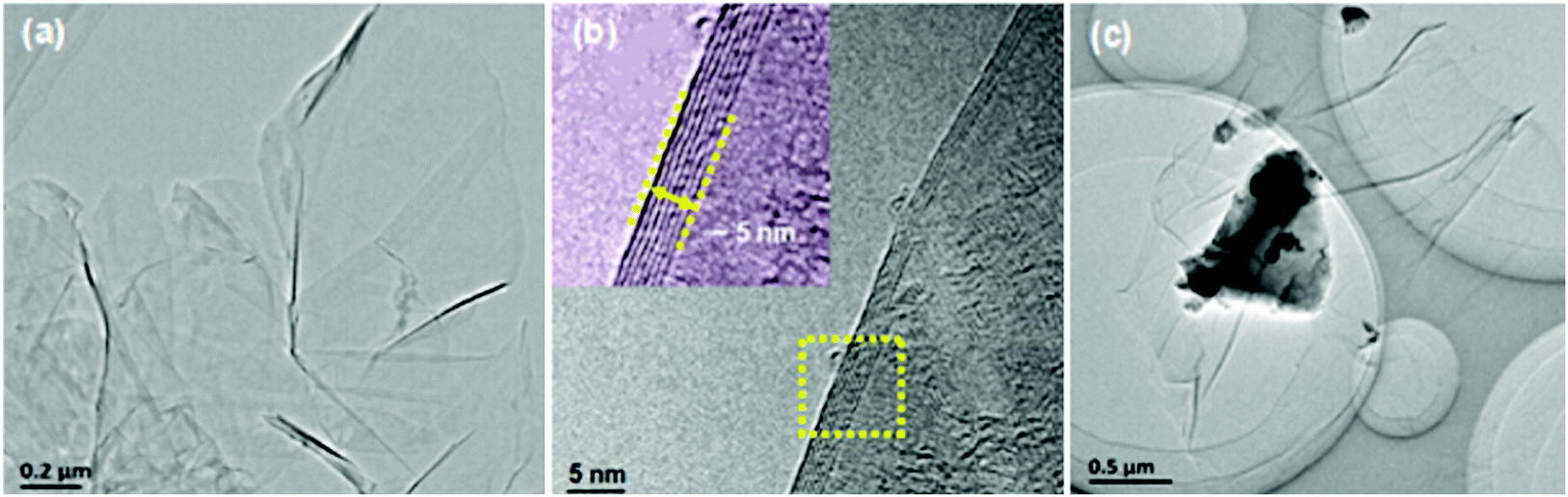 | ||
| Fig. 1 (a and b) Low and high-magnified TEM of the as prepared GO; the inset in (b) is the magnified edge of GO, indicating an edge thickness of ∼5 nm. (c) Low-magnified TEM of Ce0.85Fe3CoSb12/rGO particle wrapping morphology. | ||
A TEM image reveals that the matrix particles in the final microstructure are distinctly surrounded by rGO nano-layers (Fig. 2a). High-magnification TEM images of the Ce0.85Fe3CoSb12/rGO (0.56, 1.4 vol%) samples show particles separated by rGO layers of ∼2–6 nm (Fig. 2b and c). Comparatively, the average thickness of the rGO layers for the 2.8 vol% rGO sample is greater than 10 nm (see Fig. S5, ESI†). Though a full 3D characterization of the rGO distribution in the bulk composite remains a problem, we can infer its 3D distribution from 2D sectional images. High angle annular dark-field imaging (HAADF) shows rGO wrapping the skutterudite grains in Fig. 3. The rGO appears interconnected, constructing a continuous network along the grain boundaries (reconfirmed by EDS analysis), seen in bright white in Fig. 3 (left). Two more HAADF images are shown in Fig. S7 (ESI†) to further verify this observation in different regions of the sample.
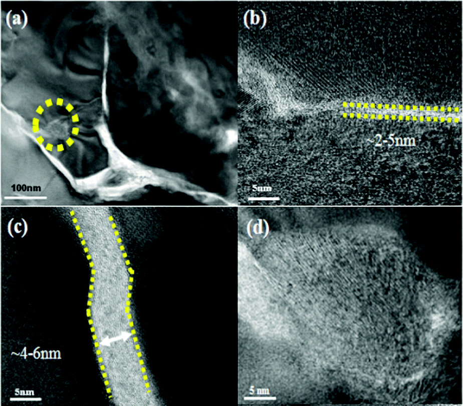 | ||
| Fig. 2 (a) Low-magnified TEM cross-section image of Ce0.85Fe3CoSb12/0.56 vol% rGO sample, (b and c) high-magnified TEM cross-section image of Ce0.85Fe3CoSb12/0.56, 1.4 vol% rGO samples, (d) high-magnified TEM cross-section image of the yellow circled area in (a). | ||
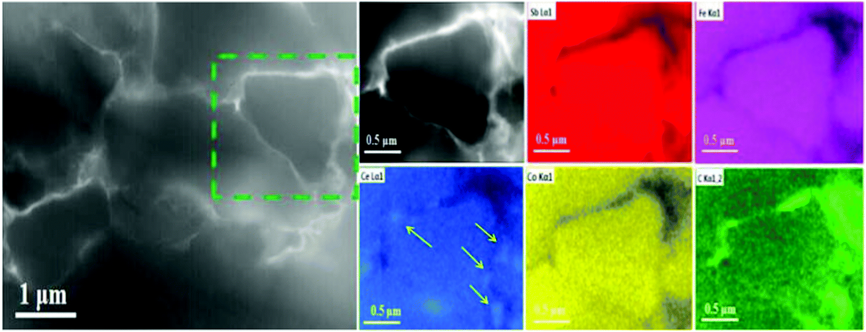 | ||
| Fig. 3 HAADF-STEM image of the p-type Ce0.85Fe3CoSb12/0.56 vol% rGO wrapping sample. Right inset: Local energy spectrum analysis for Sb, Fe, Ce, Co and C respectively. | ||
Fig. 2d shows CeO2 nano-precipitates (confirmed by EDS as shown in Fig. S6, ESI†) marked by the yellow circle in Fig. 2a, which are presumably generated during the SPS process. Ce-rich nano-precipitates at grain boundaries were also observed in the HAADF image in Fig. 3, as marked by yellow arrows, further indicating formation of CeO2 at grain boundaries. Of all the component elements of the matrix material, the filler element Ce is the most chemically active element. During SPS, oxygen from the rGO presumably reacts with Ce to form a small amount of ∼20–40 nm sized CeO2 precipitates.
Electric transport
The electrical conductivities of samples containing small amounts of rGO (y = 0.56 and 1.4 for p-type and y = 0.72 for n-type) are only slightly decreased (Fig. 4a) compared to the samples without graphene, indicating that thin layers of rGO at grain boundaries have minimal effect on electronic properties. This minimal effect on charge carrier mobility is confirmed in Fig. 4b. Further increasing the rGO content leads to more noticeable reduction in mobility when rGO content reaches 2.8 vol%.30,38,39 Likewise, the Seebeck coefficients and power factors as a function of temperature (Fig. 4c and d) are essentially unchanged for small contents of rGO. This is consistent with Hall effect measurements (Table S1, ESI†). The p-type Ce0.85Fe3CoSb12 shows only a slight increase in hole concentration, which should result from the generation of the small amount of CeO2 nano-precipitates seen in the TEM.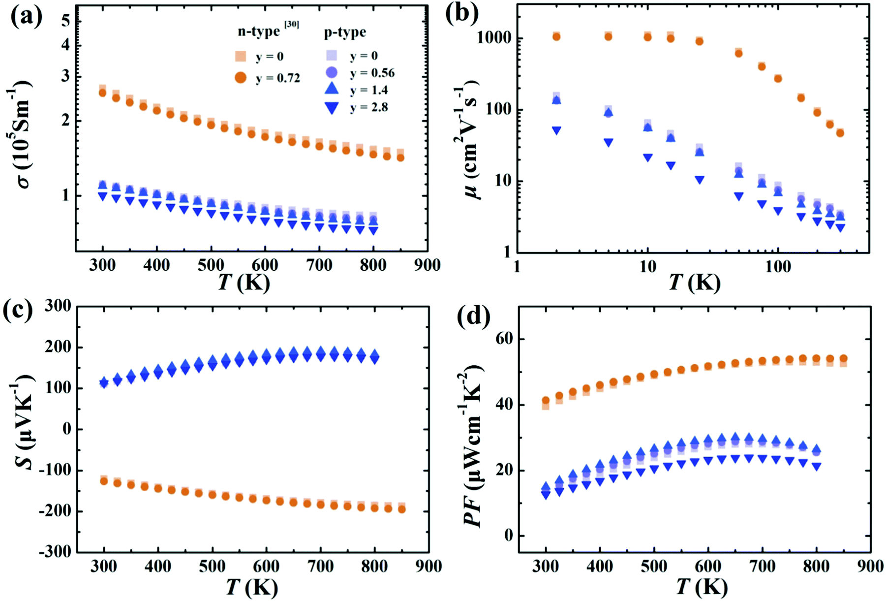 | ||
| Fig. 4 Temperature dependence of the (a) electrical conductivity, (b) carrier mobility, (c) Seebeck coefficients, (d) power factors of p-type Ce0.85Fe3CoSb12/y vol% rGO samples (y = 0, 0.56, 1.4, 2.8) and n-type Yb0.27Co4Sb12/y vol% samples (y = 0, 0.72) from ref. 30. | ||
Thermal conductivity
The total thermal conductivity (κtot) shown in Fig. 5a contains contributions from charge carriers through electronic (κe) and bipolar (κBP) conduction, and from the lattice (κlat), whereby, κtot = κe + κBP + κlat. The κtot values of the pristine p-type skutterudite Ce0.85Fe3CoSb12 sample agrees well with previously reported data of CeyFe3CoSb12.16Fig. 5b shows κlat + κBP where κe was calculated using the Wiedemann–Franz law with experimental σ values and L = 2 × 10⁻⁸ W Ω K−2. Introduction of rGO into the grain boundaries (GB) of skutterudite significantly reduces κlat initially, but then increases with increasing amounts of rGO. This behavior is observed in both p-type and n-type skutterudite.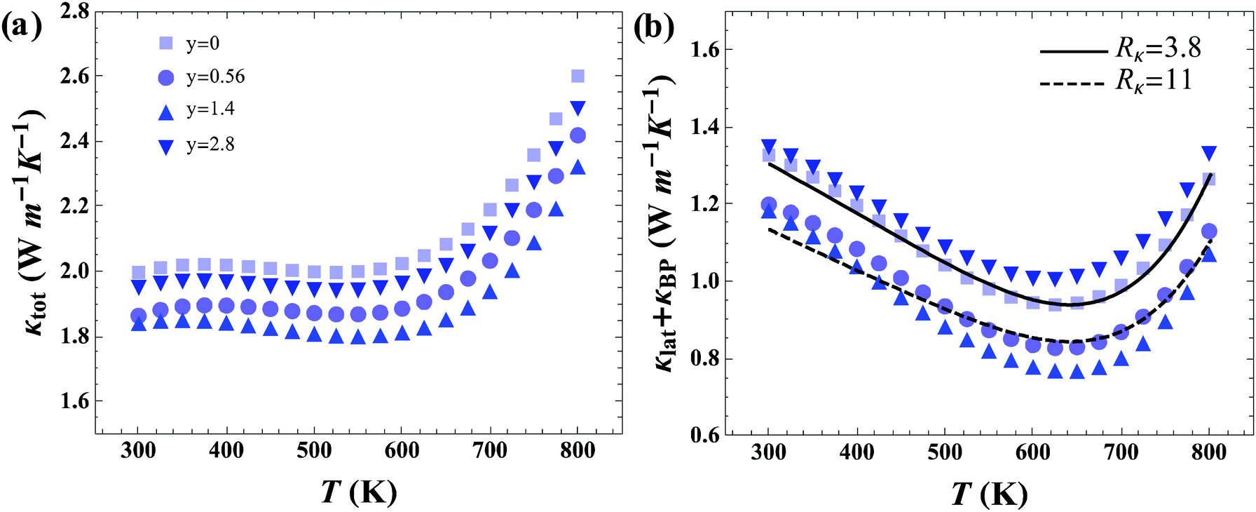 | ||
| Fig. 5 Temperature dependence of (a) κtot and (b) κlat + κBP for Ce0.85Fe3CoSb12 with varying amounts of rGO. Lines are modeled κlat + κBP for 0 vol% rGO (solid) and 0.56 vol% rGO (dashed). The interfacial thermal resistance, Rκ, is in units of 10−7 m2 K W−1. | ||
In order to clarify the effect of the three-dimensional rGO network, a phenomenological model for thermal conduction in these composite systems was constructed. Through this model the interfacial thermal resistance, Rκ, was determined for materials without rGO and compared to those containing an rGO network. The lattice thermal conductivity of the n and p-type skutterudite with varying average grain sizes (![[d with combining macron]](https://www.rsc.org/images/entities/i_char_0064_0304.gif) ) was modeled to determine the interfacial thermal resistance (for a unit area) with Rκ = 1/G, where G is the interfacial thermal conductance (per unit area). We think of Rκ as including all aspects of the GB complexion for transport perpendicular to the interface including effects between the skutterudite and graphene (interface effects) as well as thermal resistance across the graphene.§ More characterization on this GB complexion would be required to gain a mechanistic understanding.
) was modeled to determine the interfacial thermal resistance (for a unit area) with Rκ = 1/G, where G is the interfacial thermal conductance (per unit area). We think of Rκ as including all aspects of the GB complexion for transport perpendicular to the interface including effects between the skutterudite and graphene (interface effects) as well as thermal resistance across the graphene.§ More characterization on this GB complexion would be required to gain a mechanistic understanding.
The bulk thermal conductivity (κbulk) is fit empirically along with a constant Rκ for samples without graphene of various grain sizes. This κbulk will then include all the relevant phonon–phonon, electron–phonon, and point defect scattering processes. Here we use a simple model40 of cubic grains with edge length where the linear density of interfaces is the inverse of the average grain size, 1/. The method used here for determining Rκ is similar to that used in by Yang et al. on yttria-stabilized zirconia (see eqn (5) in ref. 40). The lattice thermal conductivity of polycrystalline samples is then fit to
| κpoly−1 = κbulk−1 + Rκ/. | (1) |
Fig. 6 shows the results of modeling the grain size dependent data sets. As can be seen in Fig. 6a and c, n-type and p-type skutterudite materials in this study have the same value of Rκ = 3.8 × 10⁻⁷ m2 K W−1 (without graphene) as could be expected from similarities in crystal structure, chemical species, and processing methods.
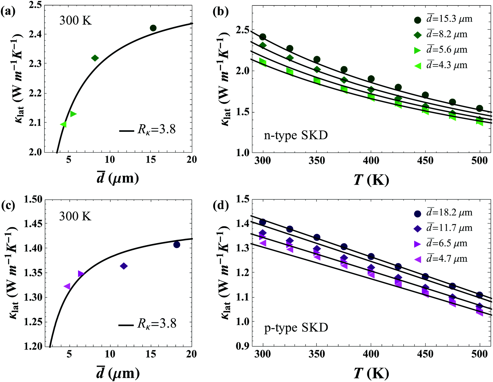 | ||
| Fig. 6 Determination of interfacial thermal resistance from grain boundaries in polycrystalline skutterudite samples (without rGO). The uncertainty in the grain-size is ∼20%. (a and c) Show room temperature lattice thermal conductivity with varying grain size. Rκ is in units of 10−7 m2 K W−1; (b and d) show κlat with temperature for n and p-type skutterudite samples. Lines in all figures are calculated from eqn (1). | ||
For the system with multilayer graphene, thermal transport through the in-plane direction of the graphene layer of thickness, t, must be included due to the high thermal conductivity of graphite (5 W m−1 K−1 in the c-direction and 2000 W m−1 K−1 in the a and b-directions at 300 K41).
Using the parallel conductance model depicted in Fig. 7 the thermal conductivity of the composite system, for t ≪ , is given by
 | (2) |
of the samples ( , again for t ≪ ). While TEM images in Fig. 2 give a measurement of rGO thickness, this is a very local measurement and the geometrical approach is thought to embody a more average representation of the composite system.
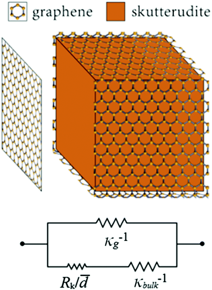 | ||
| Fig. 7 Diagram of the thermal circuit representing the thermal resistance of grain boundaries wrapped in graphene with the resistance elements labeled by their respective thermal resistivities. | ||
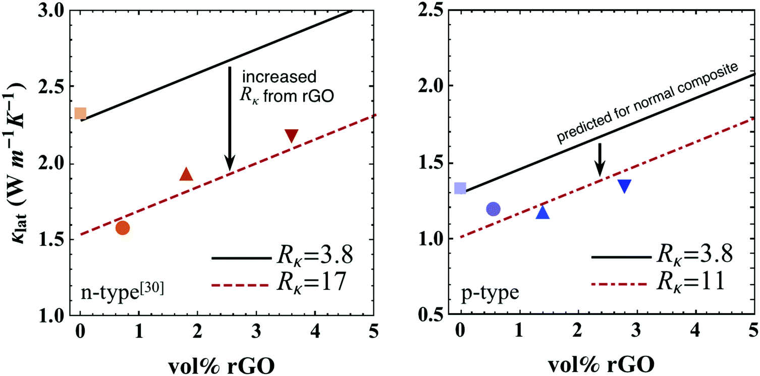 | ||
| Fig. 8 Lattice thermal conductivity (κlat) at 300 K with varying amounts of rGO for both n and p-type skutterudite/rGO composite (solid symbols). Data for n-type material are from ref. 30. Upon the introduction of rGO, κlat (solid lines) predicted via the thermal circuit model in eqn (2) with Rκ = 3.8 × 10⁻⁷ m2 K W−1 (assuming unchanged boundary complexion), κlat (dashed lines) calculated via the thermal circuit model in eqn (2) with fitted Rκ values (17 × 10−7 m2 K W−1 for n-type and 11 × 10−7 m2 K W−1 for p-type). | ||
The interfacial thermal resistance, Rκ, of skutterudite with rGO can now be determined by fitting the data in Fig. 8. The resultant value of Rκ at 300 K was increased by nearly a factor of 3 for p-type and 5 for n-type samples containing rGO. From Fig. 8, it is clearly seen that the rise in thermal conductivity for higher volume fractions of rGO is explained by the parallel thermal conductance of graphene around the grains. Thicker multi-layer graphene causes thermal shorting around the skutterudite grains, increasing the thermal conductivity as the volume fraction of rGO increases.¶ For the most reduction in thermal conductivity of the composite, thinner graphene layers should be used. This model can also be extended to higher temperatures where the predicted κlat is calculated through eqn (2) with appropriate values of Rκ (from Fig. 6 and 8) where the bipolar term, κBP was calculated with the general form, κBP ∝ exp(−Eg/2kBT).
Thermoelectric figure of merit and module performance
Fig. 9 shows the temperature dependence of zT for p-type Ce0.85Fe3CoSb12/y vol% rGO (y = 0, 0.56, 1.4, 2.8) samples and n-type Yb0.27Co4Sb12/y vol% rGO (y = 0, 0.72) samples from ref. 30. All p-type sample zTs first increase with temperature and then drop after reaching a peak at ∼700 K. This is due to the decrease of power factor and rapid increase of thermal conductivity when T ≥ 650 K, which is attributed to bipolar conduction. Compared to samples without graphene, zTs for p-type samples with y ≤ 1.4 exhibit robust increases due to the increased thermal resistance of the grain boundaries. The y = 1.4 p-type sample attains a peak zT of 1.06 at 700 K, while n-type rGO sample attains a peak of 1.51 at 850 K.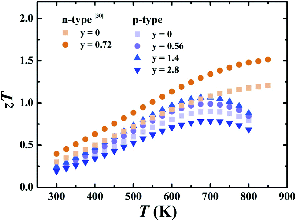 | ||
| Fig. 9 Temperature-dependent zT for Ce0.85Fe3CoSb12/y vol% rGO (y = 0, 0.56, 1.4, 2.8) samples from 300–800 K and Yb0.27Co4Sb12/y vol% (y = 0, 0.72) samples from 300–850 K from ref. 30. | ||
The p-type Ce0.85Fe3CoSb12/1.4 vol% rGO and n-type Yb0.27Co4Sb12/0.72 vol% rGO30 composite bulk were used to fabricate a thermoelectric module with dimension of 20 mm × 20 mm × 16 mm as shown in Fig. 10a. A module consisting of 8 n–p couples were assembled via SPS, spark cutting, and welding.32 For comparison, a reference thermoelectric module was also fabricated by using pristine n-type Yb0.27Co4Sb12 and p-type Ce0.85Fe3CoSb12 bulk materials without rGO. Based on PEM-3 measurement, under hot/cold-side temperature 873 K/296 K, a high conversion efficiency of 8.4% and maximum power output of 3.8 W were obtained, which is significantly higher than 6.8% and 3.1 W of the pristine skutterudite module, further verifying that the skutterudite/rGO nanocomposite has improved performance. It is the first time that a module with n and p-type legs both made of skutterudite nanocomposite was fabricated. The measured conversion efficiency of 8.4% (ΔT = 577 K) is among the highest of all reported values not only for skutterudite based modules,33–35 but also other TE material systems.43,44 The ANSYS-simulated ideal, theoretical conversion efficiency44 (dash line in Fig. 10b) of the skutterudite/rGO module is 10.5%, based on the measured thermoelectric properties. The 25% lower device performance can be attributed to interfacial thermal and electrical resistance between the thermoelectric material and the metallized ceramic substrate, as well as convection and radiation losses and is typical for such devices.
 | ||
| Fig. 10 (a) Thermoelectric module with dimension of 20 mm × 20 mm × 16 mm using Ce0.85Fe3CoSb12/1.4 vol% rGO and Yb0.27Co4Sb12/0.72 vol% rGO composite as p and n-type legs, respectively; (b) maximum conversion efficiency and power output as a function of Th for the skutterudite/rGO based modules (M-SKD/rGO) and the reference device made of pure SKD (M-SKD). The dash lines represent the theoretical conversion efficiency of M-SKD/rGO with a maximum value of 10.5%, and M-SKD with a maximum value of 8.0%, when ignoring electrical and thermal contact resistances. | ||
Conclusions
Not all grain boundaries scatter phonons equivalently. Here, it was shown that introducing multilayer graphene into grain boundaries of thermoelectric skutterudite dramatically increases the thermal boundary resistance. When this three dimensional rGO network in the GBs is kept thin (∼2–6 nm for 1.4 vol% rGO), κlat is reduced by ∼20% and the electrical properties are essentially unchanged, resulting in improved zT. Additionally, thermal shorting via thermal conduction through the high κlat rGO layers is also avoided. This effect has been seen in both n and p-type SKD/rGO composites and a TE module consisting of 8 n–p couples was made and characterized to demonstrate the improved efficiency. It is the first time a module using n and p-type skutterudite nanocomposite has been made, and its conversion efficiency of 8.4% is among the highest of any value reported for TE modules33–35,43,44Methods
Material synthesis
Highly pure elements of Ce (99.98%), Fe (99.99%), Co (99.99%) and Sb (99.9999%) were used as the raw material to prepare Ce0.85Fe3CoSb12. The raw materials were stoichiometrically weighed and sealed in quartz tubes, in which the inner walls were coated with carbon. All the above procedure was performed in a high-purity-Ar-filled glove box. The element mixtures were heated at a speed of 4 K min−1 to 1373 K, remained at this temperature for 24 h to ensure complete melting of all elements before being quenched into a water bath and then annealed at 923 K for 7 days. The obtained ingots were crushed into fine powders. Purified natural graphite (SP-1, Bay Carbon) was use to synthesize GO according to the improved Hummers method. Fine 1.5 g Ce0.85Fe3CoSb12 powder was firstly dispersed in 200 ml deionized water, then added with 0.05 mg ml−1 GO water suspension solution dropwise, followed by ultrasonic mixing for 30 min. The mixture then underwent vacuum filtering and drying at 363 K in Ar-5 vol% H2 gas flow for 4 h. The resultant material was regrinded into fine powder. The composite powders were then loaded into a graphite die and consolidated by spark plasma sintering (Sumitomo SPS-2040) in vacuum at 873 K for 15 minutes under a pressure of 55 MPa, yielding fully densified bulk disk-shaped samples CeyFe3CoSb12/y vol% rGO, with different rGO content (y = 0, 0.56, 1.4, 2.8).Structural characterization
The powder constituent phase was determined with X-ray diffractometry (CuKα, Rigaku, Rint 2000) equipped with CuKα radiation (λ = 1.5418 Å). The morphology and microstructure were investigated with transmission electron microscopy (TEM) on a JEM 2010 microscope. Traditional standard TEM specimen preparation processes were used to prepare the thin TEM specimens, consisting of cutting, grinding, mechanical polishing and low-voltage (1.5 V) Ar-ion milling on a liquid nitrogen cooling stage. The thin TEM specimens were nitrogen plasma cleaned for 30 s, then used for scanning transmission electron microscopy (STEM) investigation (FEI Magellan 400) with an accelerating voltage of 30 kV. The grain size of samples with varying rGO content was determined from cross-sectional SEM micrographs. The intercept technique was used to determine the average grain size—the number of intersection points between grain boundaries and a randomly drawn line segment through the micrograph is counted and divided into the length of the random line segment. ∼60 line segments were used on each micrograph to obtain good statistics. The uncertainty in grain size (±20%) is due to limited definition in the outline of grain boundaries, sampling statistics, and the fact that only localized regions of samples are considered in each micrograph.Electrical properties
ULVAC-RIKO ZEM-3 instrument system was adopted to concurrently measure the electrical conductivity (σ) and Seebeck coefficient (S) from 300 to 800 K in a helium atmosphere on rectangular bars with dimensions of ∼8 mm × 2 mm × 2 mm cut from the SPSed disc-samples. PPMS-Quantum Design was used to characterize the low temperature electrical property on bars with dimension of ∼6 mm × 2 mm × 1 mm cut from the SPSed disc-samples. The hall resistance (Rh) was measured with a five-probe configuration under a magnetic field of −3 to 3 T in both negative and positive magnetic field directions to minimize the joule resistive errors. The hole mobility (μH) and carrier concentration (p) were calculated from p = 1/Rhe and μH = σ/pe, where e is the elementary charge and σ is the electrical conductivity.Thermal conductivity
Thermal diffusivity was measured on disc-samples of ∼1–2 mm thick and 10 mm in diameter prepared by grinding and polishing the SPSed pellets. To minimize errors on the emissivity of the samples, both sides of the coin-samples was sprayed with a thin graphite layer. The total thermal conductivity (κtot) was calculated via κtot = ρCpλ, hereinto, ρ is density of the disc-samples determined by Archimedes method (METTLER TOLEDO AB104-L), Cp is the specific heat determined by differential scanning calorimetry (DSC 404C, Netzsch, Germany). λ is the thermal diffusivity coefficient measured on Netzsch LFA-427 instrument by using laser flash diffusivity method (laser voltage: 450 V, pulse width: 0.5 ms). The Cape–Lehman method with pulse correction was used to analyze the thermal diffusivity data.Thermoelectric module fabrication and performance
Yb0.27Co4Sb12/0.72 vol% rGO was used as the n-type leg material, and the Ce0.85Fe3CoSb12/1.4 vol% rGO as the p-type leg material. The SPSed cylindrical bulks were cut into legs of 4 mm × 4 mm × 12 mm via spark cutting for module assembly. The n and p-type legs were then connected to Mo50Cu50 electrode using Ag–Cu–Zn welding alloy. The cold side of the module adopted copper clad ceramic substrates for connection of couples, using low temperature Pb–Sb welding alloy. The modules contained a total of 16 legs, joining into 8 n–p couples, all connected electrically in series and thermally in parallel. The PEM-3 testing system (ULVAC-RIKO, Inc.) was used for measurement of the power output, internal resistance and energy conversion efficiency of the modules. The hot-side temperature was changed from 473 K to 873 K, while the circulation water at the cold side was kept at 283 K.Author contributions
L. C. and P. Z. conceived and designed the experiments. P. Z., Y. T. and J. L. performed the experiments. G. J., R. H. and M. D. constructed the model. G. J., L. C., R. H., P. Z., Q. Z. analyzed the data. R. H., G. J., L. C. and P. Z. wrote the manuscript. All authors discussed the results and commented on the manuscript.Competing financial interests
The authors declare no competing financial interests.Acknowledgements
This work was supported by the National Natural Science Foundation of China (no. 51222209 and no. 11234012) and 973 Program of National Basic Research Program of China (no. 2013CB632503 and no. 51402337). Solid-State Solar-Thermal Energy Conversion Center (S3TEC), an Energy Frontier Research Center funded by the U.S. Department of Energy, Office of Science, Basic Energy Sciences under Award # DE-SC0001299 and NSF DMR program Grant No. 1334713 and 1333335.References
- M. S. Dresselhaus, G. Chen, M. Y. Tang, R. G. Yang, H. Lee, D. Z. Wang, Z. F. Ren, J. P. Fleurial and P. Gogna, Adv. Mater., 2007, 19, 1043 CrossRef CAS.
- J. R. Sootsman, D. Y. Chung and M. G. Kanatzidis, Angew. Chem., Int. Ed., 2009, 48, 8616 CrossRef CAS PubMed.
- G. J. Snyder and E. S. Toberer, Nat. Mater., 2008, 7, 105 CrossRef CAS PubMed.
- Y. Pei, X. Shi, A. LaLonde, H. Wang, L. Chen and G. J. Snyder, Nature, 2011, 473, 66 CrossRef CAS PubMed.
- C. J. Vineis, A. Shakouri, A. Majumdar and M. G. Kanatzidis, Adv. Mater., 2010, 22, 3970 CrossRef CAS PubMed.
- T. Basu and M. Ray, Int. J. Nanotechnol., 2014, 11, 897–909 CrossRef CAS.
- S. Ballikaya, H. Chi, J. R. Salvador and C. Uher, J. Mater. Chem. A, 2013, 1, 12478 CAS.
- S. I. Kim, K. H. Lee, H. A. Mun, H. S. Kim, S. W. Hwang, J. W. Roh, D. J. Yang, W. H. Shin, X. S. Li, Y. H. Lee, G. J. Snyder and S. W. Kim, Science, 2015, 348, 109 CrossRef CAS PubMed.
- G. J. Snyder, M. Christensen, E. Nishibori, T. Caillat and B. B. Iversen, Nat. Mater., 2004, 3, 458 CrossRef CAS PubMed.
- B. C. Sales, D. Mandrus and R. K. Williams, Science, 1996, 272, 1325 CAS.
- B. C. Sales, D. Mandrus, B. C. Chakoumakos, V. Keppens and J. R. Thompson, Phys. Rev. B: Condens. Matter Mater. Phys., 1997, 56, 15081 CrossRef CAS.
- G. S. Nolas, M. Kaeser, R. T. Littleton and T. M. Tritt, Appl. Phys. Lett., 2000, 77, 1855 CrossRef CAS.
- L. D. Chen, T. Kawahara, X. F. Tang, T. Goto, T. Hirai, J. S. Dyck, W. Chen and C. Uher, J. Appl. Phys., 2001, 90, 1864 CrossRef CAS.
- X. Shi, J. Yang, R. J. Salvador, M. F. Chi, Y. J. Cho, H. Wang, S. Q. Bai, J. H. Yang, W. Q. Zhang and L. D. Chen, J. Am. Chem. Soc., 2011, 133, 7837 CrossRef CAS PubMed.
- G. Rogl, A. Grytsiv, P. Rogl, N. Peranio, E. Bauer, M. Zehetbauer and O. Eibl, Acta Mater., 2014, 63, 30–43 CrossRef CAS.
- R. H. Liu, J. Yang, X. H. Chen, X. Shi, L. D. Chen and C. Uher, Intermetallics, 2011, 19, 1747 CrossRef CAS.
- L. D. Chen, Z. Xiong and S. Q. Bai, J. Inorg. Mater., 2010, 25, 561 CrossRef CAS.
- N. A. Heinz, T. Ikeda, Y. Z. Pei and G. J. Snyder, Adv. Funct. Mater., 2014, 24, 2135 CrossRef CAS.
- D. J. Bergman and O. Levy, J. Appl. Phys., 1991, 70, 6821 CrossRef.
- S. J. Poon, A. S. Petersen and D. Wu, Appl. Phys. Lett., 2013, 102, 173110 CrossRef.
- H. S. Kim, S. D. Kang, Y. L. Tang, R. Hanus and G. J. Snyder, Mater. Horiz., 2016, 3, 234 RSC.
- F. Chen, Y. Li, G. Gao, F. Yao, K. Wang, J. Li, X. Li, X. Gao and W. Wu, J. Am. Ceram. Soc., 2015, 98, 1372–1376 CrossRef CAS.
- S. I. Kim, K. H. Lee, H. A. Mun, H. S. Kim, S. W. Hwang, J. W. Roh, D. J. Yang, W. H. Shin, X. S. Li, Y. H. Lee, G. J. Snyder and S. W. Kim, Science, 2015, 348, 109 CrossRef CAS PubMed.
- P. R. Cantwell, M. Tang, S. J. Dillon, J. Luo, G. S. Rohrer and M. P. Harmer, Acta Mater., 2014, 62, 1–48 CrossRef CAS.
- Y. Lin, C. Norman, D. Srivastava, F. Azough, L. Wang, M. Robbins, K. Simpson, R. Freer and I. Kinloch, ACS Appl. Mater. Interfaces, 2015, 7, 15898–15908 CAS.
- H. Ju, M. Kim and J. Kim, Chem. Eng. J., 2015, 275, 102 CrossRef CAS.
- H. J. Chen, C. Y. Yang, F. Q. Huang, H. L. Liu, G. H. Zhang and D. Y. Wan, CrystEngComm, 2013, 15, 6648 RSC.
- B. Feng, J. Xie, G. S. Cao, T. J. Zhu and X. B. Zhao, J. Mater. Chem. A, 2013, 1, 13111 CAS.
- J. D. Dong, W. Liu, H. Li, X. L. Su, X. F. Tang and C. Uher, J. Mater. Chem. A, 2013, 1, 12503 CAS.
- P. A. Zong, X. H. Chen, Y. W. Zhu, Z. W. Liu, Y. Zeng and L. D. Chen, J. Mater. Chem. A, 2015, 3, 8643 CAS.
- L. Luo, J. Wu, J. Luo, J. Huang and V. P. Dravid, Sci. Rep., 2014, 4, 3863 Search PubMed.
- Y. S. Tang, S. Q. Bai, D. D. Ren, J. C. Liao, L. T. Zhang and L. D. Chen, J. Inorg. Mater., 2015, 30, 256 CrossRef CAS.
- T. Ochi, G. Nie, S. Suzuki, M. Kikuchi, S. Ito and J. Q. Guo, J. Electron. Mater., 2014, 43, 2344 CrossRef CAS.
- J. R. Salvador, J. Y. Cho, Z. X. Ye, J. E. Moczygemba, A. J. Thompson, J. W. Sharp, J. D. Koenig, R. Maloney, T. Thompson, J. Sakamoto, H. Wang and A. A. Wereszczak, Phys. Chem. Chem. Phys., 2014, 16, 12510 RSC.
- Q. H. Zhang, X. Y. Huang, S. Q. Bai, X. Shi, C. Uher and L. D. Chen, Adv. Eng. Mater., 2016, 18, 194–213 CrossRef CAS.
- Y. C. Fan, W. Jiang and A. Kawasaki, Adv. Funct. Mater., 2012, 22, 3882 CrossRef CAS.
- P. Harshit, G. Salvatore, K. M. Mahesh and J. R. Mike, J. Eur. Ceram. Soc., 2014, 34, 3357–3364 CrossRef.
- J. S. Dyck, W. D. Chen, C. Uher, L. Chen, X. F. Tang and T. Hirai, J. Appl. Phys., 2002, 91, 3698 CrossRef CAS.
- J. Yang, G. P. Meisner, C. J. Rawn, H. Wang, B. C. Chakoumakos, J. Martin, G. S. Nolas, B. L. Pedersen and J. K. Stalick, J. Appl. Phys., 2007, 102, 083702 CrossRef.
- H. S. Yang, G. R. Bai, L. J. Thompson and J. A. Eastman, Acta Mater., 2002, 50, 2309–2317 CrossRef CAS.
- E. Pop, V. Varshney and A. Roy, MRS Bull., 2012, 1273, 1–28 Search PubMed.
- D. D. L. Chung, J. Mater. Sci., 2002, 37(8), 1475–1489 CrossRef CAS.
- X. K. Hu, P. Jood, M. Ohta, M. Kunii, K. Nagase, H. Nishiate, M. G. Kanatzidis and A. Yamamoto, Energy Environ. Sci., 2016, 9, 517–529 CAS.
- C. G. Fu, S. Q. Bai, Y. T. Liu, Y. S. Tang, L. D. Chen, X. B. Zhao and T. J. Zhu, Nat. Commun., 2015, 6, 8144 CrossRef PubMed.
Footnotes |
| † Electronic supplementary information (ESI) available. See DOI: 10.1039/c6ee02467j |
| ‡ These authors contributed equally to this work. |
| § Phonon scattering off of rGO/SKD interfaces parallel to the direction of propagation (specular effects) are neglected. |
| ¶ This ‘shorting’ effect was not observed in electrical conductivity measurements because the in-plane electrical conductivity of graphite (2.26 × 10⁴ S cm−1,42) is smaller than that of n-type and p-type SKD in this study. |
| This journal is © The Royal Society of Chemistry 2017 |