
Superflexible, high-efficiency perovskite solar cells utilizing graphene electrodes: towards future foldable power sources†
Jungjin
Yoon‡
ab,
Hyangki
Sung‡
c,
Gunhee
Lee
ab,
Woohyung
Cho
a,
Namyoung
Ahn
ab,
Hyun Suk
Jung
*d and
Mansoo
Choi
*ab
aGlobal Frontier Center for Multiscale Energy Systems, Seoul National University, Seoul, 08826, Republic of Korea. E-mail: mchoi@snu.ac.kr
bDepartment of Mechanical and Aerospace Engineering, Seoul National University, Seoul 08826, Republic of Korea
cSamsung Display Co., Ltd, Asan 31454, Republic of Korea
dSchool of Advanced Materials Science and Engineering, Sungkyunkwan University, Suwon 16419, Republic of Korea. E-mail: hsjung1@skku.edu
First published on 10th November 2016
Abstract
With rapid and brilliant progress in performance over recent years, perovskite solar cells have drawn increasing attention for portable power source applications. Their advantageous features such as high efficiency, low cost, light weight and flexibility should be maximized if a robust and reliable flexible transparent electrode is offered. Here we demonstrate highly efficient and reliable super flexible perovskite solar cells using graphene as a transparent electrode. The device performance reaches 16.8% with no hysteresis comparable to that of the counterpart fabricated on a flexible indium-tin-oxide electrode showing a maximum efficiency of 17.3%. The flexible devices also demonstrate superb stability against bending deformation, maintaining >90% of its original efficiency after 1000 bending cycles and 85% even after 5000 bending cycles with a bending radius of 2 mm. This overwhelming bending stability highlights that perovskite photovoltaics with graphene electrodes can pave the way for rollable and foldable photovoltaic applications.
Broader contextRecently, flexible perovskite solar cells have been actively investigated to realize an efficient portable power source. Generally, the architecture of these flexible devices is based on ITO-coated flexible plastic substrates, and, unfortunately, the power conversion efficiency of ITO-based flexible perovskite solar cells tends to degrade drastically under harsh bending conditions with a bending radius of ∼4 mm due to the generation of cracks on the brittle ITO. Here, we fabricated flexible perovskite solar cells by utilizing monolayer graphene as a transparent electrode. The graphene-based flexible perovskite solar cells exhibited a maximum power conversion efficiency of 16.8% with no hysteresis. After 5000 bending cycles with bending radii of 4 and 2 mm, the graphene-based devices maintained over 85% of their initial power conversion efficiency. Given this superior bending robustness, graphene-based perovskite solar cells will pave the way towards foldable and wearable power applications. |
Introduction
Organolead halide perovskite solar cells have been establishing their position as promising next-generation solar devices, showing a brilliant improvement in power conversion efficiency (PCE) from 3.8% to >20% over the past 5 years.1–5 In particular, they are expected to become an effective power source for portable and wearable devices due to their high specific power density and flexibility.6,7Perovskite solar cells generally adopt either a mesoporous TiO2 or planar heterojunction structure. The structure with a mesoporous TiO2 scaffold is a well-established design in perovskite solar cells, achieving the record-high PCE of over 20%.5 However, a high temperature process at over 450 °C is required to form mesoporous TiO2, which is not compatible with flexible polymer substrates.8 In order to realize the benefits of perovskite solar cells with polymer substrates, low-temperature-processable perovskite solar cells with a planar heterojunction configuration have been actively investigated by utilizing organic semiconductors or flat metal oxide films as charge extractors or blocking layers, which can be fabricated at a low temperature.9–12 In 2013, Docampo et al. demonstrated the first flexible perovskite solar cells with a PCE of 6.4% by adopting an inverted device architecture with low-temperature solution-processed charge collection layers.13 In 2015, Kim et al. introduced a compact TiOx layer to flexible perovskite solar cells using a low-temperature processable atomic layer deposition method, and achieved a much improved PCE of 12.2%.6 In that report, the analysis on the device durability against repeated bending at various bending radii shows that the PCE decreases to 50% of its initial value after 1000 bending cycles at a bending radius of 4 mm, which is attributed to crack formation in the transparent conductive oxide (TCO) layer, indium tin oxide (ITO), during bending. It has been consistently observed in other studies that the PCE decreases to <60% of its initial value after 1000 bending cycles at a bending radius of <4 mm whenever ITO is used as a transparent conductive electrode.6,14
To avoid device degradation stemming from the brittle ITO, TCO-free flexible perovskite solar cells have been investigated by many research groups.15,16 Sun et al. used a conducting polymer, poly(3,4-ethylenedioxythiophene) polystyrene sulfonate (PEDOT:PSS), as a transparent electrode to replace the TCO electrodes in perovskite solar cells, and demonstrated that the PCE was maintained at ∼60% of its original value even after 2000 bending cycles with a bending radius of 2 mm.17 However, its PCE of 8.6% is considerably lower compared to that of the flexible perovskite solar cells fabricated on ITO electrodes reaching a maximum PCE of ∼16%.18–21 Recently, Li et al. demonstrated flexible perovskite solar cells utilizing an ultrathin silver-mesh/conducting polymer substrate with a PCE of 14.0% and high durability against mechanical deformation.7 The flexible device maintained a PCE at >95% of its initial value after 5000 bending cycles with a bending radius of 5 mm. However, non-uniform thermal conductivity of the hybrid electrode is likely to cause spatially non-homogeneous conversion of the perovskite precursor, and thus limits the formation of a high quality perovskite film. Therefore, in order to realize a perovskite solar cell with both excellent mechanical flexibility and high efficiency, it is essential for the electrode to be highly flexible, spatially homogeneous, electrically conductive, optically transparent, and durable against bending. In this respect, graphene, which possesses all these features, seems to be a very promising material for an efficient and robust transparent flexible electrode. Additionally, graphene is even light and easily available. Although single layer chemical vapor deposition (CVD) graphene generally has a high sheet resistance of over 1 kΩ sq−1,22 the resistance can be reduced to values as low as 30–500 Ω sq−1 by chemical doping or stacking of the graphene sheets.22–24
A graphene transparent electrode has already been demonstrated in flexible organic photovoltaics (OPVs) with a tandem structure, showing a record-high PCE of 8.48% among the TCO-free OPVs.25 The efficiency is, however, much lower than the 14.0% PCE of the perovskite-based TCO-free flexible solar cells.7 Very recently, our group has successfully demonstrated high-efficiency inverted perovskite solar cells with no hysteresis by using graphene as a transparent conducting anode instead of ITO, exhibiting a record-high PCE of 17.1% among TCO-free solar cells.26 However, the device is fabricated on a glass substrate, so flexible perovskite solar cells utilizing a graphene electrode and the analysis of their bending durability have not been demonstrated yet.
Here, we report high-efficiency perovskite-based flexible solar cells utilizing graphene as a transparent conducting electrode. Single layer CVD graphene transferred on a thin polyethylene naphthalate (PEN) film using a typical wet transfer process provides high flexibility and transmittance. Insufficient electrical conductivity of the single layer graphene on PEN is improved by thermally depositing a few-nanometer-thick molybdenum trioxide (MoO3) layer to induce hole doping in the graphene. As a result, the best PCE of 16.8% is achieved from the flexible device with no hysteresis. In addition, the device exhibits extremely great bending stability, maintaining a PCE of >90% of its original value after 1000 bending cycles with a bending radius of 2 mm as well as 4 mm. On the other hand, the PCE of the devices fabricated on ITO/PEN substrates for comparison decreases significantly to <40% of its initial value after 1000 bending cycles with a bending radius of 4 mm, although the devices exhibit a higher maximum PCE of 17.3% than those of the graphene-based devices before bending. To verify the bending stability of the graphene-based devices under harsher bending conditions, the devices are repeatedly bent over 1000 times at a bending radius of 2 mm, and surprisingly, the PCE is maintained at 85% of its initial value even after bending 5000 times. Neither significant cracks nor an increase in sheet resistance is observed in the graphene-based devices after repeated bending, contrary to the ITO-based devices. The bending stability at the bending radius of 2 mm demonstrates that the perovskite solar cells utilizing a graphene electrode can realize a reliable foldable photovoltaic device, exhibiting great potential for a paradigm change in solar cell utilization.
Results and discussion
Structure of graphene-based flexible perovskite solar cells
The structure of graphene-based flexible perovskite solar cells is schematically illustrated in Fig. 1. CH3NH3PbI3 (MAPbI3) was used as a perovskite absorber material, and organic materials such as PEDOT:PSS, fullerene (C60) and bathocuproine (BCP) were used as a hole transporting layer (HTL), an electron transporting layer (ETL), and a hole blocking layer (HBL), respectively. All the fabrication processes for those layers were carried out at temperatures below 110 °C to enable the photovoltaic devices to be formed on a flexible PEN substrate whose glass transition temperature is ∼120 °C. Single layer CVD graphene was utilized as a transparent anode rather than a cathode because the difference between the work function of graphene (4.46 eV) and the HOMO level of the PEDOT:PSS HTL (5.2 eV) was larger than that between the work function of graphene and the LUMO level of the C60 ETL (4.5 eV). Thus, when graphene was doped with charge carriers to have ohmic contact with adjacent organic charge-transporting layers, the use of graphene as an anode was beneficial to secure higher conductance.27,28 Taking into account that the work function of graphene can be adjusted by charge transfer interaction with either electron-donor or -acceptor molecules,29,30 a 2 nm-thick MoO3 layer was introduced between the graphene and the PEDOT:PSS layer via vacuum thermal evaporation to induce hole doping in the graphene (see Fig. S1, ESI†).31 In addition, the thin MoO3 layer changed the hydrophobic graphene surface to hydrophilic, so that the wettability of the PEDOT:PSS solution on the graphene surface could be improved.26 For the sake of simplicity in the subsequent discussion, the terms “Gr-Mo/PEN device” and “ITO/PEN device” will be used to refer to the flexible perovskite photovoltaic devices fabricated on PEN substrates utilizing the MoO3/graphene electrode and the ITO electrode, respectively.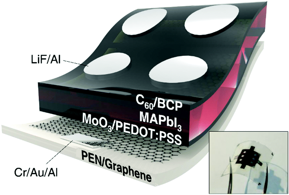 | ||
| Fig. 1 Device structure of graphene-based flexible perovskite solar cells (inset image: Photograph of a complete device). | ||
Fig. 2 shows the cross-sectional SEM images of the Gr-Mo/PEN device (Fig. 2(a)) and the ITO/PEN device (Fig. 2(b)). The images on the left-hand side and the right-hand side were measured in the secondary electron (SE) mode and the back-scattered electron (BSE) mode, respectively. As shown in Fig. 2(a), the PEDOT:PSS layer prepared from the PEDOT:PSS aqueous solution was well formed on the hydrophobic graphene surface, since the 2 nm-thick MoO3 interfacial layer rendered the hydrophobic graphene surface sufficiently hydrophilic. As a result, the subsequent perovskite layer was also uniformly fabricated on the Gr-Mo/PEN substrate with a similar thickness of ∼400 nm to that on the ITO/PEN substrate. In addition, the surface of the perovskite layers was observed to be quite smooth, which is in accordance with our previous reports for perovskite films fabricated using the Lewis base adduct method.32
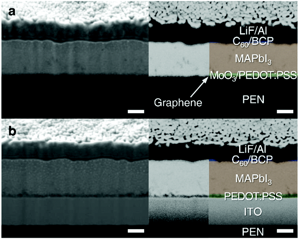 | ||
| Fig. 2 Cross-sectional images. (a and b) Focused ion-beam assisted SEM images of complete perovskite devices fabricated on (a) a Gr-Mo (MoO3-decorated graphene) electrode/PEN substrate and (b) an ITO electrode/PEN substrate. Both were measured in the SE mode (left) and the BSE mode (right) (scale bar, 200 nm). | ||
Performance of flexible perovskite solar cells
The photovoltaic properties of the Gr-Mo/PEN and ITO/PEN devices are summarized in Table 1 (all data in Table 1 were obtained from the device with an active area of 1.77 mm2). Noticeably, the PCE of the best-performing Gr-Mo/PEN device was obtained to be 16.8% with little hysteresis under an air mass of 1.5 global (AM 1.5G) upon one sun illumination at 100 mW cm−2, which is, to the best of our knowledge, the highest PCE among TCO-free flexible solar cells (see Table S1, ESI†). In addition, it should be noted here that this PCE value is high enough to be comparable to the 17.3% PCE of the best-performing ITO/PEN device. To realize graphene-based devices with high efficiency, it is important to optimize the HTLs (MoO3 and PEDOT:PSS). Due to the hydrophobic properties of graphene, the water-based PEDOT:PSS film coated on the pristine graphene/PEN substrate showed insufficient surface coverage (see Fig. S2(a), ESI†). On the other hand, the ultrathin MoO3 layer increased the wettability of PEDOT:PSS on the graphene surface to allow the PEDOT:PSS layer to be formed uniformly, as shown in Fig. S2(b) (ESI†). Fig. S2(c) and (d) (ESI†) show the J–V curves of the graphene-based flexible devices without and with MoO3, respectively. It is notable here that the devices with MoO3 exhibited consistent J–V characteristics, whereas those without MoO3 did not. Additionally, the devices using 2 nm-thick MoO3 only for the hole transporting layer (without PEDOT:PSS) were fabricated to check the hole transporting ability of MoO3 itself. The J–V curves of the devices presented poor performances as shown in Fig. S2(e) (ESI†), suggesting that only the layer of MoO3 without PEDOT:PSS could not be used as a HTL. Besides, the graphene-based device with a larger active area (9 mm2) was also demonstrated and the J–V curve of the device was depicted in Fig. S3 (ESI†). As a result, the large-sized device exhibited a PCE of 15.0%, which is similar to the average PCE of the smaller devices discussed in Table 1. This result suggests the feasibility of scaling up the graphene-based flexible devices.| Electrode | V OC (V) | J SC (mA cm−2) | FF | PCE (%) | |
|---|---|---|---|---|---|
| Gr-Mo/PEN | Average | 0.99 ± 0.02 | 21.0 ± 0.5 | 0.72 ± 0.03 | 15.0 ± 1.0 |
| Best | 1.00 | 21.7 | 0.78 | 16.8 | |
| ITO/PEN | Average | 0.97 ± 0.01 | 20.8 ± 0.5 | 0.81 ± 0.02 | 16.4 ± 0.5 |
| Best | 0.97 | 21.5 | 0.83 | 17.3 | |
Histograms for the PCEs of the Gr-Mo/PEN and ITO/PEN devices are shown in Fig. S4 (ESI†) and indicate the good reproducibility of the high efficiency devices, showing PCEs of over 15.0% and 16.4% for half of the Gr-Mo/PEN and ITO/PEN devices, respectively. Fig. 3(a) and (b) show the J–V curves of the best-performing Gr-Mo/PEN and ITO/PEN devices, respectively, measured via both forward and reverse bias sweeps. As already stated above, it can be seen here that both devices with different anode electrodes barely exhibited J–V hysteresis with respect to the scan direction, which was in agreement with the J–V behaviors of the inverted planar heterojunction perovskite solar cells reported in previous literatures.33,34 The stabilized JSC and PCE were demonstrated by holding the voltages at the maximum power points for each Gr-Mo/PEN and ITO/PEN device, respectively, as shown in Fig. S5 (ESI†). Comparing the J–V curves in Fig. 3(a) and (b), similar JSC values were observed for both types of device, but the series resistance of the Gr-Mo/PEN device was higher than that of the ITO/PEN device, resulting in the lower FF (FF = 0.78) of the Gr-Mo/PEN device than that of the ITO/PEN device (FF = 0.83), as described in Table 1.
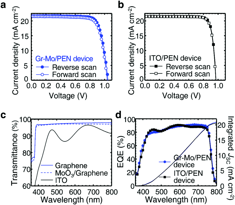 | ||
| Fig. 3 Photovoltaic performance and optical analysis. (a and b) J–V curves in reverse and forward scans measured under 100 mW cm−2 AM 1.5G illumination for the best-performing (a) Gr-Mo/PEN and (b) ITO/PEN devices. (c) Transmittance of the ITO/PEN, Gr/PEN, and Gr-Mo/PEN substrates. (d) EQE spectra of the Gr-Mo/PEN and ITO-PEN devices. | ||
Analysis of charge collection efficiency
In order to figure out how different the charge collection efficiency of the graphene and the ITO anodes would be, their sheet resistances were examined using a four-point probe. As compared in Table S2 (ESI†), the sheet resistance of the single layer graphene placed on a PEN film was measured to be 1260.0 Ω sq−1, which was over 80 times higher than that of the ITO/PEN film of about 13.3 Ω sq−1. However, after depositing a 2 nm-thick MoO3 layer on the graphene surface, its sheet resistance decreased by over 50% to 552.0 Ω sq−1, which could be attributed to the p-doping effect of MoO3 on graphene. To support this phenomenon, ultraviolet photoelectron spectroscopy (UPS) measurements were carried out. As shown in Fig. S6(a) (ESI†), a rapid shift in photoemission onset was observed upon the deposition of a 2 nm-thick MoO3 layer on the graphene surface, indicating an increase in the work function of graphene from 4.46 eV to 4.72 eV due to hole doping by MoO3. In addition, as depicted in the energy level diagram in Fig. S6(b) (ESI†), the work function of the MoO3-decorated graphene (4.72 eV) is more preferably aligned with the HOMO level of PEDOT:PSS (5.2 eV) compared to the work function of ITO (4.42 eV), suggesting a better hole extraction from PEDOT:PSS onto the graphene anode. Nevertheless, due to the much higher sheet resistance of the MoO3/graphene electrode (552.0 Ω sq−1) than that of the ITO electrode (13.3 Ω sq−1), the resultant charge collection efficiency of the Gr-Mo/PEN devices would be lower than that of the ITO/PEN devices, leading to higher series resistance, lower shunt resistance, and lower FF of the Gr-Mo/PEN devices, as indicated in Fig. 3(a) and (b). Now, it is remarkable that the Gr-Mo/PEN devices using the less conductive anode showed similar JSC values (21.0 ± 0.5 mA cm−2) to that of the ITO/PEN devices (20.8 ± 0.5 mA cm−2). This could be attributed to the fact that graphene transmitted more light than ITO. As shown in Fig. 3(c), the one-atom-thick single-layer graphene presented higher transparency (∼97% transmittance) than ITO (∼89% transmittance) over the visible wavelength range. Accordingly, the absorption spectra of the perovskite film coated on Gr-Mo/PEN were also higher than that for the ITO/PEN case (Fig. S7, ESI†). Furthermore, the external quantum efficiency (EQE) spectra for the Gr-Mo/PEN and ITO/PEN devices were measured and depicted in Fig. 3(d). The EQE values were observed to be similar for both types of device over the visible wavelength range, and were even higher for the Gr-Mo/PEN device in the wavelength range of 380–440 nm and 620–780 nm, and the corresponding integrated photocurrents for the Gr-Mo/PEN and ITO/PEN devices were calculated to be 20.7 and 20.5 mA cm−2, respectively. The EQE results strongly indicate that the Gr-Mo/PEN anode was optically transparent enough to overcome the drawback of its lower charge collection efficiency, compared to the ITO/PEN anode.Analysis of electrical properties
To further investigate the influence of the Gr-Mo/PEN and ITO/PEN anodes on the electrical properties of the flexible perovskite solar cells, electrochemical impedance spectroscopy (EIS) analysis was carried out. Fig. S8(a) (ESI†) shows Nyquist plots obtained in the frequency range of 1 MHz to 0.05 MHz with various applied voltages under 1 sun illumination. These experimental curves were fitted to extract the series resistance (Rs) and the charge recombination resistance (Rrec) using an equivalent circuit composed of a series of resistance and two resistance-capacitance components, as depicted in Fig. S8(b) (ESI†).35 As presented in Fig. S8(c) (ESI†), the Rs of the Gr-Mo/PEN devices was relatively higher than that of the ITO/PEN devices, which can be attributed to the higher sheet resistance of the MoO3-deposited graphene compared with that of ITO. In this respect, the lower FF (FF = 0.72 ± 0.03) of the Gr-Mo/PEN devices than that of the ITO/PEN devices (FF = 0.81 ± 0.02) could be ascribed to the larger hole transport resistance in graphene and the larger transfer resistance between graphene and PEDOT:PSS. In addition, as shown in Fig. S7(d) (ESI†), the Rrec of the Gr-Mo/PEN devices was almost an order of magnitude larger than that of the ITO/PEN devices over the whole voltage range, which indicates that charge recombination was preferably suppressed in the Gr-Mo/PEN devices to show higher VOC (VOC = 0.99 ± 0.02) than that of the ITO/PEN devices (VOC = 0.97 ± 0.01).Since the charge recombination rate of a perovskite photovoltaic device is closely related to the perovskite morphology, X-ray diffraction (XRD) measurements were carried out to investigate the crystal structures of the perovskite layers fabricated either on PEDOT:PSS/MoO3/Graphene/PEN or on PEDOT:PSS/ITO/PEN. As shown in Fig. S9 (ESI†), the peak intensity of the (110) plane was observed to be remarkably strong for the Gr-Mo/PEN sample compared to that of the ITO/PEN sample, which indicates that the perovskite films fabricated on the PEDOT:PSS/MoO3/Graphene/PEN surface were formed with a preferred grain orientation. In addition, as shown in the plane-view SEM images in Fig. S10 (ESI†), larger perovskite grains were observed from the Gr-Mo/PEN sample compared to the ITO/PEN sample. This distinct grain growth behavior involving well-oriented grains is consistent with the results of previous studies.5,36 Given that the Gr-Mo/PEN and ITO/PEN devices were of the same device structure except the anode, the smaller surface roughness of the underlying layer of the perovskite film for the Gr-Mo/PEN devices than that of the ITO/PEN devices (see Fig. S11, ESI†) may cause the larger perovskite grains, because the nanoscale edges of the surface of the underlying layer could act as nucleation sites to induce the formation of randomly oriented grains. The larger grains of the Gr-Mo/PEN devices can be considered as another cause for the higher VOC of the Gr-Mo/PEN devices than that of the ITO/PEN devices, since the larger grains of the perovskite films involve a smaller defect-assisted recombination loss at the grain boundaries.
Bending stability test of flexible perovskite solar cells
In order to verify whether or not the graphene-based perovskite solar cells could be utilized in the practical applications for a flexible power source, their operational stability against repeated bending at various radii of curvature (R) was evaluated. The relation of the PCE and the bending radius (R = ∞, 6, 4, and 2 mm) for the Gr-Mo/PEN and ITO/PEN devices after bending 1000 times is shown in Fig. 4(a). Previous studies of flexible perovskite solar cells using ITO as a transparent electrode have reported a decrease in PCE to ∼50% of its original value after bending 1000 times,6 or to ∼55% of its initial PCE value even after 100 cycles37 at R = 4 mm. Similarly, when our ITO/PEN devices were bent 1000 times at R = 6 mm and R = 4 mm, the PCEs were deteriorated largely up to ∼60% and ∼25% of their initial value, respectively, indicating that the ITO/PEN devices are not adequate for the flexible photovoltaic applications demanding repeated bending at R < 6 mm. Very interestingly, on the other hand, when the Gr-Mo/PEN devices were bent 1000 times at R = 6 mm and R = 4 mm, the PCEs for both bending radii were maintained at ∼90% of their original value. To figure out the potential of the Gr-Mo/PEN devices for harsh bending applications, the 1000 times bending test was further carried out at R = 2 mm, and, surprisingly, the PCE still decreased only up to ∼90% of its initial value, as demonstrated in Fig. 4(a). Fig. 4(b) shows the relationship between the PCE and the number of bending cycles for the Gr-Mo/PEN and ITO/PEN devices when bent at R = 4 mm. Although the PCE of the ITO/PEN devices decreased slightly to 90% of its initial value at the beginning of bending, the extent of the decrease was rapidly increased when the bending cycles exceeded 250; the PCE decreased to 80, 60 and 25% of its original value after 500, 750 and 1000 bending cycles, respectively, at R = 4 mm. In addition, as shown in Fig. S12 (ESI†), the FF and JSC decreased and the series resistance increased upon increasing the bending cycles, which consequently resulted in a large decrease in the PCE. On the contrary, the Gr-Mo/PEN devices exhibited much more stable performances with respect to the cyclic bending test at R = 4 mm, as shown in Fig. 4(b), resulting in only a 10% decrease in the initial value after 1000 bending cycles. Not only the PCE, but also the FF, JSC, VOC and series resistance were maintained at almost the same values as the initial values even after bending 1000 times, as shown in Fig. S8 (ESI†). Furthermore, when the bending cycle was extended to even 5000 times, only an additional 2-percentage-point degradation in PCE was observed. The evolution of the J–V curves of the ITO/PEN and Gr-Mo/PEN devices throughout 1000 bending cycles at R = 4 mm was also investigated as shown in Fig. 4(c) and (d), respectively. In the case of the ITO/PEN devices in Fig. 4(c), the JSC and FF mainly decreased with increasing bending cycles, leading to a rapid reduction in the PCE as shown in Fig. 4(b). On the other hand, the J–V curves of the Gr-Mo/PEN devices in Fig. 4(d) presented almost consistent J–V characteristics throughout the 1000 bending cycles, which is in accordance with the results shown in Fig. 4(b), showing that the PCE was reduced slightly after bending 1000 times.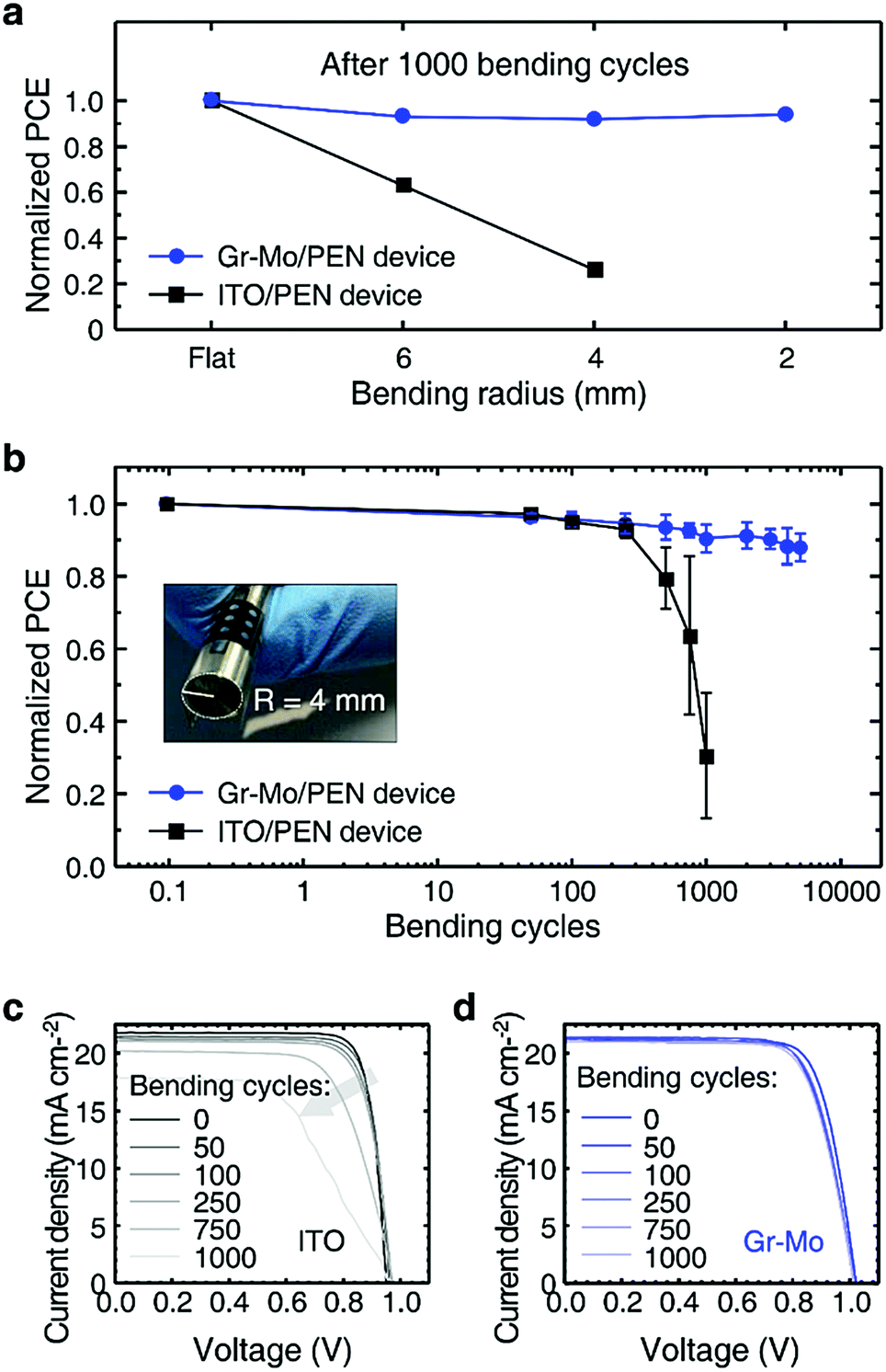 | ||
| Fig. 4 Bending stability test. (a) Normalized PCEs of the Gr-Mo/PEN and ITO/PEN devices measured after 1000 bending cycles with various bending radii: flat, 6, 4, and 2 mm. (b) Normalized PCEs as a function of bending cycles at a fixed bending radius of 4 mm for the Gr-Mo/PEN and ITO/PEN devices. Average values from four separate devices are presented with error bars of standard deviation. The inset photograph shows the Gr-Mo/PEN device bent at a bending radius (R) of 4 mm. (c and d) Evolution of the J–V curves of the (c) ITO/PEN and (d) Gr-Mo/PEN devices throughout 1000 bending cycles with R = 4 mm. | ||
To figure out the origin of PCE degradation in the devices undergoing repeated bending, the morphology of the electrodes and the perovskite films after bending 1000 times were examined using SEM. Fig. 5(a) and (b) show the plane-view SEM images of the ITO/PEN and the Gr-Mo/PEN films, respectively, partially covered with PEDOT:PSS/MAPbI3 layers. When measured after 1000 cycles at R = 4 mm, it was clearly observed, as shown in Fig. 5(a), that a crack was formed on the ITO surface and propagated into the above perovskite film. Therefore, the abrupt decrease in the PCE of the ITO/PEN devices along with bending cycles, shown in Fig. 4(b), could be attributed to the fracture of the brittle ITO films created during repeated bending, which is consistent with the studies reported in previous literatures.6,38 On the other hand, as shown in Fig. 5(b), no cracks were observed either on the graphene surface or on the perovskite surface even under harsh bending conditions (see Fig. S13, ESI†). The failure strain of graphene is known to be ∼25%,39 which is about 25 times larger than that of ITO (∼1%).40 Therefore, graphene could avoid generating cracks under the bending conditions tested in this study, although ITO suffered from crack formation under the same mechanical deformation. Further investigations on the failure of the electrode during bending were undertaken by examining the changes in the relative resistance of the ITO/PEN and Gr-Mo/PEN films as a function of bending cycles at R = 4 mm, as shown in Fig. 5(c). In the case of the ITO/PEN film, the relative change in resistance increased slightly at the beginning, but increased abruptly after 50 bending cycles, reaching 5-fold of the initial value at 1000 bending cycles. On the other hand, in the case of the Gr-Mo/PEN film, the relative change in resistance increased only 0.4-fold from the initial value in total after bending 1000 times. Interestingly, the change in the trend of the resistance for the ITO/PEN film was similar to the PCE reduction trend along with the bending cycles for the ITO/PEN devices, as observed in Fig. 4(b). In addition, in the case of the Gr-Mo/PEN film, regarding the 40% increase in relative resistance during 1000 bending cycles, half of this increase can be attributed to the first 50 bending cycles, and the other half can be attributed to the subsequent 950 bending cycles, which is also similar to the PCE declining trend, shown in Fig. 4(b), of the Gr-Mo/PEN devices along with the bending cycle; regarding the 10% decrease in PCE during 1000 bending cycles, half arose during the first 50 bending cycles, and the other half arose during the following 950 bending cycles. Therefore, the decrease in PCE along with repeated bending may be mainly caused by the resistance increase in the flexible anode electrode. Meanwhile, in the case of the Gr-Mo/PEN electrode, graphene was exceedingly ductile, so the change in the electrical properties due to bending was not so convincing. Another possible factor to increase the relative resistance is the thin metal films formed on graphene as a contact pad for wire-bonding. As shown in Fig. 5(d), when the rectangular Al/Au/Cr metal films formed on the Gr-Mo/PEN substrate as a contact pad were bent twice at R = 4 mm, linear cracks were generated on the films, which could be attributed to the weak adhesion between graphene and the metal surfaces. Therefore, only if provided with a more sufficient contact pad for graphene, flexible devices without any performance degradation due to repeated bending could be realized with a graphene anode.
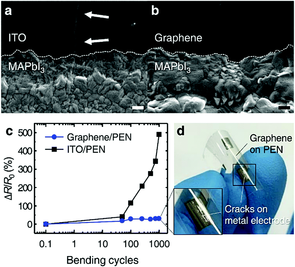 | ||
| Fig. 5 Analysis of performance degradation of the flexible solar cells. (a and b) Plane-view SEM images of the MAPbI3 perovskite films prepared on (a) PEDOT:PSS/ITO/PEN and (b) PEDOT:PSS/Gr-Mo/PEN films, measured after 1000 bending cycles at R = 4 mm (scale bar, 200 nm). (c) Relative resistance change (ΔR/R0) of the Gr-Mo/PEN and ITO/PEN films as a function of bending cycles at R = 4 mm. (d) Photograph of a Gr-Mo/PEN substrate on which rectangular Al/Au/Cr electrodes were formed. When the substrate was bent twice at R = 4 mm, linear cracks were generated on the metal electrodes due to weak adhesion between graphene and the metal surfaces. | ||
Since the Gr-Mo/PEN devices exhibited stable performances showing only 12% degradation in PCE after 5000 bending cycles at R = 4 mm, and only 10% degradation after 1000 cycles at R = 2 mm, a further bending test of up to 5000 cycles at R = 2 mm was carried out to evaluate their potential to be utilized in harsh bending applications. Surprisingly, the Gr-Mo/PEN devices bent as many as 5000 times at R = 2 mm, maintaining a PCE of 85% of its initial value, as shown in (Fig. 6). To the best of our knowledge, this is the first report to demonstrate a stable device operation with a reduction in PCE below 20% after bending 5000 times, at a bending radius of below 4 mm. This result suggests that Gr-Mo/PEN perovskite solar cells have an ultimately high fatigue resistance to become an effective power source to realize future portable and wearable devices.
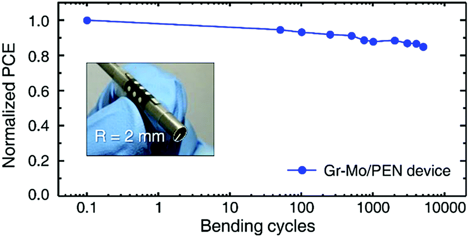 | ||
| Fig. 6 Bending stability test under harsh conditions. The normalized PCE of the Gr-Mo/PEN device as a function of bending cycles with a fixed bending radius, R = 2 mm. | ||
Conclusions
In this work, highly efficient and reliable flexible perovskite solar cells were successfully demonstrated on PEN substrates by utilizing graphene as a transparent conducting anode instead of the typical ITO anode. The currently highest PCE of 16.8%, among TCO-free solar cells, was achieved from the device with no hysteresis. The counterparts fabricated on a flexible ITO electrode also demonstrated a high PCE of 17.3%; however, it decreased significantly to <40% of its initial value after 1000 bending cycles at a bending radius of 4 mm. On the other hand, the devices with graphene electrodes exhibited extremely great bending stabilities, maintaining PCEs of >90% of their original values after 1000 bending cycles, at a bending radius of 2 mm as well as 4 mm. Although the resistance of the graphene electrode was much higher than that of the ITO electrode, the graphene based devices showed higher transmittance, better energy level alignment with the HOMO level of the HTL, larger grains yielding higher JSC and VOC, and a comparable efficiency compared to the ITO-based devices. To estimate the bending stability of the graphene-based devices under harsher bending conditions, the devices were repeatedly bent up to 5000 times at a bending radius of 2 mm, and, surprisingly, their PCEs were maintained at 85% of their initial value even after bending 5000 times. This is, to the best of our knowledge, the first report demonstrating stable device operation with a reduction in PCE below 20% after bending 5000 times at a bending radius of below 4 mm. Neither significant cracks nor an increase in sheet resistance was observed in the Gr-Mo/PEN devices after repeated bending, in contrast to the ITO/PEN devices. This superior robustness against mechanical deformation of the graphene-based perovskite solar cells could enable the realization of foldable photovoltaic devices, exhibiting great potential for new solar device applications.Experimental section
Preparation of flexible substrates with a transparent electrode
For the case of the Gr-Mo/PEN devices, single layer graphene-deposited PEN substrates (Graphene Square Inc., ∼1 kΩ sq−1, 15 × 15 mm2) were obtained using the CVD-grown graphene transfer method and copper foil.41 A CVD-grown single layer graphene film was deposited on the copper foil. PMMA (poly(methyl methacrylate)) was spin-coated on the graphene/copper foil and baked on a hot plate at 180 °C for 1 min and the copper foil was etched using an aqueous solution of ammonium persulfate (H8N2O8S2). Then, the PMMA/graphene sample was transferred on a UV-ozone treated PEN film. The substrate was submerged in acetone solution to remove the PMMA. The resulting graphene/PEN samples were dried using a nitrogen blower. Before device fabrication, Cr (5 nm), Au (50 nm) and Al (100 nm) were consecutively deposited through a rectangular metal aperture mask (2 × 4 mm2) with a vacuum thermal evaporator to provide better electrical contact. To adjust the surface properties of the graphene surface, a 2 nm-thick MoO3 layer was deposited at a rate of 0.1 Å s−1 and annealed at 110 °C for 10 min. For the case of the ITO/PEN devices, ITO/PEN (AMG, 13 Ω sq−1, 25 × 25 mm2) substrates were cleaned with acetone, isopropyl alcohol, and deionized water for 15 min, respectively, followed by UV-ozone treatment for 20 min.Maintaining the flatness of the flexible substrate during the device fabrication process is crucial for realizing highly efficient flexible solar cells. For this, Glass (AMG, 25 × 25 mm2)/PDMS (polydimethylsiloxane) (Dow Corning Sylgard 184) was used as a rigid support. The ITO or graphene/PEN substrate was attached on the support during the whole fabrication process. After this, the complete device was peeled off from the support to be characterized.
Fabrication of perovskite solar cells
A filtered PEDOT:PSS (Clevios P VP Al 4083, Heraeus)/deionized water (2![[thin space (1/6-em)]](https://www.rsc.org/images/entities/char_2009.gif) :1 v/v) solution was spin-coated on the prepared substrate at 5000 rpm for 40 s and dried at 110 °C for 30 min. Then, the MAPbI3 perovskite layer was fabricated via a Lewis base adduct method.32 A precursor solution was prepared by dissolving PbI2 (Alfa Aesar)/MAI (synthesized using a previously reported method3)/DMSO (Sigma Aldrich) (1:1:1 molar ratio) into DMF (Sigma Aldrich) at 50 wt%. 30 μL of the solution was spin-coated at 4000 rpm for 20 s and 0.3 mL of diethyl ether (Sigma Aldrich) was casted for 8 s after initiating spin-coating. Then a yellow, transparent perovskite layer of the intermediate phase was formed and changed into dark, brown-colored MAPbI3 during a two-step annealing process at 65 °C for 1 min and at 100 °C for 4 min. All of the spin-coating processes were conducted at a relative humidity of <20% and a temperature of 25 °C. Deposition of C60 (20 nm), BCP (10 nm), LiF (0.5 nm) and Al (150 nm) was conducted using a vacuum thermal evaporator under a pressure of ∼10−7 bar.
:1 v/v) solution was spin-coated on the prepared substrate at 5000 rpm for 40 s and dried at 110 °C for 30 min. Then, the MAPbI3 perovskite layer was fabricated via a Lewis base adduct method.32 A precursor solution was prepared by dissolving PbI2 (Alfa Aesar)/MAI (synthesized using a previously reported method3)/DMSO (Sigma Aldrich) (1:1:1 molar ratio) into DMF (Sigma Aldrich) at 50 wt%. 30 μL of the solution was spin-coated at 4000 rpm for 20 s and 0.3 mL of diethyl ether (Sigma Aldrich) was casted for 8 s after initiating spin-coating. Then a yellow, transparent perovskite layer of the intermediate phase was formed and changed into dark, brown-colored MAPbI3 during a two-step annealing process at 65 °C for 1 min and at 100 °C for 4 min. All of the spin-coating processes were conducted at a relative humidity of <20% and a temperature of 25 °C. Deposition of C60 (20 nm), BCP (10 nm), LiF (0.5 nm) and Al (150 nm) was conducted using a vacuum thermal evaporator under a pressure of ∼10−7 bar.
Characterization
J–V curves of the perovskite solar cells were measured using a source meter (Keithley 2400, Tektronix) under 100 mW cm−2, AM 1.5G simulated one-sun illumination using a solar simulator (Sol 3A Class AAA 64023A, Oriel) with calibration using the KG-5 standard Si-cell. Step voltage and delay time for the forward and reverse scan were set to 20 mV and 200 ms, respectively. Each device was covered with a metal aperture mask to set the active area to 1.77 mm2. EQE spectra were measured using a quantum efficiency measurement system (IQE-200B, Oriel) equipped with a 100 mW Xenon lamp and an amplifier. To estimate the mechanical durability of the flexible solar cells, each device was repeatedly bent at a frequency of 1 Hz using a bending test machine (1Axis, Science Town). EIS measurements were implemented using an electrochemical potentiostat (CHI 600D, CH Instruments). The measurements mentioned above were carried out inside a nitrogen-filled glove box. Transmittance spectra were obtained using a UV-visible spectrophotometer (Cary 5000, Agilent technologies). Plane-view SEM images were obtained using field-emission scanning electron microscopy (AURIGA, Carl Zeiss) and cross-sectional SEM images were obtained using a focused-ion-beam (FIB) system (AURIGA, Carl Zeiss). The surface roughness profile was measured using atomic force microscopy (NX10, Park Systems) in the noncontact mode. The UPS spectra of the transparent electrodes were measured using an Axis-Nova (Kratos) with a He discharge lamp. X-ray diffraction analysis was implemented to characterize the crystal structure using a New D8 Advance (Bruker). All of the tests were conducted at room temperature.Acknowledgements
This work was financially supported by the Global Frontier R&D Program of the Center for Multiscale Energy System (2012M3A6A7054855). The work was also supported by the National Research Foundation of Korea (NRF), funded by the Ministry of Education, Science and Technology (NRF-2014R1A4A1008474).Notes and references
- A. Kojima, K. Teshima, Y. Shirai and T. Miyasaka, J. Am. Chem. Soc., 2009, 131, 6050–6051 CrossRef CAS PubMed.
- J.-H. Im, C.-R. Lee, J.-W. Lee, S.-W. Park and N.-G. Park, Nanoscale, 2011, 3, 4088–4093 RSC.
- H.-S. Kim, C.-R. Lee, J.-H. Im, K.-B. Lee, T. Moehl, A. Marchioro, S.-J. Moon, R. Humphry-Baker, J.-H. Yum, J. E. Moser, M. Grätzel and N.-G. Park, Sci. Rep., 2012, 2, 591 Search PubMed.
- M. M. Lee, J. Teuscher, T. Miyasaka, T. N. Murakami and H. J. Snaith, Science, 2012, 338, 643–647 CrossRef CAS PubMed.
- W. S. Yang, J. H. Noh, N. J. Jeon, Y. C. Kim, S. Ryu, J. Seo and S. I. Seok, Science, 2015, 348, 1234–1237 CrossRef CAS PubMed.
- B. J. Kim, D. H. Kim, Y.-Y. Lee, H.-W. Shin, G. S. Han, J. S. Hong, K. Mahmood, T. K. Ahn, Y.-C. Joo, K. S. Hong, N.-G. Park, S. Lee and H. S. Jung, Energy Environ. Sci., 2015, 8, 916–921 CAS.
- Y. Li, L. Meng, Y. M. Yang, G. Xu, Z. Hong, Q. Chen, J. You, G. Li, Y. Yang and Y. Li, Nat. Commun., 2016, 7, 10214 CrossRef CAS PubMed.
- J. H. Heo, S. H. Im, J. H. Noh, T. N. Mandal, C.-S. Lim, J. A. Chang, Y. H. Lee, H.-J. Kim, A. Sarkar, M. K. Nazeeruddin, M. Grätzel and S. I. Seok, Nat. Photonics, 2013, 7, 486–491 CrossRef CAS.
- D. Liu and T. L. Kelly, Nat. Photonics, 2014, 8, 133–138 CrossRef CAS.
- D. Yang, R. Yang, J. Zhang, Z. Yang, S. F. Liu and C. Li, Energy Environ. Sci., 2015, 8, 3208–3214 CAS.
- J. M. Ball, M. M. Lee, A. Hey and H. J. Snaith, Energy Environ. Sci., 2013, 6, 1739–1743 CAS.
- J. You, Z. Hong, Y. M. Yang, Q. Chen, M. Cai, T.-B. Song, C.-C. Chen, S. Lu, Y. Liu, H. Zhou and Y. Yang, ACS Nano, 2014, 8, 1674–1680 CrossRef CAS PubMed.
- P. Docampo, J. M. Ball, M. Darwich, G. E. Eperon and H. J. Snaith, Nat. Commun., 2013, 4, 2761 Search PubMed.
- S. Das, B. Yang, G. Gu, P. C. Joshi, I. N. Ivanov, C. M. Rouleau, T. Aytug, D. B. Geohegan and K. Xiao, ACS Photonics, 2015, 2, 680–686 CrossRef CAS.
- C. Roldán-Carmona, O. Malinkiewicz, A. Soriano, G. M. Espallargas, A. Garcia, P. Reinecke, T. Kroyer, M. I. Dar, M. K. Nazeeruddin and H. J. Bolink, Energy Environ. Sci., 2014, 7, 994–997 Search PubMed.
- I. Jeon, T. Chiba, C. Delacou, Y. Guo, A. Kaskela, O. Reynaud, E. I. Kauppinen, S. Maruyama and Y. Matsuo, Nano Lett., 2015, 15, 6665–6671 CrossRef CAS PubMed.
- K. Sun, P. Li, Y. Xia, J. Chang and J. Ouyang, ACS Appl. Mater. Interfaces, 2015, 7, 15314–15320 CAS.
- S. S. Shin, W. S. Yang, E. J. Yeom, S. J. Lee, N. J. Jeon, Y.-C. Joo, I. J. Park, J. H. Noh and S. I. Seok, J. Phys. Chem. Lett., 2016, 7, 1845–1851 CrossRef CAS PubMed.
- D. Yang, R. Yang, X. Ren, X. Zhu, Z. Yang, C. Li and S. F. Liu, Adv. Mater., 2016, 28, 5206–5213 CrossRef CAS PubMed.
- C. Wang, D. Zhao, C. R. Grice, W. Liao, Y. Yu, A. Cimaroli, N. Shrestha, P. J. Roland, J. Chen, Z. Yu, P. Liu, N. Cheng, R. J. Ellingson, X. Zhao and Y. Yan, J. Mater. Chem. A, 2016, 4, 12080–12087 CAS.
- H. Yoon, S. M. Kang, J.-K. Lee and M. Choi, Energy Environ. Sci., 2016, 9, 2262–2266 CAS.
- X. Li, Y. Zhu, W. Cai, M. Borysiak, B. Han, D. Chen, R. D. Piner, L. Colombo and R. S. Ruoff, Nano Lett., 2009, 9, 4359–4363 CrossRef CAS PubMed.
- K. K. Kim, A. Reina, Y. Shi, H. Park, L.-J. Li, Y. H. Lee and J. Kong, Nanotechnology, 2010, 21, 285205 CrossRef PubMed.
- S. Bae, H. Kim, Y. Lee, X. Xu, J.-S. Park, Y. Zheng, J. Balakrishnan, T. Lei, H. R. Kim, Y. I. Song, Y.-J. Kim, K. S. Kim, B. Özyilmaz, J.-H. Ahn, B. H. Hong and S. Iijima, Nat. Nanotechnol., 2010, 5, 574–578 CrossRef CAS PubMed.
- A. R. Bin Mohd Yusoff, D. Kim, F. K. Schneider, W. J. da Silva and J. Jang, Energy Environ. Sci., 2015, 8, 1523–1537 Search PubMed.
- H. Sung, N. Ahn, M. S. Jang, J.-K. Lee, H. Yoon, N.-G. Park and M. Choi, Adv. Energy Mater., 2016, 6, 1501873 CrossRef.
- J.-K. Lee, H. Sung, M. S. Jang, H. Yoon and M. Choi, J. Mater. Chem. C, 2015, 3, 8294–8299 RSC.
- H. Liu, Y. Liu and D. Zhu, J. Mater. Chem., 2011, 21, 3335–3345 RSC.
- W. Chen, S. Chen, D. C. Qi, X. Y. Gao and A. T. S. Wee, J. Am. Chem. Soc., 2007, 129, 10418–10422 CrossRef CAS PubMed.
- O. Leenaerts, B. Partoens and F. Peeters, Phys. Rev. B: Condens. Matter Mater. Phys., 2008, 77, 125416 CrossRef.
- Z. Chen, I. Santoso, R. Wang, L. F. Xie, H. Y. Mao, H. Huang, Y. Z. Wang, X. Y. Gao, Z. K. Chen, D. Ma, A. T. S. Wee and W. Chen, Appl. Phys. Lett., 2010, 96, 213104 CrossRef.
- N. Ahn, D.-Y. Son, I.-H. Jang, S. M. Kang, M. Choi and N.-G. Park, J. Am. Chem. Soc., 2015, 137, 8696–8699 CrossRef CAS PubMed.
- J. Seo, S. Park, Y. C. Kim, N. J. Jeon, J. H. Noh, S. C. Yoon and S. I. Seok, Energy Environ. Sci., 2014, 7, 2642–2646 CAS.
- J. H. Heo, H. J. Han, D. Kim, T. K. Ahn and S. H. Im, Energy Environ. Sci., 2015, 8, 1602–1608 CAS.
- E. J. Juarez-Perez, M. Wußler, F. Fabregat-Santiago, K. Lakus-Wollny, E. Mankel, T. Mayer, W. Jaegermann and I. Mora-Sero, J. Phys. Chem. Lett., 2014, 5, 680–685 CrossRef CAS PubMed.
- Q. Dong, Y. Yuan, Y. Shao, Y. Fang, Q. Wang and J. Huang, Energy Environ. Sci., 2015, 8, 2464–2470 CAS.
- J. H. Heo, M. H. Lee, H. J. Han, B. R. Patil, J. S. Yu and S. H. Im, J. Mater. Chem. A, 2016, 4, 1572–1578 CAS.
- J. W. Jo, M.-S. Seo, M. Park, J.-Y. Kim, J. S. Park, I. K. Han, H. Ahn, J. W. Jung, B.-H. Sohn, M. J. Ko and H. J. Son, Adv. Funct. Mater., 2016, 26, 4464–4471 CrossRef CAS.
- C. Lee, X. Wei, J. W. Kysar and J. Hone, Science, 2008, 321, 385–388 CrossRef CAS PubMed.
- Z. Chen, B. Cotterell and W. Wang, Eng. Fract. Mech., 2002, 69, 597–603 CrossRef.
- W. H. Lee, J. Park, S. H. Sim, S. B. Jo, K. S. Kim, B. H. Hong and K. Cho, Adv. Mater., 2011, 23, 1752–1756 CrossRef CAS PubMed.
Footnotes |
| † Electronic supplementary information (ESI) available. See DOI: 10.1039/c6ee02650h |
| ‡ These authors contributed equally to this work. |
| This journal is © The Royal Society of Chemistry 2017 |