
Self-assembled monolayers in organic electronics
Stefano
Casalini†
a,
Carlo Augusto
Bortolotti
 ab,
Francesca
Leonardi†
c and
Fabio
Biscarini
*ac
ab,
Francesca
Leonardi†
c and
Fabio
Biscarini
*ac
aLife Sciences Department, University of Modena and Reggio Emilia, Via Campi 103, 41125 Modena, Italy. E-mail: fabio.biscarini@unimore.it
bConsiglio Nazionale delle Ricerche (CNR), Institute for Nanosciences, Via Campi 213/a, 41125 Modena, Italy
cConsiglio Nazionale delle Ricerche (CNR), Institute for Nanostructured Materials (ISMN), Via P. Gobetti 101, 40129 Bologna, Italy
First published on 7th October 2016
Abstract
Self-assembly is possibly the most effective and versatile strategy for surface functionalization. Self-assembled monolayers (SAMs) can be formed on (semi-)conductor and dielectric surfaces, and have been used in a variety of technological applications. This work aims to review the strategy behind the design and use of self-assembled monolayers in organic electronics, discuss the mechanism of interaction of SAMs in a microscopic device, and highlight the applications emerging from the integration of SAMs in an organic device. The possibility of performing surface chemistry tailoring with SAMs constitutes a versatile approach towards the tuning of the electronic and morphological properties of the interfaces relevant to the response of an organic electronic device. Functionalisation with SAMs is important not only for imparting stability to the device or enhancing its performance, as sought at the early stages of development of this field. SAM-functionalised organic devices give rise to completely new types of behavior that open unprecedented applications, such as ultra-sensitive label-free biosensors and SAM/organic transistors that can be used as robust experimental gauges for studying charge tunneling across SAMs.
 Stefano Casalini | Stefano Casalini received his PhD in Chemistry at the University of Modena and Reggio Emilia in 2008 working on amperometric biosensors. He has been collaborating with industry (Tetrapak s.p.a.) before joining the Italian National Research Council in 2009, where he worked in the field of Molecular Electronics and BioElectronics. He was actively involved as a task leader in two European projects: (i) “Organic Nanomaterials for Electronics and Photonics” and (ii) “Implantable Organic Nano-Electronics”. He is actually a TECNIOSpring 2015 fellow co-funded by EU commission through FP7 Marie Curie Actions at the Insitut de Ciència de Materials de Barcelona. |
 Carlo Augusto Bortolotti | Carlo Augusto Bortolotti is an Assistant Professor of Physical Chemistry at the University of Modena and Reggio Emilia. He received his PhD in Chemistry in 2006; from 2006 to 2008 he was a PostDoc at the S3 Centre (now Institute Nanoscience) of the Italian National Research Council (CNR). He has been a visiting fellow at the Technical University of Denmark DTU, University College London UCL, Brandeis University. His main research interests concern the combined experimental and computational design and production of bio-(in)organic interfaces for nanobiotechnological applications. |
 Francesca Leonardi | Francesca Leonardi received her PhD in Chemistry at the “Alma Mater Studiorum” University of Bologna in 2014. Her main topic was the extensive use of organic transistors as molecular gauges for the study of charge injection in self-assembled monolayers. Afterwards, she joined the research group of Dr V. Palermo whose objective was focused on developing new strategies for graphene functionalization. In 2015, she moved to the Institut de Ciència de Materials de Barcelona in order to develop a new sensing platform in the field of Organic Electronics as a “Juan de la Cierva” post doc fellow. She is co-author of more than 16 peer-reviewed papers. |
 Fabio Biscarini | Fabio Biscarini is a Full Professor of General Chemistry at the University of Modena and Reggio Emilia. He received the PhD degree in Chemistry from the University of Oregon, USA, in 1993. He is a Fellow of the Royal Society of Chemistry, and a recipient of 2012 Premio Sapio for Industrial Research 2012 and 2007 EU-Descartes Prize 2007. His research spanned the theory of STM, thin film growth phenomena, self-organization, and unconventional nanofabrication. His current interests are on fundamental aspects of organic field effect transistors and on organic bioelectronics, with focus on biosensors and implantable devices for regenerative treatment of spinal cord injury and Parkinson's disease. |
Introduction
We review the applications of self-assembled monolayers (SAMs) in organic electronics. Since the first report of SAM-functionalized electrodes for controlling the contact resistance in organic field effect transistors,1 the use of SAMs on electrodes, dielectrics, and semiconductors has become a widely adopted and versatile approach for modulating the interfacial properties of organic electronic devices. SAMs enhance the stability and the response of organic electronic devices; they also enable the design of new experiments and device layouts, leading to new physical–chemical insights into the phenomena governing the device response. SAM-functionalised organic devices have ultimately bridged the gap between molecular and organic electronics.We hope to convey the reader that SAMs on technology-relevant interfaces for organic electronics lead to new and exciting developments, especially in emerging areas like biosensors and nanomedicine. We are confident that both the specialist of the field and the broader readership with an interest in the fundamental aspects of self-assembly will find this review useful and/or inspiring.
1. Brief overview on principles and applications of SAMs
1.1 Universal aspects of self-assembly
According to Whitesides and Grzybowski, “self-assembly is the autonomous organization of components into patterns and structures, without human intervention”.2 Self-assembly is a unifying concept in nature.3 The origin of many systems, both living and unanimated, that exhibit characteristic length scales larger than the ones of their individual components, can be re-conducted to self-assembly. It leads to the formation of hierarchically complex structures with spatial correlations across multiple length-scales.Restricting the definition to molecular self-assembly, the key ingredient is the coexistence of covalent (hard) and non-covalent (soft) interactions with different length scales and comparable energy contributions. Non-covalent interactions relevant to self-assembly include: hydrogen bonding, electrostatic interactions, hydrophobic interactions, steric repulsion, van der Waals forces3 (Fig. 1). Nature builds complex systems by assembling them piecewise3 starting from a relatively limited number of building blocks: amino acids, nucleotides, lipids and sugars. Relevant examples of self-assembly in nature include the formation of micelles and bilayers from amphiphilic molecules, the folding and aggregation of peptides and proteins, the structure of nucleic acids and their complexes with proteins, cellular membranes, bio-molecular machines and motors, and scaffolds (Fig. 1).
 | ||
| Fig. 1 Top: Non-covalent interactions underlying self-assembly. Bottom: Cartoon representation of some of the most-relevant examples of naturally-occurring hierarchical structures. | ||
The potential of exploiting the recognition properties of chemically-designed building units has inspired scientists to pursue the bottom-up construction of functional assemblies and complex machinery. If, on one hand, molecular design allows chemists to program self-assembled building blocks, on the other hand the dynamics of self-assembly is not always amenable for the strict control demanded by technology. Difficulty in governing the competing dynamic processes has hampered the bottom-up fabrication to become technology-viable for the integration of nanostructures into devices with addressable functions.
1.2 Characteristics of SAMs
SAMs represent a success story of a robust and versatile approach to fine-tune a surface of interest. A systematic investigation of the self-organization of molecules from the solution phase to a surface was first reported in 1946,4,5 although the fortunate definition of such constructs as “self-assembled monolayers” came nearly twenty years later by J. Sagiv6 and proposed as for applications by G. M. Whitesides and coworkers.7SAM formation requires chemisorption on a surface followed by the spontaneous organization into 2D-crystalline long-range molecularly ordered domains.8–10 The molecules amenable for SAMs are typically composed of three parts: (i) the head group, that is the end of the molecule which binds to the surface, (ii) a backbone made of an aliphatic chain and/or an aromatic oligomer, mostly responsible for the molecular ordering, and (iii) the terminal group, which determines topography,6 surface energy,11 and chemistry6 of the outer interface (Fig. 2). Albeit this convention is the most widely adopted one, it is quite common to find papers where the terminal group is termed as the head one.
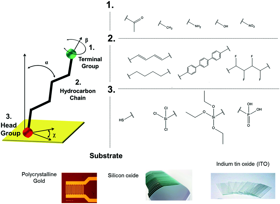 | ||
| Fig. 2 Top: On the left, sketch of a typical aliphatic self-assembling molecule: the three major components (head, backbone and tail) are highlighted; on the right, some of the most common terminal groups and backbone for self-assembly. Adapted from ref. 25 with permission from The Royal Society of Chemistry. Bottom: Some of the extensively used substrates for functionalization via self-assembly. | ||
Self-assembly on a surface results from the interplay of (i) the affinity of the head group for the surface, which imparts the orientation of the adlayer and templates the structure in the case of crystalline surfaces, (ii) the non-covalent lateral interactions between the chains, that stabilize the structure and yield molecular order, and (iii) the intramolecular interactions which determine the fine details of the super-lattice structure (e.g. tilt-angle, surface lattice reconstruction). An important feature of SAMs is their dynamic behaviour, including conformational isomerism, lateral diffusion and reconstruction in response to environmental conditions.10,12,13 The softness of the non-covalent interactions translates into low energy kinetic barriers that allow the molecules to attain the minimum free energy configuration in the SAM even at room temperature and despite the reduced number of degrees of freedom experienced within a molecularly dense phase on a surface-restricted space. A balance between hard and soft interactions is also important for overcoming the presence of defects on the underlying surface, reducing or annihilating them in the SAM. Relevant examples are ordered SAMs on amorphous surfaces formed by alkylphosphonates on metal oxides or alkylsilanes on hydroxylated silicon oxide.14 In turn, mismatched energy of covalent and non-covalent interactions as well as excessive chain rigidity can lead to disordered metastable SAM phases. These arguments highlight the importance of molecular design also to control the kinetics of SAM formation.
For the above reasons, SAM surface functionalisation is convenient for defining the chemistry of surfaces that are far from ideal, like the technological surfaces that are either polycrystalline or amorphous, often exposed to ambient contamination (SAM molecules will “clean” out physisorbed and even strongly adsorbed contaminants), or processed and used in environments less controlled than ultra-high vacuum conditions.11
1.3 Examples of SAMs
SAMs can be formed from molecules either dissolved in solution or condensing on the surface from a gas phase.15 Although the vast majority of examples concern solid (poly-)crystalline surfaces, SAMs also form on liquid surfaces such as alkanethiol SAMs on mercury drops.16 These have been demonstrated as the most effective top electrodes for making reproducible vertical molecular junctions in the investigation of tunnelling and charge transfer across SAMs.17,18 SAMs on liquid surfaces can be viewed as an intermediate case between the chemisorbed SAMs on crystalline solids and Langmuir films, where molecules are weakly physisorbed on a liquid surface.8If the head and terminal groups are identical or exhibit chemical affinity, SAMs give rise to multilayer structures. Examples are alkane dithiols forming disulphide bonds, or silanol head groups interacting with carboxylic terminal groups as in constructive lithography.19 The layer-by-layer controlled growth process may face the competition of dual binding that leads to the molecules flat-lying on the substrate as opposed to homeotropic orientation.20 This is especially relevant for short and rigid chain lengths, else for very-long and flexible chains, where the coexistence of standing domains with a more disordered planar phase prevents the formation of a continuous SAM.8
The two prototypical SAMs are alkanethiols on Au(111)10,11,21–25 and organo-silicon monolayers on hydroxylated silicon oxide surfaces.6,9,14,20 In the context of organic electronics, the former might be regarded as a model for SAM-functionalized polycrystalline Au electrodes, and the latter as a model for a SAM-functionalized channel of a planar device.24
Monolayers of n-alkanethiols on gold are easy to prepare and yield highly ordered and large 2D crystalline domains. They have become a paradigmatic system for understanding and fine-tuning the morphology and the functionality of SAM-based systems.8,10 Due to the increased availability of tools for nanoscale characterization, insights into the mechanisms leading to SAM formation and into the correlation between their structure and properties have been gained. It is nowadays accepted that a “lying-down” kinetic phase at low surface coverage precedes the formation of a “standing-up” phase with two-dimensional long-range order, the latter occurring at a surface coverage higher than a critical value.8,10,12,26 Parameters controlling self-assembly include temperature, chain length and nature, concentration of the SAM-forming molecules and their solvent, the incubation time and the preparation of the substrate surface.10
SAMs can be formed also with aromatic backbone chains27–30 and on a variety of metal substrates (Pd,31 Ag(111)32,33 and Cu(111)34–38). Interestingly, alkanethiols with chains shorter than 10 units do not form a SAM on Au, rather a highly defective monolayer or, in the case of very short chains, a 2D disordered phase (2D gas or liquid) with molecules diffusing across the surface.39
Organo-silicon monolayers are formed by condensation on substrates exposing hydroxyl groups like silicon oxide SiO2 grown on silicon substrates,14 quartz,40 Al2O321,22,26 and ITO (tin-doped indium oxide).41–45 Although these systems gained lesser attention as “archetypal”8 cases for fundamental aspects of self-assembly, they represent technological and industry-relevant systems where functional properties and processing steps are tuned by means of the grafting layer. The most investigated systems are alkyltrichlorosilanes, especially octadecyltrichlorosilanes (ODTSs, CH3–(CH2)17–SiCl3), which are usually believed to irreversibly graft both to the surface and to the neighbouring SAM molecules by a siloxane Si–O–Si bonding network. From a morphological point of view, siloxane-based SAMs do not exhibit a crystalline structure9,46 and they display a smaller tilt angle and correlation length with respect to thiols on Au. Moreover, due to the extensive binding of the head groups to the surface via strong and localized bonds, and to the partial in-plane cross-linking between adjacent molecules, siloxane-based SAMs are less mobile and hence less prone to structural rearrangements upon annealing, in comparison with thiol–Au systems.9 Annealing is a processing step widely used in the fabrication of organic electronic devices, and hence this approach is viable for defining the surface chemistry of oxides in a range of temperatures.
Besides organo-silicon monolayers, organo-phosphonates featuring both aliphatic or aromatic chains have been grafted on the native oxide surface of Si,47 ITO,48 Ti43,44 and titanium alloys.49 When compared to siloxane-based films, organo-phosphonate SAMs exhibit a higher degree of order and are more durable.43,50 They form homogeneous SAMs that adhere strongly to the substrate.51 Their high resistance to moisture and the possibility of forming them under ambient conditions, together with their great versatility, make these SAMs attractive candidates for several industrial applications where the systems are exposed to water.
1.4 Applications of SAMs outside oganic electronics
The possibility of controlling the immobilization of a protein on a substrate has been extensively investigated (Fig. 3).52,55,56 This is important in bioelectronics,57 which is based on the tethering of a biomolecule to a (semi-)conductive substrate and the transduction of recognition events into a potential or a current change.55 One of the trickiest aspects concerning the design of bioactive interfaces is the retention of the protein functionality upon surface adsorption. To this end, functionalization of the electrode substrate with SAMs prior to biomolecule adsorption represents a viable route to avoid protein denaturation at the surface.58
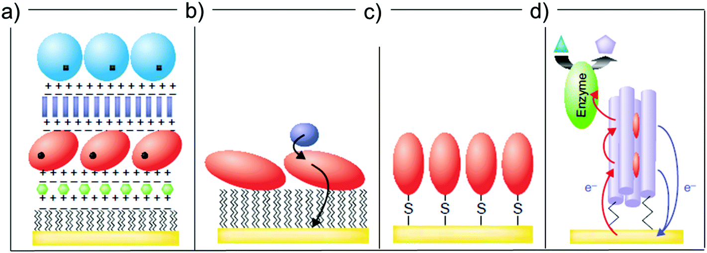 | ||
| Fig. 3 Different strategies of protein (red globule) immobilization: (a) electrostatic layer-by-layer, (b) hydrophobic physisorption onto a SAM, (c) direct covalent link, (d) covalent tethering through a SAM. Reproduced with permission from ref. 52. Copyright © 2001 Elsevier Science Ltd. All rights reserved. | ||
Once a SAM is formed on the substrate, proteins can be immobilized atop in two ways. The first one is by physisorption via electrostatic interaction between the terminal groups of the SAM-forming molecules and the protein itself (Fig. 3a),59–62 or via the hydrophobic interaction between low-energy surfaces (typically –CH3 terminated SAMs) and the apolar patch of the biomolecule of interest (Fig. 3b).63,64
A second strategy concerns the immobilization of the protein via formation of chemical bond(s) between the terminal group of the SAM and one or more surface exposed protein aminoacid side chains (chemisorption, as shown in Fig. 3c). Covalent binding leads to a more robust bio-interface and, very importantly, can be used to achieve a controlled orientation of the protein with respect to the surface, thus enhancing its electrical communication with the surface (Fig. 3d). Several bioconjugation techniques have been employed to covalently bind a protein to a SAM: one of the most used is N-ethyl-N′-(3-dimethylaminopropyl) carbodiimide (EDC)/N-hydroxysuccinimide (NHS) coupling, which enables for the activation of carboxylate terminal groups in the SAM to bind surface-exposed primary amines of the protein.65
As previously stated, SAMs can be used to avoid binding of biological species (proteins but also living organisms) to a substrate, a phenomenon termed fouling. Inertness towards protein adsorption is an important requirement for biocompatible materials.66–68 In order to be a suitable candidate for applications as contact lenses,69 implantable devices, prostheses, and catheters, the material must prevent the adsorption of proteins.70,71 The same stands for cell cultures,72 tissue engineering,73 drug delivery74 and microfluidics.75
In a number of biotechnological applications, the engineering of a bio/inorganic interface able to selectively bind the biological target is central. The material must be anti-fouling with respect to all biological species except for the one of interest, typically the target analyte to be quantified in a complex biological sample. Poly(ethylene glycol), PEG, has been widely used as a coating material for biomedical applications to avoid protein adsorption. Since the early 1990s, SAMs have been thoroughly tested as grafted layers to endow surfaces with antifouling properties comparable or even superior to those of PEG. The first attempts were aimed at mimicking PEG-derivatized substrates by using monolayers with 3–6 ethylene glycol units within the terminal group of the SAM-forming molecules, viz. –(EG)3OH and –(EG)6OH.76–78 Chapman et al.79 screened more than 50 surfaces functionalized with different SAMs for their ability to resist protein adsorption. Their results allowed them to list four molecular features for a SAM-modified surface to be antifouling:66,79,80 (i) the SAM should be hydrophilic; (ii) it must contain hydrogen-bond acceptors, but (iii) not include hydrogen-bond donors and (iv) its overall electrical charge should be neutral. Besides proteins, oligo-(ethylene glycol) (OEG)-terminated SAMs were demonstrated to be fouling resistant also to cells, both eukaryotic81–83 and bacterial.84
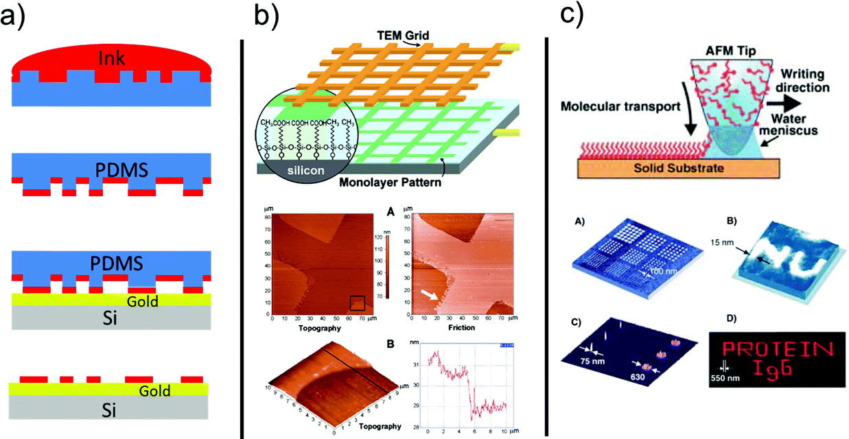 | ||
| Fig. 4 (a) Stepwise process of micro-contact printing. Adapted from ref. 86. Copyright © 2016 Elsevier Science Ltd. All rights reserved. (b) Constructive lithography by using a TEM grid. (c) Dip-pen nanolithography. Reproduced with permission from ref. 19 (Copyright © 2003, American Chemical Society) and ref. 90 (Copyright © 2004 Wiley-VCH Verlag GmbH & Co. KGaA, Weinheim). | ||
Micro-contact printing relies on a polydimethylsiloxane (PDMS) stamp imbibed with SAM-forming molecules from an alcoholic solution. When the stamp is contacted to an Au film on a substrate, the SAM is formed in a short time at the regions of intimate contact between the stamp and the substrate. The result is the positive transfer of the stamp pattern to the surface.86,87
In constructive lithography, the terminal group of a SAM on native silicon is patterned by means of a conductive tip of an AFM or using a conductive stamp. The SAM terminal group is modified by flowing a current across the stamp/SAM/silicon junction. Either a local anodic oxidation or a cathodic reduction can be exploited depending on the nature of the terminal group.19,88,91 A second molecular layer, else a metal precursor, can be precisely adsorbed on top of the modified regions by preferential interactions.
DPN is a local implementation derived from the success of micro-contact printing. The AFM tip is coated with SAM-forming molecules which are then released to the substrate by diffusion of the molecules through the water meniscus formed between the probe and the substrate.90,92,93
Other SAM patterning approaches, such as nanoshaving94,95 and nanografting,96 are versatile techniques to create small-area patterns of nano-sized structures with functionality different from the SAM matrix. They have been used to create templates for the adsorption of a controlled number of biomolecules (like DNA triplex- and quadruplex) or for the positioning of single-walled carbon nanotubes (SWNTs) on surfaces.97
P. Weiss has studied the self-organised morphology of phase-segregated SAM-blends.98 The extension from planar metal surfaces to curved ones of binary SAMs with competing interactions has led to intriguing patterns reported on curved surfaces, such as those of nanoparticles.99,100 The possibility of creating a SAM shell where surface tension and chemical reactivity can be modulated on the nanometer length scales opens interesting perspectives in fields ranging from drug delivery to cells, to chemical reactivity.13,101
In conclusion, SAMs represent the paradigm of bottom-up nanotechnology for their capability to build up architectures integrated at multiple length scales. They are versatile because of their modular design and ease of processing. They are robust nanoscale systems for applications where the tailoring of interfacial properties of objects of all sizes is central.10
2. SAM-modified organic field effect transistors
Organic electronics exploits charge transport across thin films of π-conjugated polymers and molecules connecting the electrodes of a solid-state device. The organic field effect transistor (OFET) is the central device for the development of digital logic circuits and memories. They are also emerging as ultra-sensitive sensors, biosensors and bio-transducers.102,103In OFETs, the organic semiconductor (OSC) thin film forms the channel between source and drain electrodes. A dielectric thin film separates the channel from the gate electrode whose voltage modulates the charge carrier density.104 Test devices patterned on silicon oxide (as gate dielectric)/highly-doped p-silicon wafer (as gate) are often used to characterize the charge transport in OSCs.105,106 From the I–V characteristics, charge mobility (μ) can be extracted and the level of adventitious dopants can be estimated from the threshold voltage (Vth) and the on–off ratio.107 However, the measured properties are very sensitive to the nature of the device interfaces, such as OSC/gate dielectric and OSC/electrode.108,109 This should be kept in mind while the aim is to establish the correlation between the charge transport properties and molecular design, structure and ordering in the thin film. This is discussed below.
2.1 OSC/gate dielectric interface
OFETs are low-dimensional devices, where the charge carriers are accumulated in the channel within a few nanometers (viz. the equivalent of 1–3 molecular layers) from the gate dielectric.110–112 The charge mobility and threshold voltage are extremely sensitive to the surface chemistry of the gate dielectric.The presence of charged (pH-dependent) and redox reactive sites at the gate dielectric affects the density of charge carriers.113 The gate chemical potential sets the threshold voltage in the thin film. The reactivity of the dielectric/organic interface is responsible for the phenomenon termed bias stress, which results in the Vth shift upon repeated OFET operations with the decay of the source–drain current. The recovery of OFET characteristics upon reverse-gate bias suggests that the reaction is reversible, thus the reactive sites act as shallow traps for carriers. Within this respect, SAM formation may reduce or modify surface reactivity.114
The surface chemistry of the gate dielectric is also crucial in determining the molecular order and thin film morphology.115,116 The OSC films are deposited on the device under non-equilibrium conditions. Therefore, thin film morphology is the result of non-equilibrium phenomena such as nucleation, growth, dewetting, ripening, and recrystallization occurring at the interface between the organic semiconductor and the dielectric. The molecules experience energy barriers associated with kinetic steps (like diffusion, aggregation, and desorption) that are affected by the dielectric surface tension and roughness. The interplay of these kinetic steps with the flux of molecules from the fluid phase (liquid, solution or gas) selects the dominant kinetic process.117 SAM formation affects surface tension and roughness, and hence the mechanism of growth.118,119
The dielectric surface will also affect the crystal OSC structure.120 First, surface tension biases the orientation of different crystalline facets during nucleation. Molecular orientation with respect to the channel is crucial, as charge mobility is usually anisotropic in π-conjugated materials. Second, it will change the critical size and the dimensionality of nuclei. Third, it selects one of the co-existing OSC polymorphs thus establishing the intermolecular hopping of the charge carriers through the molecular packing and overlap integral. It is important to select the one with the highest overlap. SAM formation affects the surface tension and hence the structure.
2.2 OSC/electrode interface
The source (drain) electrode–semiconductor interface controls charge injection and the morphology of the thin film on electrodes.121 Charge injection depends on the electronic structure of the interface. The latter is completely different from the morphology on the channel, because metal electrodes exhibit a topographical relief and edge discontinuity, roughness, and a granular structure that are much more relevant with respect to those of the gate dielectric. The interaction of metal surfaces with π-conjugated species is strong, due to image potential and polarisation effects. The diffusional barriers experienced by π-conjugated molecules on metal electrodes are high. Both the above factors contribute to make the metal electrode surface sticky to π-conjugated species, leading to the three-dimensional (granular) growth of the organic semiconductor on metal electrodes. This is the cause of discontinuity between the organic thin film in the channel and on the source–drain electrodes.122–125For an efficient charge injection, an ohmic contact is desirable.126 The organic semiconductor/electrode interface can be regarded as a Mott–Schottky barrier, whose height is the difference between the metal work function and the HOMO or LUMO level of the organic semiconductor.127,128 For realising an ohmic contact, the Mott–Schottky barrier must be minimized. The strong interaction between the organic semiconductor and the metal shifts the energy levels, and effectively introduces a contact resistance in-series with the channel resistance. The contact resistance hides (partially or completely) the intrinsic charge transport in the semiconductor.129,130 Adsorption of molecules at the metal surface also shifts the barrier height.131,132 The control of the barrier is effectively achieved by the insertion of a SAM between the metal and the semiconductor, as demonstrated by different research groups.133–136 This control is one of the main reasons for using SAMs in organic electronics.
Referring to the examples of SAMs cited in Section 1, we point out that the most used test patterns comprise thermal silicon oxide (often terminated with –OH groups) and Au source and drain electrodes. Both are substrates for SAM formation and it is natural to envision SAMs on gate dielectrics and on metal electrodes as a convenient route for chemical tailoring of these interfaces.137
Charge injection and transport are central issues also in organic light emitting diodes (OLEDs) and organic photovoltaics (OPVs).109 In these devices, other phenomena enter into play, like charge transfer between dyads and recombination of excitons.138 These phenomena also require the control of energy levels at the interfaces and of the characteristic length scales in π-conjugated thin films. The enhancement of external quantum efficiency of OLEDs, due to the control of the anode work function by means of azo-benzene SAMs, has been demonstrated by Samorì and coworkers.139,140 The use of SAMs in optoelectronics will not be discussed here.
In this review, we will focus on OFETs. We refer to the schematic layout on how SAMs can be inserted in an OFET (Fig. 5) to illustrate the content of the present review. The SAM can be grafted on the gate dielectric to avoid traps and optimize the morphology and structure of the thin film (Fig. 5a, and discussed in Section 3), else the SAM can act as a nanometer-thick/high-capacitance dielectric (Fig. 5b, and discussed in Section 4); if the terminal group is π-conjugated, the SAM itself forms the semiconductor channel (Fig. 5c, and discussed in Section 5). SAM functionalization of source and drain electrodes is used for establishing an efficient charge injection between the organic semiconductor and the electrodes (Fig. 5d, and discussed in Section 6). By assembling the SAM on one of these OFET areas, it is possible to construct memory devices, sensors, biosensors and transducers with interfaces tuned for biorecognition and interactions with the living matter. These applications are discussed in Section 7.
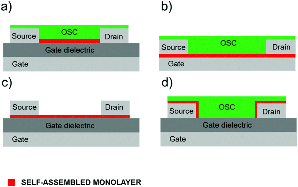 | ||
| Fig. 5 Vertical OFET cross-section. Different SAM usage: (a) gate dielectric primer, (b) molecular dielectric, (c) organic semiconductor and (d) electrode modifier. | ||
3. SAM as a functional coating of gate dielectrics
As discussed above, the interface between the gate dielectric and the OSC thin film is important for charge carrier transport in OFETs (Fig. 6).20,24,109 Charge carriers can be annihilated or trapped at this interface depending on the chemical nature of the dielectric surface, the presence of defects and chemical groups of the non-stoichiometric dielectric, the formation of structural defects in the organic semiconductor layers, and the presence of adsorbates. The presence of water at the interface is also important because the charge carriers (especially cations) can be hydrated by water molecules thus increasing their effective mass (slowing down carrier mobility) or by assisting the hopping by a favorable reorganization energy (enhancing carrier mobility) by polarization.141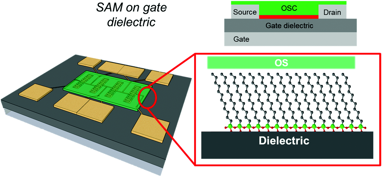 | ||
| Fig. 6 On the left, the schematic cartoon of a silicon-based test-pattern where interdigitated electrodes are coated by an OSC thin-film (green layer). On the right, the magnification of the OSC/gate dielectric interface. | ||
As a prototypical example, we discuss here the silicon oxide surface terminated with silanol groups to show a variety of physico-chemical phenomena and chemical reactions that deplete charge carriers from the channel.
For a p-type organic semiconductor, the charge carrier is localized on a radical cation molecule (OS+). In the presence of water, the following redox reaction leads to the disappearance of the charge carriers (OS):
| 2OS+ + 3H2O ⇄ 2OS + ½O2 + 2H3O+ | (1) |
The presence of silanols yields high surface tension of the dielectric surface favoring water percolation and condensation at the interface.142,145 Being amphoteric, silanol-terminated oxide acts as a base:
| X–Si–OH + H3O+ ⇄ X–Si–(OH2)+ + 2H2O | (2) |
| 2(X–Si–OH) + H3O+ ⇄ (X–Si–O–Si–X) + 2H2O | (3) |
Concerning n-type OSCs, the effect of the underlying substrate has been unambiguously demonstrated by Aguirre et al.,146 who compared Si/SiOx and parylene-based dielectrics. This study allowed them to identify that the hydrated oxygen, namely the chemical couple O2/H2O, is effectively responsible for the suppression of the n-type conduction instead of silanols.147
The following redox reaction
| O2 + 4H+ + 4e− ⇄ 2H2O | (4) |
Owing to these arguments, it is clear that strategies aimed at keeping hydrated oxygen away from the OSC/dielectric interface are crucial for providing stability and reproducibility to OFET operations. The use of SAMs grafted onto the gate dielectrics is thus an effective route to passivate the dielectric surface from undesired reactions and define its surface energy, thus getting rid of several of these problems at once.147,149–154
When a SAM is grafted on a dielectric, the effective capacitance results from the in-series capacitances of the SAM and/or the dielectric. For thick oxide dielectrics, the effective capacitance is dominated by the capacitance of the oxide layer. Grafting a SAM onto hydroxyl-terminated silicon oxide prevents the acid–base and condensation reactions of the silanol groups, as well as it destroys electrostatic interactions, like hydrogen bonds. This hydrophobic surface minimizes electrochemical reactions between the moisture layer at the surface and the charge carriers in the accumulation layer, as previously mentioned.146,148 The existence of such interfacial reactivity was firstly identified for n-type semiconductors on silanol-terminated substrates by Chua et al.,147 and secondly deepened by Aguirre et al.146 This explains the observation of poorer performances of n-type organic semiconductors with respect to p-type ones on test patterns with bare SiOx as the gate dielectric. It clearly points to the fact that the condensation of silanol precursors is functional to avoid the formation of deep trap states.147
Concerning p-type semiconductors, grafting a SAM on silicon oxide is functional to deplete the bias stress originated from the adsorption of hydrated oxygen at the OSC/gate dielectric interface.144 According to Sharma et al.,143,145,155 O2/H2O reacts with holes in the OSC thin-film leading to a dramatic decrease of charge carriers in the conductive channel as in eqn (4). In particular, a negative gate-source bias (VGS) not only produces electrons arising from the water oxidation, but also induces the proton diffusion into the SiOx shifting even more eqn (4) towards the products. This mechanism is consistent with the observation that the transfer characteristics are conserved. This feature, together with the observation that charge carrier mobility remains constant, seems to rule out another possible factor, that is the hydration of the holes by water molecules. This effect would make the effective mass of carriers larger, thus causing a decrease of the charge mobility.142
The presence of a hydrophobic SAM hampers and/or prevents water adsorption at the p-type organic semiconductor/gate dielectric interface from occurring: successful examples have been reported concerning the chemical modification of gate dielectrics such as SiO2 with different SAMs (Fig. 7).
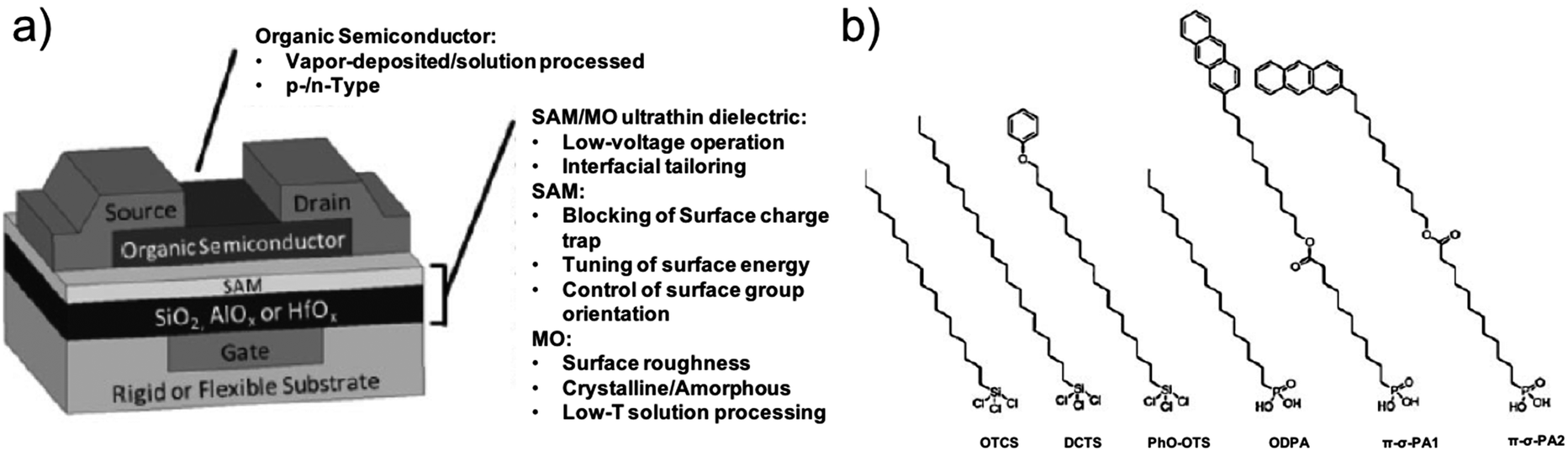 | ||
| Fig. 7 (a) Schematic sketch of a bottom-gate top-contact OFET. (b) Chemical structures of different SAM-forming molecules ref. 109. Copyright © 2010 Wiley-VCH Verlag GmbH & Co. KGaA, Weinheim. | ||
One of the most widely exploited strategies is based on the grafting of alkylsilane SAMs on SiO2, as originally proposed by Jackson's group:156 the performances of a pentacene OFET were dramatically improved by the modification of the silicon oxide surface upon the deposition of a n-octadecyltrichlorosilane (ODTS) monolayer. The change in the performances of such FETs, manifesting itself as a strong decrease of the sub-threshold slope (1.6 V decade−1, while pentacene OFETs with bare SiO2 typically display values of approx. 4–5 V decade−1), was ascribed to the improvement in the molecular organization and the morphology of the organic semiconductor in the first molecular layers closer to the surface. This is an interfacial effect that does not seem to extend deep into the bulk of the pentacene film.
ODTS has been demonstrated as the most effective SAM-forming molecule on silicon oxide dielectrics, because of the compactness of the SAM due to the multiple condensations occurring between adjacent chains. A number of studies addressed the impact of ODTS SAMs on organic thin film devices.109,157–162 Shtein et al.152 observed a drastic reduction of the pentacene grain size of ODTS-modified SiO2 with respect to the untreated dielectric. These morphological improvements were accompanied by a factor three increase of the charge mobility μeff, together with the enhancement of the on/off current ratio. The authors explained their findings by invoking the increased adhesion of the pentacene to the underlying substrate. These results were confirmed by further studies, such as that by Knipp et al.,159 who showed comparable effects of the dielectric surface treatment not only for thermal silicon oxide but also for PECVD silicon nitride. Shankar and Jackson156,162 compared the effects of monolayers of three different compounds, viz. the aforementioned ODTS and its analogues phenyltrichlorosilane (PETS) and t-butyldiphenylchlorosilane, on the morphology of the pentacene layer that was deposited on the SAMs. They found that the morphology of the pentacene was altered by the presence of the alkylsilane SAMs, especially in the first few molecular layers, resulting in improved FET performances.
Once the improvement of the OFET mobility upon modification of the semiconductor/dielectric interface was established, the focus shifted on how the quality of the SAM, depending on its deposition conditions or on the chemical nature of its forming molecules, would play a role. Verlaak et al.163 elucidated the role of SAMs in the modulation of the nucleation free energy of pentacene films under conditions consistent with high-vacuum growth. They highlighted the interplay between the growth rate and surface tension that can change the nucleus critical size and the crystalline polymorph. Depending on the nature of the SAM, the nucleation can be 2D (one-monolayer thick) crystalline nuclei, 3D (more than one monolayer thick), or being completely absent. There are regions in the processing window where 2D and 3D nuclei can coexist, giving rise to the growth of inhomogeneous thin films. This concept was then explored further and demonstrated into a patterning technique by Steudel et al.164 using a wide family of alkylsilane SAMs, including PETS and 10-undecenyltrichlorosilane (UETS). They achieved a systematic change in the nucleation and growth conditions of pentacene film on surfaces where the local surface tension was modulated by the chemical nature of the underlying SAM. Local functionalization of a substrate that enables dimensionally controlled nucleation is an elegant patterning technique for OSC thin films grown by high-vacuum sublimation or deposition.
Lee and co-workers165 deeply investigated the importance of the SAM phase state: they compared the performances of pentacene-based TFTs where the semiconductor layer was deposited on ODTS monolayers displaying different orientations of the aliphatic chains. Better OFET performances were achieved when the pentacene films were grown on more ordered SAMs displaying higher crystallinity (Fig. 8).
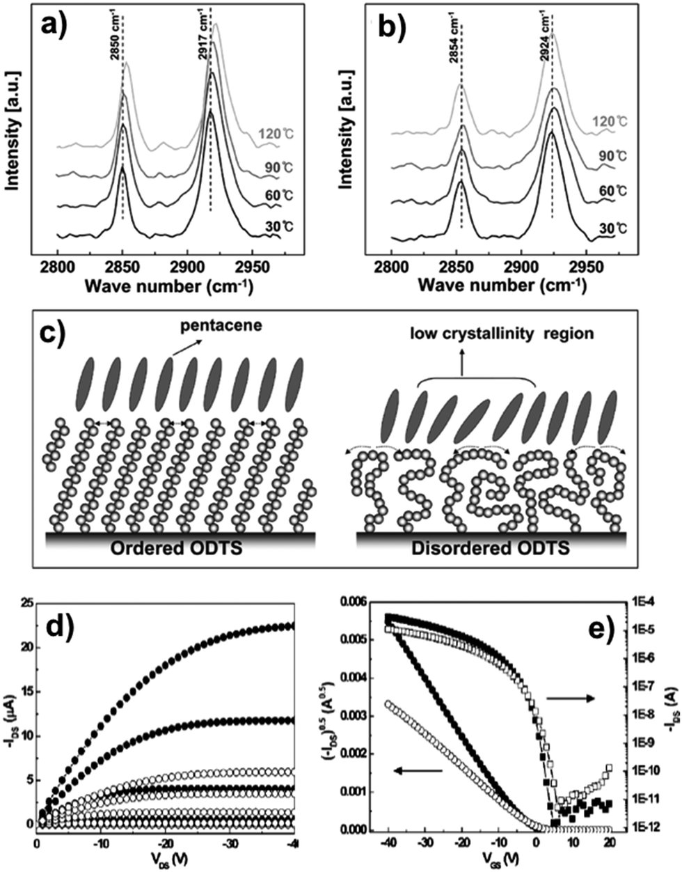 | ||
| Fig. 8 Infrared external reflection spectra of ordered (a) and disordered (b) ODTS monolayers on silicon showing the temperature dependent shifts of asymmetric and symmetric methylene (–CH2–) stretching modes. (c) Cartoon depicting ordered and disordered ODTS monolayers and the pentacene packing onto them. (d) I–V output and (e) transfer characteristics of pentacene TFTs with the gate dielectric treated by ordered (closed symbols) and disordered (open symbols) ODTS monolayers (Tsub 60 °C). Reprinted with permission from ref. 165. Copyright 2008, American Chemical Society. | ||
Dhagat et al.166 investigated how the (in-)homogeneity of ODTS monolayers would cause changes in the properties of 3,4,9,10-perylene-tetracarboxylic bis-benzimidazole (PTCBI) deposited atop the modified insulator, finding that, despite small differences in the unit cell orientation of PTCBI, well ordered SAMs provide enhanced carrier mobility, most likely due to complete passivation of electron trapping silanol groups. Bao and coworkers167 provided evidence for the sensitivity of the nucleation and growth processes of the semiconductor layer to the ODTS layer properties, showing that two-dimensional growth of pentacene was favored by a higher density of the SAM. Later,158 they proposed a novel spin-casting based method to prepare crystalline layers of ODTS on silicon oxide, thus allowing significantly higher charge carrier mobilities for OSCs with respect to amorphous primers. It is important to mention that the compactness and packing of the SAM obtained by condensation of ODTS on the silicon oxide depends on the density of silanol groups at the oxide surface: in native silicon oxide such density is relatively large, but this is not the case in thermal grown silicon oxide. For the effective use of hydrophobic primer SAMs, it is necessary to treat the silicon oxide layer by partial etching of silicon oxide, either by chemical ion etching using piranha solution or ultra-diluted 4% HF solutions, or by reactive ion etching, in order to achieve a sufficiently high density of silanol groups that would allow for the most suitable intermolecular distances for intermolecular cross-linking.
An important contribution to the use of organosilane SAMs between the insulator and the overlaying semiconductor came from Kobayashi et al. (Fig. 9a):150 they showed that by changing the polarity of the SAM-forming molecules it was possible to control the surface carrier density in the organic semiconductor. Comparing TFTs featuring head-groups with markedly different electron affinities, i.e. –CF3 or –NO2 terminated SAMs, the authors observed accumulation of holes or electrons in the conduction channel, and a Vth inversion from +17 to −11 V (Fig. 9b).
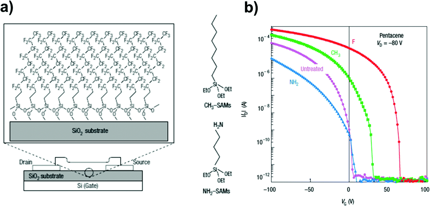 | ||
| Fig. 9 (a) Organic TFTs with perfluorinated SAMs made from (CF3)(CH2)9Si(OC2H5)3 molecules on a SiO2 gate insulator. C60 and pentacene were deposited on the surface of this monolayer. Molecule structures are displayed on the right. (b) Log–Lin plot of IDversus VG for the devices with different SAM treatment. Reprinted with permission from ref. 150. Copyright © 2004, Rights Managed by the Nature Publishing Group. | ||
Their results were further explained by Takeya et al.,151 who could gain deeper insights into the mechanism underlying a Vth shift by investigating single crystal OFETs instead of polycrystalline devices: they demonstrated that hole accumulation in the channel of devices featuring highly electron-affine head-groups occurs at the surface of the OSC single crystal, as a result of charge reorganization at the crystal/oxide interface.
Although ODTS-modified silicon oxide was thoroughly investigated as an example of fine-tuning of electrical performances by chemical modification of the dielectric/semiconductor interfacial region, the ODTS functionalisation is not always straightforward, due to parallel self-polymerisation that yields a polysiloxane thick film covering the substrate.168 In fact, the condensation reaction is autocatalytic as water molecules activate the chlorosilane into reactive silanols. Excess of water, in the absence of controlled relative humidity, leads to the competition of poly-condensation of the precursor molecule instead of surface grafting. Alternative functionalization schemes deprived of the undesired polymerization have therefore been proposed. The most common approach adopted technologically involves the use of organic functionalization of the –OH group on surfaces from silazane precursors. Their reactivity is driven by release of ammonia and avoids parasitic reactions. This scheme is borrowed from the processing steps used in microelectronics. The most widely used precursor is hexamethyldisilazane (HMDS),20,143,144,147,157,169 which causes the hydrophobic functionalization of the silicon oxide surface by forming a silanol bond with the surface. Because of steric hindrance of the tri-methyl-silyl group, this functionalization cannot be strictly classified as a SAM, missing the non-covalent lateral interactions, although sometimes HMDS-grafted films are referred to as SAMs. Along this direction, the work of Yagi et al.169 is relevant, because it highlights that the HMDS-treatment of the SiO2 does improve significantly the electrical performances of OFETs with respect to bare dielectrics, in line with the works employing ODTS monolayers. However, the authors do not ascribe the improvement in the off current to morphological changes, instead to depletion of trap charges at the interface. For these reasons, we do not discuss HMDS-focused work here, and we refer the interested reader to a thorough review by DiBenedetto et al.24
An alternative scheme involves the use of phosponate-terminated organic molecules, which offer the possibility of building SAMs on a variety of dielectrics including high-k materials. Phosphonate SAMs are robust, stable to ambient humidity and exhibit high molecular order.51 Schwartz and co-workers161 introduced phosphonate SAMs, in place of alkylsilanol precursors, on test patterns with silicon oxide gate dielectric. They compared pentacene-based OFETs, one type bearing the standard bare oxide and the other type with 9-phosphonoanthracene SAM as a cushion between the SiO2 gate dielectric and the semiconductor channel. They record an order of magnitude decrease of the sub-threshold slope (from 1–2 V decade−1 to 0.2 V decade−1) and a significant lowering of threshold voltage from 13 V to −4 V. They further investigated the beneficial use of phosphonate-based SAMs in a more comprehensive, comparative study:51 they observed that phosphonate SAMs bearing an alkyl chain yield an OFET response comparable to that of ODTS-functionalized devices. When the phosphonate group is attached to oligothiophene or anthracene moieties to be used as active SAMs (see also Section 6 on SAMFETs), a dramatic improvement in the OFET properties, in terms of sub-threshold slopes of 0.2 V decade−1, reduced trap states, uniform threshold voltage −4.5 V and on/off ratios of 108, is observed.
The use of phosphonic acid SAMs allows one to change both chemistry and morphology of a variety of oxide surfaces, which are technologically interesting because of their high-k dielectric permittivity (Fig. 10).160,170–172 The surfaces of these materials often exhibit a density of defects (as they are non-stoichiometric), substantial roughness, and enhance the polarization effects on charge carriers due to ionic coupling with the oxide lattice.173,174 Kelley et al.175 exploited the high affinity of alkylphosphonic acid for alumina dielectrics to form highly uniform monolayers prior to pentacene deposition, obtaining high field-effect mobility and proposing the use of functionalization steps that, at variance with silane-based chemistry, would not lead to side reactions and unbound reactive groups.
 | ||
| Fig. 10 (a) On top, chemical structures of OSCs and phosphonate SAMs along with the OFET cross section. (b) I–V transfer characteristics and (c) plot of Vth as a function of L. Reprinted with permission from ref. 170. Copyright © 2014 Wiley-VCH Verlag GmbH & Co. KGaA, Weinheim. | ||
Acton et al.160 have systematically investigated variable chain-length alkyl-phosphonic acids on ultra-thin (8 nm thick) hafnium oxide, demonstrating a low voltage–low hysteresis OFET response as a consequence of high-k dielectrics and a planarization with the SAM of an otherwise rough interface. De Leeuw and coworkers reported the use of a phosphonate SAM as a second dielectric on a dual gate transistor based on ZnO as the active layer. The large capacitive coupling, due to the molecular thickness of the SAM dielectric, imparts the device a response to pH that exceeds the Nernst limit, hence enhancing the sensitivity of the transducer.176
The use of SAMs as a dielectric coating has been shown to be effective in other types of nanostructured devices, such as silicon nanowire field effect transistors (Si-NWFETs).177 Although their use has become customary in these devices, we do not treat them here, and direct the reader to dedicated reviews.178,179
To summarize, the common feature of the numerous explored SAMs/OSC combinations is that the deposition of monolayers at the interface between the dielectric and the semiconductor can alter in a very significant manner the performances of the OFET, determining the morphology of the semiconductor layer and its grain size and/or facilitating charge transport by reducing the density of charge trap sites.
It should be said that the most challenging objective, that is to guarantee a high capacitive coupling between the gate and the channel and avoid gate leakage, it is not completely solved in this manner. Although, in principle, SAMs allow one to control the thickness of a dielectric layer with sub-nm accuracy, and to fabricate dielectric layers of a few nm thickness, the effective capacitance of a field effect device is still dominated by the capacitance of the oxide layer for standard dielectric thicknesses (viz. from 100 nm to 300 nm). This hinders the possibility of modulating the gain of the field effect device by means of the SAM. Overcoming this requires the use of ultra-thin dielectric layers that we discuss in detail in Section 4.
4. SAMs as nano dielectrics
In Section 3, we presented examples on the use of SAMs as a coating layer of the gate dielectric, with the aim of modulating the morphology of the OSC layer and/or to decrease the density of charge traps in the channel. Those studies addressed exclusively the modulation of the surface properties of the gate dielectrics at the interface with the organic semiconductor. The adoption of gate dielectric thin films (Fig. 11), featuring both a thickness of tens to hundreds of nanometers and a relative dielectric permittivity of 2–3 (these are standard values for test patterns, also on plastic foils), often imposes large operating voltages, sometimes in excess of 20 V.180 | ||
| Fig. 11 On the left, the schematic cartoon of a silicon-based test-pattern where interdigitated electrodes are coated by an OSC thin-film (green layer). On the right, the magnification of the OSC/gate interface. | ||
Typical capacitance of the metal–insulator–organic semiconductor (MIS) junction is on the order of 10–20 nF cm−2. To increase it, and hence increase the density of charge carriers in the channel, one can either adopt dielectric materials with large permittivity or high-k, or decrease the thickness of the dielectric film. The latter approach cannot be easily solved by simply making the dielectric layer thinner because of defects and undesired current leakage between the channel and the gate.
It turns out that by functionalizing ultra-thin dielectric layers with a highly ordered SAM, the current leakage can be suppressed in a metal–insulator–semiconductor (MIS) junction with silicon as the semiconductor. This concept was demonstrated by Vuillaume and co-workers181 by grafting a 2.8 nm-thick ODTS monolayer on native silicon oxide formed on a p-type doped silicon wafer. The same group investigated ∼2 nm-thick SAMs of long chain, n-alkyltrichlorosilane (CH3–(CH2)n−1–SiCl3, with n = 12, 16, 18) grafted on native oxide on silicon substrates, demonstrating 4–5 orders of magnitude reduction of the leakage current between the semiconductor and the gate electrode with respect to those displayed by bare native silicon oxide and oxynitride of comparable thicknesses.182 The beneficial effect of the SAM was ascribed to the increase of the energy barriers that yields leakage current comparable to standard dielectric (viz. SiOx 200 nm thick).182 The efficiency of the SAM as a dielectric was demonstrated to be directly affected by its packing and order onto the substrate of interest.
The overall capacitance of the MIS structure is the result of the in-series capacitances of the native oxide and the SAM. Owing to the comparable thicknesses (i.e. 1.9 nm for SAM and 1 nm for native oxide) and dielectric constants (i.e. 2.5 for SAM and 3.9 for native oxide), the capacitance would be equivalent to that of a leakage-free native oxide layer whose thickness is about 3 nm. This simple explanation can be thought as a layman rationale to the use of SAMs with ultra-thin inorganic dielectrics: the SAM imparts the insulating layer an almost “ideal” dc dielectric response.
The assessment of the high capacitance achieved by the use of SAMs on native silicon oxide has led to more seminal work by the same group, this time using field-effect transistors.183,184 They exploited alkyltrichlorosilane SAMs, formed on a 1 nm thin native oxide SiO2 layer, as gate dielectrics, in a 25 nm-long gate on a silicon FET.183 Independent of the choice of the terminal group (viz. –CH3, –CH![[double bond, length as m-dash]](https://www.rsc.org/images/entities/char_e001.gif) CH2 and –COOH), low leakage current densities were achieved, ranging from 10−8 to 10−5 A cm−2. They applied a similar derivatization procedure to build a 2 nm thick alkyl chain SAM as a gate insulating film, this time in a α-sexithiophene (α-6T)-based FET.184 The test pattern was fabricated using electron beam lithography on polymethylmethacrylate (PMMA) resist and lift-off. Due to the wettability requirement of PMMA, the choice of the terminal group of the SAM-forming molecules was restricted to the carboxyl-terminated molecules. The OFETs were operated at VGS as low as 2 V, with a field-effect mobility of 3.6 × 10⁻⁴ cm2 V−1 s−1, and despite the molecular thin SAM, they could measure relatively low gate leakage current (approx. 10−6 A cm−2). These were the first examples of the strategy, used in both inorganic183 and organic thin-film transistors (OTFTs),184 of the SAM being used as a dielectric, and not just being deposited on top of it, as it was described in the previous section.
CH2 and –COOH), low leakage current densities were achieved, ranging from 10−8 to 10−5 A cm−2. They applied a similar derivatization procedure to build a 2 nm thick alkyl chain SAM as a gate insulating film, this time in a α-sexithiophene (α-6T)-based FET.184 The test pattern was fabricated using electron beam lithography on polymethylmethacrylate (PMMA) resist and lift-off. Due to the wettability requirement of PMMA, the choice of the terminal group of the SAM-forming molecules was restricted to the carboxyl-terminated molecules. The OFETs were operated at VGS as low as 2 V, with a field-effect mobility of 3.6 × 10⁻⁴ cm2 V−1 s−1, and despite the molecular thin SAM, they could measure relatively low gate leakage current (approx. 10−6 A cm−2). These were the first examples of the strategy, used in both inorganic183 and organic thin-film transistors (OTFTs),184 of the SAM being used as a dielectric, and not just being deposited on top of it, as it was described in the previous section.
This approach was further elaborated by Halik and co-workers:185 they characterized oligothiophene-based OFETs, with the semiconductor being deposited on a 2.5 nm thin ODTS gate dielectric, to systematically investigate the effect of the semiconductor molecular structure, tuned by changing the number of thiophene units and the presence of alkyl side chains as substituents at α and ω positions. They found that the length of the π-conjugated core did not affect the device performances, while the length of the substituted alkyl chain plays an important role, with decyl-substituted sexithiophene showing the best results.
A few years later, Halik et al.186 further improved the performances of their SAM-functionalized devices. To avoid the penetration of the semiconductor molecules within the underlying SAM, they used 18-(phenoxyoctadecyl)trichloro-silane (PhO-ODTS) in place of ODTS, in order to make an extremely dense and compact SAM by exploiting the π–π interaction of the terminal phenyl groups. Their attempt was successful, as their pentacene-based FETs could be operated at low voltages (≤2 V), with leakage current densities as low as 10−9 A cm−2.
Several SAM/OSC combinations were tested in the following years. Park et al.180 grafted a 2.6 nm thick densely packed SAM of docosyltrichlorosilanes (DCTSs) in combination with a polymeric organic semiconductor, namely P3HT, with significant reduction of both the operating voltage and the power dissipation. Besides these promising performances, the advantage of their strategy laid in the choice of uncomplicated functionalization steps, which would not require either specific synthesis of the SAM-forming molecule or vacuum deposition of the semiconductor.
Like in the case of SAMs used as a primer between the gate dielectric and the semiconductor (described in Section 3), phosphonic-based monolayers have been investigated like a viable alternative to organosilanes to be used as nano-dielectrics.187–191 Fukuda et al.190 performed a systematic investigation of pentacene OFETs, whose gate dielectric was composed of SAMs formed by alkyl-phosphonic acids of variable length (CH3(CH2)n−1PO(OH)2, n = 6, 10, 14, 16, and 18) grafted on a 5 nm thick aluminum oxide layer. They could measure a relevant effect of the alkyl chain length on the device properties. As a general rule, SAMs formed by longer alkyl chain molecules would display lower leakage currents than the n-hexyl (n = 6) phosphonic acid SAM, most likely because of a higher extent of intermolecular interactions reducing the liquid-like behaviour and lack of long-range order of monolayers formed by short length species. Very interestingly, they would not observe a monotonic increase of the mobility with the alkyl chain length, as the n-tetradecylphosphonic acid SAM-gate yielding the best values (0.7 cm2 V−1 s−1). By assessing the morphology of the pentacene thin film by AFM, they could relate the superior performances of the n-tetradecylphosphonic acid layer to a significantly lower roughness and larger grain size of the semiconductor, which could be ascribed to a smoother underlying SAM.
A breakthrough in the design of low-operating voltage/high mobility devices came from Klauk et al.187 Aiming at the actual large-scale implementation of SAM-dielectrics in high performance integrated circuits, they opted for an aluminium gate, since this material features both large electrical conductivity and low deposition temperature. They deposited a n-octadecylphosphonic acid (ODPA) SAM on the aluminium native oxide, whose thickness was increased to 3.8 nm by plasma treatment. The densely packed SAM (2.1 nm thick) could reduce the leakage current by three orders of magnitude with respect to the bare oxide, and acted as a better insulator than ODTS, due to a better packing density as revealed by XPS measurements. Importantly, they could prepare low power consumption organic circuits with two different OSCs, such as pentacene and hexadecafluorocopperphthalocyanine (F16CuPc).
Ultra-thin gate dielectrics based on an alkyl-phosphonic acid monolayer grafted on a 4 nm non-stoichiometric aluminium oxide were also employed by Someya's group.191,192 These flexible organic transistors showed superior performances: they demonstrated both a pentacene based, floating-gate non-volatile organic transistor with very small program and erase voltages (−6 to +3 V).192 These devices were 106 nm thick and capable of withstanding extreme bending up to 100 μm radius (Fig. 12).191
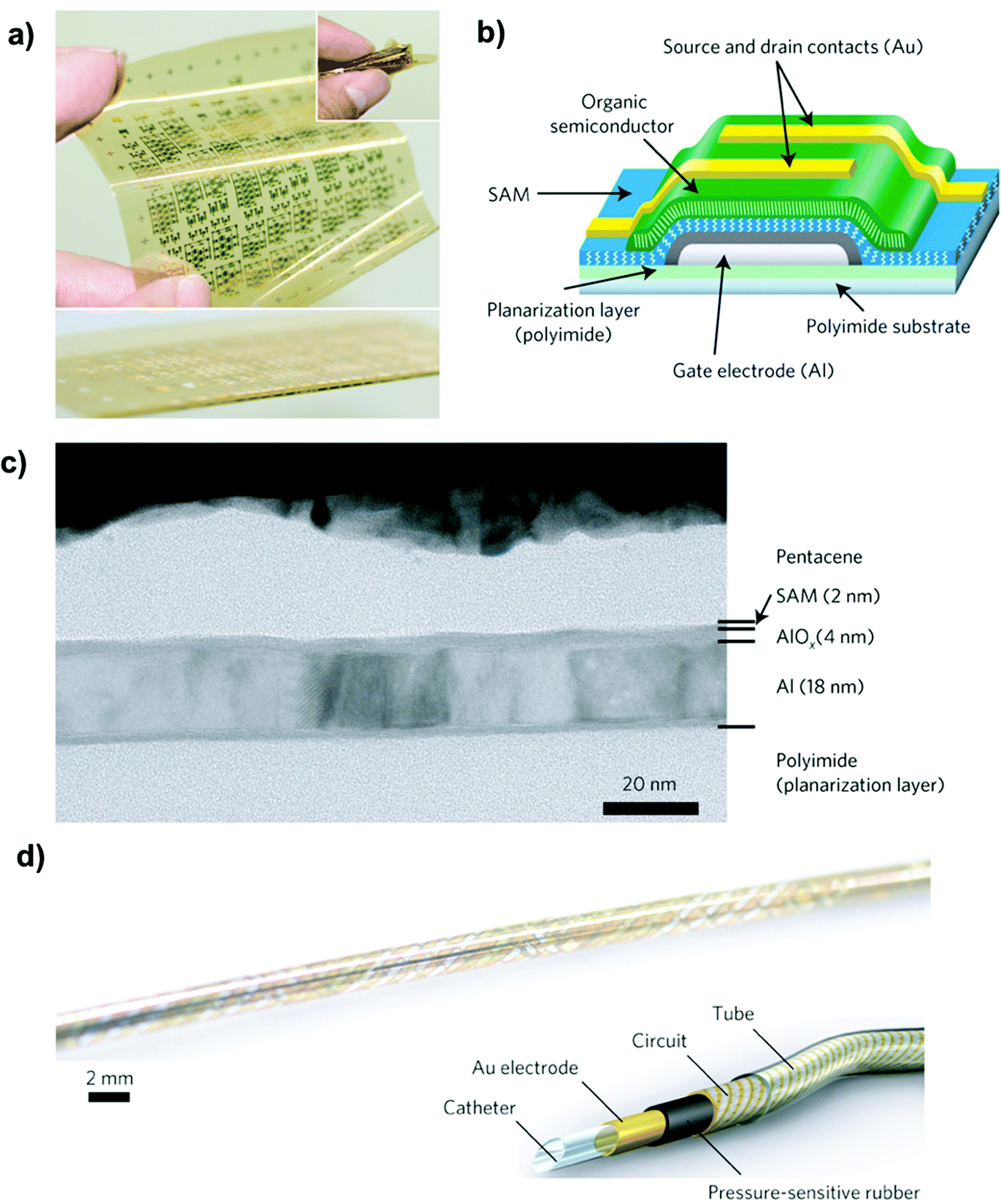 | ||
| Fig. 12 (a) Photograph of a TFT array (total area equal to 75 × 75 mm2). (b) Schematic cross-section of the TFTs. (c) High-resolution cross-sectional electron microscopy image of a flexible TFT. (d) Photograph of a thin catheter that measures the spatial distribution of pressure along its length and circumference by means of an active-matrix sensor helix. Reprinted with permission from ref. 191. Copyright © 2010, Rights Managed by the Nature Publishing Group. | ||
Novak et al.193 proved that the use of gate dielectrics made of phosphonic acid SAMs with markedly different surface energies can be used to modulate the molecular orientation of the first monolayers of α,ω-dihexylquaterthiophene (DH4T), which is reflected in the performances of the OFETs. In particular, they showed that hydrophobic, low surface energy dielectrics favoured edge-on growth of the first two DH4T monolayers, which yields higher charge carrier mobilities.
Although the use of SAM dielectrics can undeniably lead to a marked improvement in the electrical properties of OFETs, the vast majority of the tested SAMs, both based on alkylsilanes and alkylphosphonic acid, exhibits terminal methyl groups, which lower the total surface energy. This limits the choice of formulations of organic semiconductors that can be spin coated on the SAM-based dielectrics. Wöbkenberg et al.194 described an elegant approach to screen the wettability of organic semiconductors by spin coating on OFETs with an Al gate electrode and a gate dielectric made of plasma-generated AlOx and ODPA SAMs. They compared a series of side chain fluorinated methanofullerene or fulleropyrrolidine organic semiconductors based on the spreading parameter ΔW, that is the difference between the work of adhesion and the work of cohesion.195 ΔW serves as a measure of the wettability (tendency of a liquid drop to bind to the solid substrate), to identify the molecules with maximum affinity for methyl-terminated SAMs. Based on this choice, they demonstrated n-channel OFETs with operating voltages of approx. 2 V and mobilities ranging from 0.01 and 0.04 cm2 V−1 s−1.
The perspectives in the field of SAM-based gate dielectrics concern the possibility of exploiting the versatility of the self-assembly approach to explore monolayers endowed with multiple functionalities. Within this respect, Salinas and Halik196 recently demonstrated a DH6T OFET where they incorporated fullerene photoactive derivatives into a tetradecyl phosphonic acid SAM, endowing the device with photo-switchability properties.
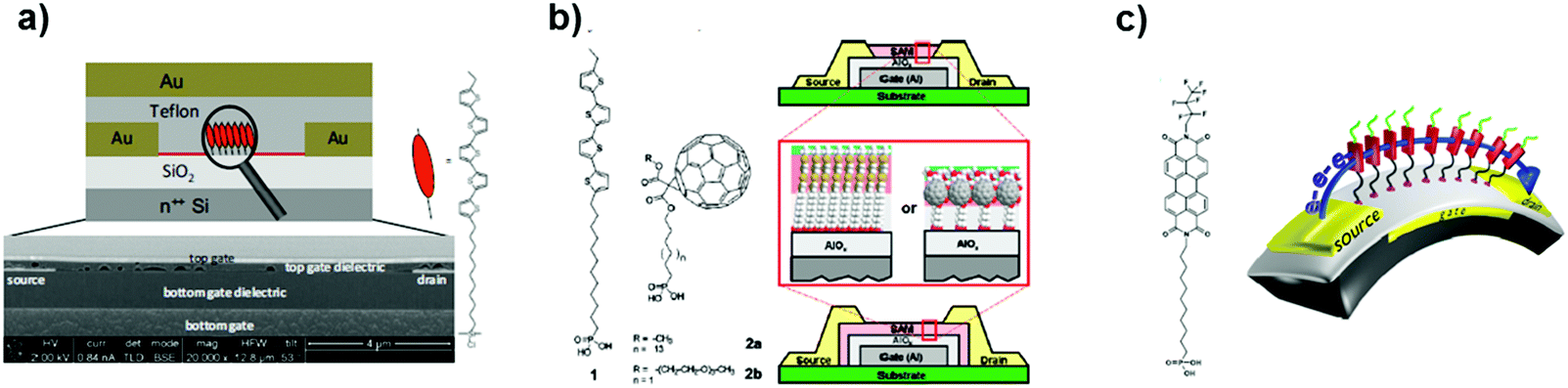
So far, we have described gate nano-dielectrics composed of a single SAM deposited on the device substrate. A somehow different approach to the design of nano-dielectrics was developed by T. Marks' group in 2005, when they pioneered the layer-by-layer self-assembly of σ–π organosilane precursors to build three-dimensional, robust, hybrid organic–inorganic multilayers.197 They built self-assembly multilayers in a modular way, testing different combinations of α-ω-difunctionalized hydrocarbon chains (Alk module), highly polarizable “push–pull” stilbazolium layers (Stb), and a capping layer of octachlorotrisiloxane (Cap) to ensure structural robustness (Fig. 13). The dielectrics prepared with this approach displayed remarkable performances in terms of low leakage, high capacitance and high dielectric constant.
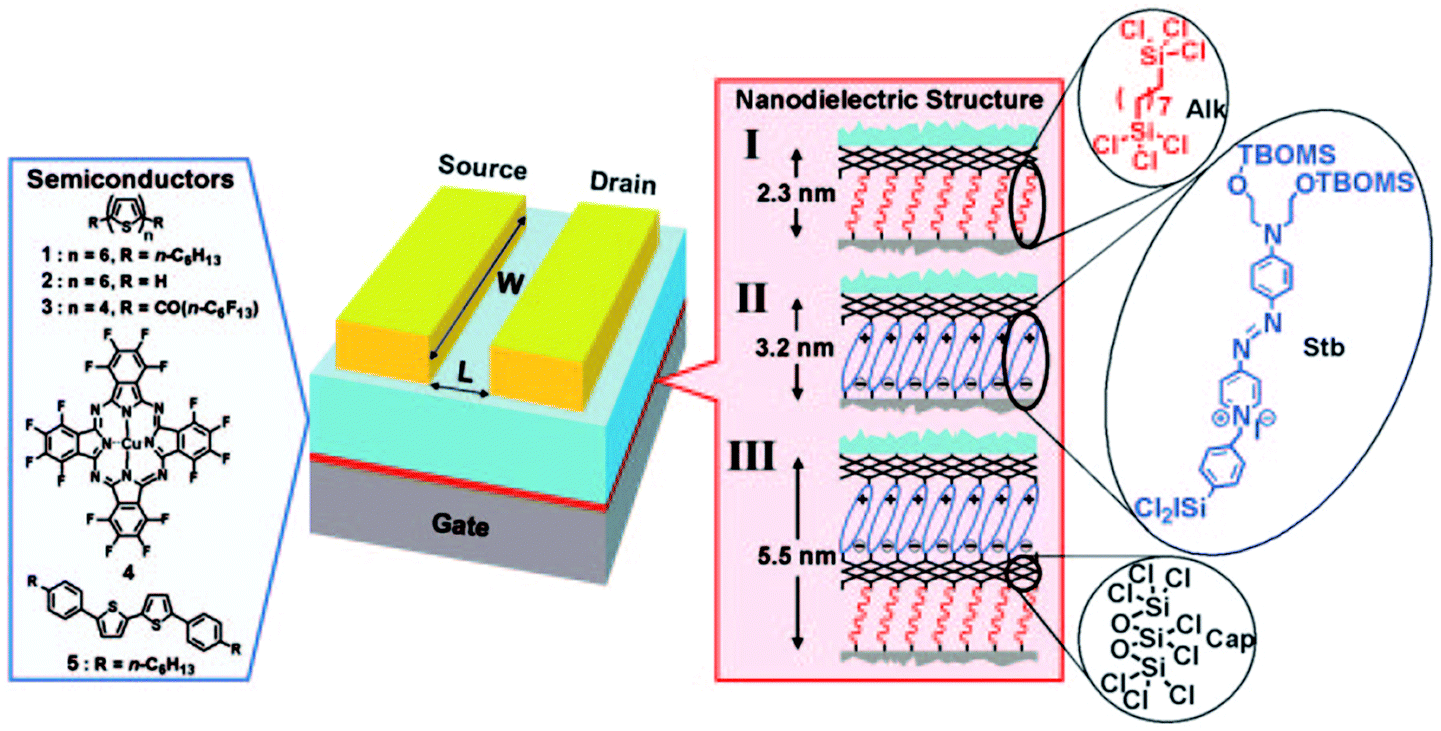 | ||
| Fig. 13 On the left, chemical structures of the OSCs used. On the right, the details of the SAND formation. Reprinted with permission from ref. 197. Copyright © 2005, The National Academy of Sciences. | ||
This seminal paper led to the development of a brand-new field investigating this novel approach to the production of nano-dielectrics, which is now labelled as Self Assembled Nano Dielectrics, SANDs.198–205 Excellent reviews by the Northwestern University group provide further details on the high potential and rapid development of SANDs.206,207
Although numerous examples of SANDs were based on the solution phase self-assembly of multilayers of σ–π organosilane precursors, DiBenedetto et al.198 demonstrated the first nanoscopic gate dielectrics obtained via vapour-phase paving the way for the development of the so-called “v-SANDs”. The π-conjugated building blocks were again based on the Stb group, yielding a 3.6 nm thin organic layer, and a capping layer of SiO2 of approx. 5.9 nm was grown atop to avoid high leakage currents. To exploit the remarkably good insulating properties of their v-SAND, they applied their “dry” bottom up approach to prepare pentacene OTFTs with mobilities of approx. 2 cm2 V−1 s−1, remarkably stable even after a few months.
5. SAM-based semiconductors
In vertical junctions, the charge transport occurs by an intramolecular process, either hopping or through-bond tunneling.208 It is also possible to exploit intermolecular charge transport across the SAM by adopting a planar device configuration. In this case, the fabrication of three terminal devices, like a field effect transistor, where the SAM acts as the conductive channel between source and drain electrodes, can be achieved by means of a self-assembling OSC molecule on the gate dielectric (Fig. 14).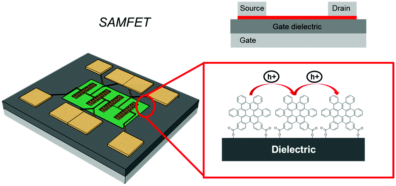 | ||
| Fig. 14 On the left, schematic cartoon of a silicon-based test-pattern where interdigitated electrodes are coated by an OSC thin-film (green layer). On the right, the magnification of the gate dielectric surface is shown where SAM is grafted. | ||
Among the molecules that have been employed to form SAMs acting as OSCs there are oligoacene, oligothienyl, oligophenyl, and perilene derivatives. These devices are termed SAM-based Field-Effect Transistors (SAMFETs).209 In SAMFETs, the thickness and homogeneity of the charge transport layer are strictly controlled through the self-assembly process on the gate dielectric surface, and in principle charge transport layers with no- or minimum domain boundaries could be achieved. SAMFETs are planar Metal–monolayer–Metal (MmM)210,211 junctions endowed with a third electrode (gate) enabling the modulation of charge carrier density. The response to the gate field also allows one to identify the nature of the charge carriers moving through the SAM. Comparing SAMFETs with a standard organic thin-film transistor (OTFT), the major difference consists of the control of the OSC thickness. In the case of SAMFETs, the active layer is formed in a solution at quasi-equilibrium with the substrate containing the test pattern. Importantly, the physical size of the SAM coincides with that of the accumulation layer. In an OFET, the active layer is either grown by high- or ultra-high vacuum techniques under non-equilibrium conditions, as in the case of oligomers or small OSC molecules, else deposited by a wet process, like spin casting, vertical deposition, and zone casting, as in the case of large soluble conjugated molecules or polymers. Moreover, the accumulation layer is restricted to a few molecular layers (equivalent to a few nm) in the case of a molecular semiconductor (like oligoacene, oligothienyl, oligophenyl, and perilene derivatives), even though the thin film is much thicker than this (typically tens of nm). This has some important consequences: SAMFETs are the ultimate OFET devices without an extra capacitance between the accumulation layer and the ambient where they are exposed to, thus making capacitive coupling from the environment extremely efficient; the domain boundaries and defects are minimized, and charge carrier polarization effects due to the idle (namely non-transport active) upper layers are absent. In SAMFETs, the conducting channel enables 2D charge transport within its molecular active film, while “standard” OFETs have a 3D charge transport because they exploit thicker OSC films.112,212,213
The early attempts of fabricating SAMFETs were troubled by process reproducibility.214–216 Kagan et al.217 drew the guidelines for succeeding in this purpose: (i) optimization of the OSC synthesis in order to both minimize by-products and maximize yields; (ii) standardization of the surface engineering to achieve highly ordered molecular assembly onto the dielectric surface and (iii) characterization of the device-molecule structure in terms of structural and electrical features.
The first pursuits exploited SAMs of hexabenzocoronene,214 oligothiophenes215 and tetracene,216 properly tailored to be chemically grafted onto a gate dielectric as alumina or silica. These pioneering works showed the possibility of fabricating SAMFETs for a channel length (L) of few hundreds of nanometers. These attempts highlighted the two main technological challenges: (i) the achievement of devices featuring channel lengths in the scale of microns, and (ii) an efficient electrical contact with the metal electrodes (viz. source and drain).
To solve these high-demanding challenges, a new design of the self-assembling OSC209 was devised by relying on these three key features: (i) a α-substituted quinquethiophene as the semiconducting core, (ii) a dimethylchlorosilane as the anchoring group (instead of trichlorosilane) and (iii) an aliphatic spacer between the semiconducting core and the anchoring group. This design guarantees the best compromise in terms of processability, semiconducting features and long-range packing.
Furthermore, the ohmic contact between the electrode and the SAM-OSC was achieved by chemical etching by means of piranha solution that removes the metal electrode adhesive layer (Cr in this case), leading to an improved charge injection. As a result, SAMFETs were successfully demonstrated featuring a charge mobility of 1.5 × 10⁻² cm2 V−1 s−1 with a channel length up to 40 μm. The SAMFETs were then integrated to form an array of unipolar inverters and in a 15-bit code generator. This novel SAMFET was an ideal benchmark for different purposes: (i) fundamental studies of the charge transport,218,219 (ii) the electrical assessment of different layouts220 and (iii) gas-sensing applications.221
SAMFETs showed a counterintuitive dependence of the channel length (L), showing better performance vs. decreasing L that is the opposite trend with respect to the one commonly observed with OFETs. Mathijssen et al. explained this behaviour in terms of the partial coverage by the SAM on the channel surface for large active device area (Fig. 15).218
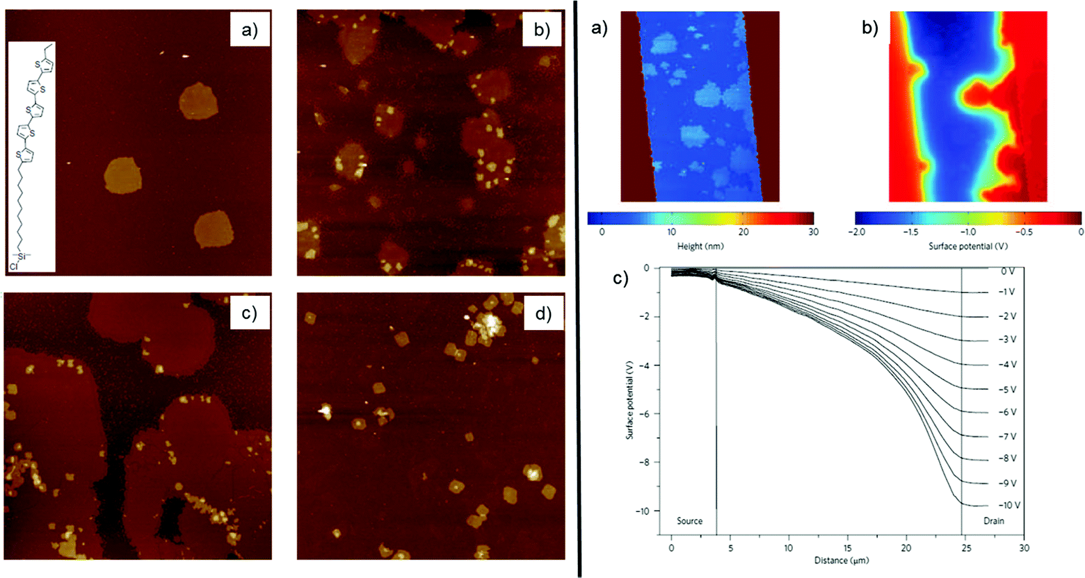 | ||
| Fig. 15 On the left panel, evolution of the SAM coverage in the SAMFET channel by AFM imaging (images area equal to 20 × 20 μm2) for immersion times of 15 min (a), 30 min (b), 1 h (c) and 15 h (d). On the right panel, the AFM image of a partial covered SAMFET (a) and its corresponding potential image (where source and drain are grounded and VGS is −3 V) (b) by using kelvin probe microscopy. (c) Surface potential profile of a fully covered SAMFET featuring VGS = −5 V and VDS swept from O V to −10 V with a pace of −1 V. Reprinted with permission from ref. 218. Copyright © 2009, Rights Managed by the Nature Publishing Group. | ||
Coverage is lower at larger L, whereas at smaller L it becomes close to unity. The big challenge resides in achieving a satisfactory homogeneity compared to vertical junctions fabricated on Au or Ag electrodes. The incomplete SAM exhibits a decrease of the charge mobility (μ) and a positive Vth shift as a function of L. For all these reasons, the device channel must be fully covered by the SAM of interest.218 Soluble OSC (sOSC) molecules capable of strong lateral interactions and flexibility are clearly pursued.
Brondijk et al. investigated charge transport in three FET devices: an (i) oligothienyl-based SAMFET, (ii) an OFET based on molecularly ordered sexithienyl thin films, and (iii) OFETs based on regio-random P3HT.219 These were taken as models for 2D (i and ii) and 3D (iii) charge transport. The I–V characteristics were analysed as a function of temperature. Depending on the dimensionality of transport, the transfer characteristics are expected to obey the following equations219
| I3DDS ∝ (Vth − VGS)2T0/T−1 | (5) |
| I2DDS ∝ (Vth − VGS)T0/T | (6) |
SAMFETs have also been operated in a dual gate architecture featuring good versatility (Fig. 16a).220 Dual gate OFETs have usually two separated conducting channels when the OSC film is thicker than the Debye length, but, in this case, a spatial overlap occurs. In particular, the threshold voltage has been controlled by fixing one gate electrode and varying the other one. As predicted,220 the capacitive coupling governs the Vth shift, whereas contact resistance emerges clearly for the top-gate operation. This stems from the partial electrical shielding of the overhanging source and drain electrodes (due to the under-etching during the fabrication process), which induces a depleted zone at the charge injection interface.
 | ||
| Fig. 16 (a) Schematic picture of the dual gate SAMFET. Reprinted with permission from ref. 220. Copyright © 2010, Rights managed by AIP Publishing LLC. (b) Schematic cross section of thin film transistors p- and n-type. Reprinted with permission from ref. 223. Copyright © 2011, American Chemical Society. (c) Cartoon of a flexible SAMFET. Reprinted with permission from ref. 226. Copyright © 2013 Elsevier B.V. All rights reserved. | ||
The same SAMFET was endowed with a thin layer (10 nm) of porphyrin in order to confer sensitivity towards NO. The high sensitivity (down to ppb content) takes advantage of the molecular thickness of the organic semiconductor. Within this context, it is well documented that lower thicknesses confer higher sensitivity thanks to the direct interaction between the analyte of interest and the conductive channel.222 Other analytes were tested, such as methanol, toluene, and ammonia, but none of them could be sensed. The threshold voltage turned out to be the effective parameter. Likely, the NO–porphyrin adduct yields negative charges, which are responsible for OS doping.221
Another technological breakthrough was the fabrication of low-voltage p- and n-type SAMFETs,223 whose nanometric and hybrid dielectric was composed of AlOx (3.7 nm) plus an alkyl phosphonate chain (around 1.6 nm). This phosphonic tail guarantees a well-packed assembly even though alumina is a rougher substrate than silica. The semiconducting cores were quaterthiophene and fullerene (C60) for hole and electron conduction (Fig. 16b). Concerning n-type SAMFETs, a mixed SAM of C60 functionalized by octadecyl phosphonic acid (C60C18–PA) along with fluorinated dodecyl phosphonic acid (FC12–PA) was shown to improve the overall ordering. The best setup was a ratio of 3![[thin space (1/6-em)]](https://www.rsc.org/images/entities/char_2009.gif) :1 of C60C18–PA and FC12–PA.224 Unfortunately, n-type organic transistors lack stability and reproducibility due to the extreme reactivity of these materials towards moisture and air. Moving from fullerene-based SAMs to perylene derivatives, a step forward was achieved in terms of electron mobility from 10−4 cm2 V−1 s−1 up to 1.5 × 10⁻³ cm2 V−1 s−1. As a result, it was possible to fabricate for the first time complementary inverters fully based on SAMFETs.225
:1 of C60C18–PA and FC12–PA.224 Unfortunately, n-type organic transistors lack stability and reproducibility due to the extreme reactivity of these materials towards moisture and air. Moving from fullerene-based SAMs to perylene derivatives, a step forward was achieved in terms of electron mobility from 10−4 cm2 V−1 s−1 up to 1.5 × 10⁻³ cm2 V−1 s−1. As a result, it was possible to fabricate for the first time complementary inverters fully based on SAMFETs.225
Another advancement related to n-type transistors was their fabrication on flexible substrates (Fig. 16c).226 In particular, PEN foils were used and AlOx was deposited on them before grafting perylene bisimide as an organic semiconductor. This further breakthrough paved the way for disposable devices capable of withstanding mechanical stresses featuring an electron field-effect mobility of 10−3 cm2 V−1 s−1.
Extremely interesting was the exploitation of an α-substituted pentathiophene tailored with 2 C12-alkoxypheny on each side (Fig. 17a). This particular molecule owns the properties of the liquid-crystals, which are able to self-organize once deposited on the gate dielectric by thermal heating (Fig. 17b). The final SAMFET has an improved stability because of the double shielding layer, one placed on top and the other one at the bottom of the semiconducting core.227 Furthermore, the use of HfO2 as a gate dielectric decreases the operational voltages down to few volts. All these properties have been exploited to achieve a SAMFET capable of working in aqueous solution for the first time (Fig. 17c and d).
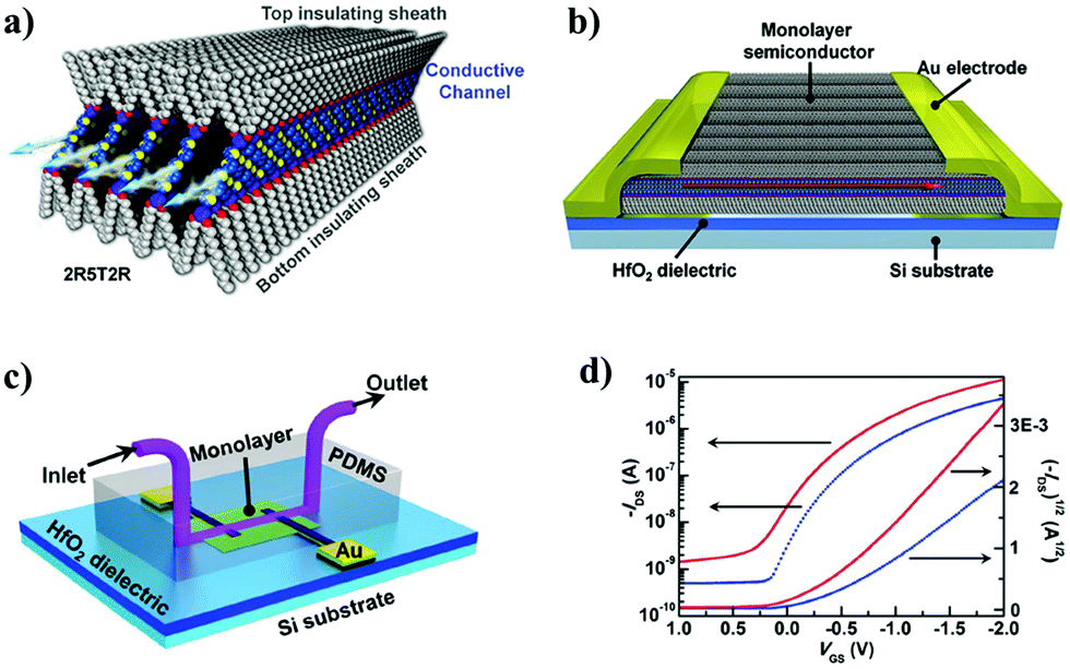 | ||
| Fig. 17 (a) Molecular packing of α-substituted pentathiophene. (b) SAMFET layout. (c) SAMFET operated in aqueous solution by means of microfluidics. (d) I–V transfer characteristics in air (blue line) and in water (red line). Reprinted with permission from ref. 227. Copyright © 2015 Wiley-VCH Verlag GmbH & Co. KGaA, Weinheim. | ||
In conclusion, molecular synthesis of multifunctional self-assembling molecules together with controlled processing has led to a successful development of SAMFETs in the last decade. These transistors offer the possibility of fundamental studies together with the design and prototypization of technological applications. As a result, bending devices, e-nose and integrated circuits (i.e. uni- and bi-polar inverters) have been fabricated showing how molecular electronics can be deployed towards low-cost and disposable devices for point of care tests even in aqueous solution.
6. SAM-functionalised electrodes: bridging molecular and organic electronics
Within the OFET architecture, the remaining role not yet addressed concerns the charge-injection interface, namely the use of the SAMs as metal modifiers (Fig. 18). Here, the attention is focused on the surface engineering of the source (drain) electrode; hence the SAM is part of the planar junction termed metal–insulator–semiconductor (MIS).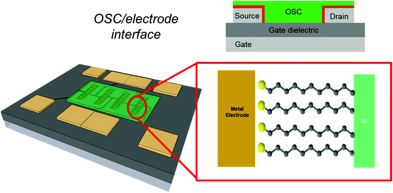 | ||
| Fig. 18 On the left, the schematic cartoon of a silicon-based test-pattern where interdigitated electrodes are coated by an OSC thin-film (green layer). On the right, the magnification of the charge-injection interface. | ||
We discuss here how the concept of SAM-based electronics has evolved through the last few decades from the realm of molecular electronics210,211,228 to that of organic electronics,229 bridging these two fields that were traditionally considered as distinct from the respective communities, despite the fact that similarities in the fundamental properties and unsolved issues exist.
Molecular electronics was envisioned by Aviram and Ratner230 as the control of electron transport across a molecule acting as the active component of a rectifier. The original idea was a molecule with donor and acceptor states at opposite ends bridging two electrodes with a nanometer scale channel (Fig. 19).
 | ||
| Fig. 19 A molecular rectifier envisioned by Aviram and Ratner. Adapted with permission ref. 230. Copyright © 1974 North-Holland Publishing Company. Published by Elsevier B.V. All rights reserved. | ||
Such a concept has been experimentally developed through the years using a variety of experimental solutions: scanning probe microscopes231,232 operated as a local electrode on a vertical junction; planar metal nano-electrodes with a nm channel fabricated by electron beam lithography;233 and mechanically-controlled break junctions.234,235 These solutions achieved single molecular junctions, demonstrating the presence of effects like quantized conductance,236,237 tunneling, hopping, rectification, and in some particular case gain in a three-electrode configuration.238
The consolidation of single molecule experiments into a real technology clashes against problems of reproducibility, robustness, upscaling and integration.239 These were partly intrinsic to the stability of the molecule subjected to a current flowing across it, largely ascribed to the unsolved problem of controlling the structure and configuration of the molecule/electrode interface. Eliminating the contact resistance at the molecule/metal interface was one of the main issues. Owing to the performance variability of the junctions,240 experiments require the acquisition of current–voltage characteristics across datasets including many different molecules/junctions, with a substantial amount of failures.241
Nowadays, molecular electronics is evolving towards devices based on finite ensembles of molecules,241 which is considered a viable route for the miniaturization according to Moore's Law.242 Starting from pioneering evidence on electron tunneling through organic monolayers,243 robust and stable electrical measurements across molecules have been achieved by introducing the vertical molecular junctions where SAMs are sandwiched between two conductive surfaces. In this configuration, there is at least one electrode suited for binding the molecules. The most used substrates are Au or Ag thin films, and therefore the thiol group is the preferred binding moiety. In vertical junctions, charge transport occurs across a large (although finite) number of molecules depending on the contact area of the top electrode. The molecules act as parallel channels for charge transport, as opposed to a single or a few molecules of the local contacts or mechanically-controlled break junctions. The data are renormalized to single molecules upon rescaling of the current density to the area occupied by a molecule on the basal plane, assuming perfect crystal packing in the SAM.241 Either aliphatic chains (as in alkanethiols,121 also terminated with different groups244) or a variety of conjugated molecules (as in oligophenylenes linked to a thiol group) revealed to be suited for charge transport at the molecular length scale.240 These measurements evidenced the exponential decay (i.e. j ≈ j0·exp(−βL)) of the current density as a function of the molecular length L (corresponding to the SAM thickness) and the inverse decay length β, which is associated with the characteristic length-scale of charge tunneling. The quantitative measurements of β tend to display larger values for saturated, aliphatic chains, and smaller values for conjugated moieties with delocalization of π-electrons.30,231,232,240,245
Vertical junctions were achieved with conductive scanning probes, metallic thin films,246 mercury and eutectic alloy drop contacts,17,18,247 nanopores233 as counter-electrodes. Statistical robustness is imparted by the large (albeit finite) number of molecules in the junction, which connect source and drain electrodes. The nature of the head group and the specific interaction with the top electrode play an important role in their electrical characteristics:248 substantial changes in the resistance of the junction are observed, for instance, in the case of mono-thiol versus dithiol-terminated alkanes.241 Within this context, alkane(di-)thiols turned out to be an ideal benchmark to validate molecular junctions and to gain fundamental insights into the charge transport across the SAM.17,231,232,249,250 For instance, Wang et al.233 unambiguously proved through-bond tunneling across alkanethiol by means of nano-pores. To this end, they showed the classical two fingerprints of this mechanism: (i) I–V characteristics independent of temperature (from 80 K to 300 K with a resolution of 10 K) and (ii) exponential decay of current as a function of the chain length (from 8 to 16 methylene units).233
An attempt to upscale the vertical junction into a logic device is a layout based on crossbars sandwiching a SAM. This architecture, termed teramac, comprises an array of independently addressable resistors (or even better a diode to minimize crosstalk) at each node, and is capable of logic operations.251 Both monolayers of rotaxanes that can be electrically switched252–254 and also SAMs were demonstrated,255 opening expectations for real applications. Some controversy about the possible reversible formation of conductive metallic pathways across the gap upon bias prevented the transfer of the crossbars with a SAM into a full-fledged technology.256
Albeit the vertical junction is a transferable platform, reproducible in the laboratory in some of the configurations (e.g. mercury drop), its upscaling to large areas and patterning remains technologically challenging. The deposition process of the top metallic layer from a hot source on top of the SAM causes short-circuits across, making a substantial failure in an ensemble of junctions. A solution to this problem was addressed with the insertion of a conductive polymer, PEDOT:PSS, as a buffer layer for the metallic top electrode. The effective areas are up to 100 μm in diameter with respect to 45 nm of the nano-pores.239 The fabrication of the junctions is completely reproducible (>95%), thus it solves the well-known problems related to shortcuts or other damage of the final molecular junction. This great advancement relies on the use of a PEDOT:PSS layer, which guarantees a perfect electrical connection avoiding the direct deposition of the top metal on the SAM.
Although an OFET has a more complex structure than a vertical junction, it can also be used as a large molecular junction.245 As a result, Stoliar et al. investigated an OFET where a SAM was placed at the source and drain electrodes.121 The planar junction (namely metal/insulator/semiconductor) is formed by Au (e.g. source and drain electrodes), alkanethiol-based SAMs (e.g. insulator) and pentacene thin-films (e.g. OSC). The conductive pentacene channel has a thickness of a few monolayers.111,112 In their work, they investigated a whole series of alkanethiols (from 3 to 16 methylene units). In this way, it was possible to achieve a systematic increase of the thickness of the charge-injection barrier. It turned out that the SAM governs the overall OFET response due to a non-monotonic behavior of the field-effect mobility (μ) as a function of the chain length. In particular, the charge mobility tends to increase at short and intermediate thicknesses (up to 8 methylene units), then to decay exponentially for longer SAMs (>10 methylene units and inverse decay length β = 0.6(±0.1) Å−1). An odd–even effect, viz. fluctuations of the charge mobility values correlated with the parity of the number of carbon atoms in the alkyl chains,257 was observed. The β values were consistent with earlier data obtained with molecular junctions.240,241 Stoliar et al. introduced the concept of “charge-injection length-scale” arising from the complex entanglement of the following factors: (i) morphological disorder of pentacene at the charge-injection interface, (ii) insulating properties of the alkanethiols and (iii) the energetic alignment of the pentacene HOMO and the source/drain work function. The odd–even effect was explained as a result of the anisotropy of the “probe” electrode (viz. pentacene) that is homeotropically standing above the SAM. The odd–even fluctuation then correlates with the orientation of the terminal methyl group with respect to the long axis of pentacene molecules. This work demonstrated that the SAM-functionalized OFET is controlled by charge tunneling and that the device is a sensitive gauge to charge transport across the SAM.29,30,244,245
Whereas two-terminal junctions do not allow one to unambiguously discriminate between electrons and holes as the majority carriers, field-effect transistors allow one to select the type of charge carriers. Along this route, C60 and pentacene OFETs (n- and p-type, respectively) were characterized by using a long SAM, such as 1-hexadecanethiol on source/drain electrodes.258,259 Both cases highlighted a non-ohmic contact due to the distortion of the I–V output characteristics in the linear region. The electrical response was fit by means of the thermionic emission model applied to a double Schottky barrier: the values extracted for β were equal to 1.12(±0.06) Å−1 and 0.91(±0.03) Å−1 for electrons and holes respectively.
The concept of OFET as a charge injection organic gauge (CIOG)29,30 emerged clearly, because it was possible to study the charge transport across different types of SAMs. It was shown how OFETs provide detailed information on the charge injection at the molecular scale, being sensitive to fine differences in the molecular design and surface chemistry.29,30,245,260 The SAMs involved in these studies have a more complex architecture with respect to the usual molecular junctions. Both polar aliphatic SAMs (viz. OH-terminated alkanethiols)244 and π-conjugated ones (viz. oligothiophenes)245 were characterized by a systematic increase of the number of monomer units, and thus of the charge-injection barrier. The multi-parametric response of the OFET allowed the extraction of the decay exponent through different parameters such as mobility, current density and total resistivity (Fig. 20). The extracted β were 0.7(±0.2) Å−1 and 0.24(±0.01) for the SAMs formed by polar aliphatic molecules and oligothiophenes, respectively, in good agreement with the literature.
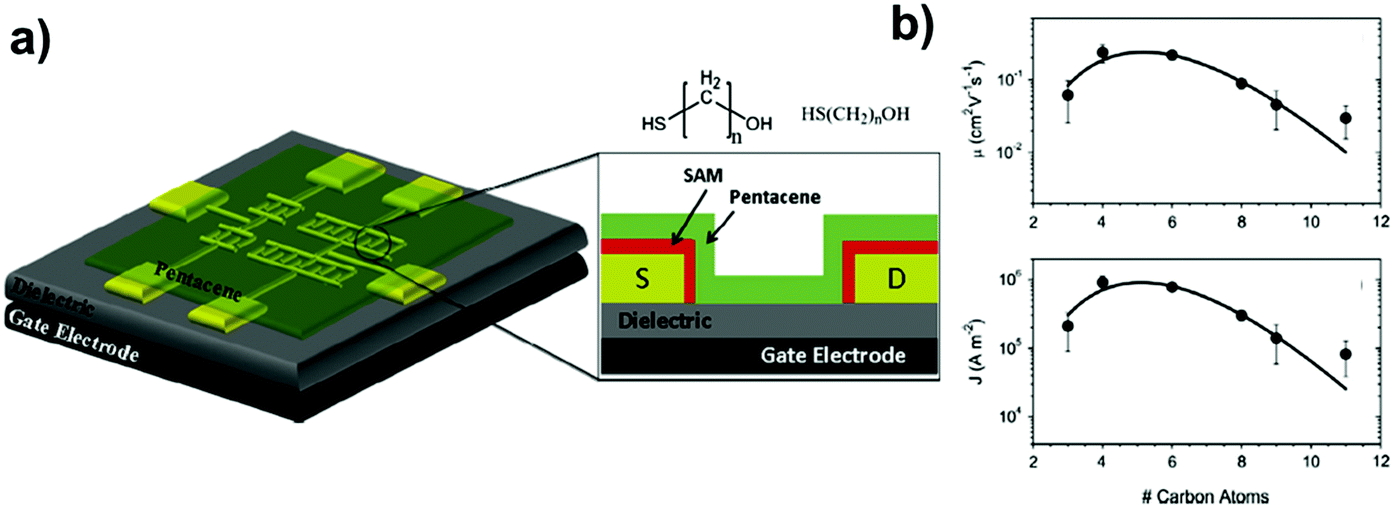 | ||
| Fig. 20 (a) A schematic cartoon of the test pattern shown in ref. 245. The red layer highlights the SAM placed at the charge-injection interface. (b) Log–Lin plot of mobility (μ) and current density (J) vs. number of methylene units in the linear regime (VDS = −1 V). Reprinted with permission ref. 244. Copyright © 2013 Elsevier B.V. All rights reserved. | ||
Asadi et al. provided further insights into the charge transport through SAMs based on hexadecanethiol and perfluorinated decanethiol.261 By comparing contact resistances of functionalized OFETs and the corresponding tunneling resistance extracted by large-area molecular junctions, they proved that the SAM acts as a tunneling resistance in series to the channel one. This work confirmed that it is correct, at a first approximation, to consider the organic semiconductor as the second electrode in a molecular junction layout. This result supported the idea that OFETs with SAMs are ideal test-beds for molecular electronics.121,245
The excellent sensitivity of these devices along with their multi-parametric response makes the OFET a highly informative device for the characterization of the SAM properties, as a function of their molecular structure. For instance, a homologous series of linear mono- and bidentate oligoarylene thiols was successfully used to functionalize OFETs.30 Using SAM-forming units with one or two anchoring groups, or replacing the terminal group (from thiophene to phenyl) induces clear changes in the current density and/or total resistivity. A further example was an OFET functionalized by mono- and bidentate oligoarylene thiols terminated with –OCH3 and –NO2. In this case, the electron-withdrawing feature of the nitro group was successfully detected compared to the methoxy one, because it positively shifts the gate bias at which the field-effect takes place.29 Along this line, it was also possible to monitor the stepwise formation of a multi-layer SAM on source (drain) electrodes. In this case, the OFET successfully sensed the following three functionalization steps: (i) the self-assembly of cysteamine driven by the chemical affinity between the thiol and Au, (ii) the grafting of 4-formilphenylboronic acid through the formation of a Schiff base with cysteamine and (iii) the dopamine esterification once exposed to the surface coated by 4-phenylformylboronic acid.260
The use of SAMs has attracted much attention not only for making charge tunneling devices but also as a bench top viable process for improving the electrical response of OFETs.262,263 As previously stated, SAM functionalization of source/drain electrodes can simultaneously tune a complex combination of phenomena, such as the morphological ordering of the organic semiconductor and the work-function of the metals.121 SAMs are ideal candidates for pursuing this technological objective due to their versatility, sustainability and simplicity (i.e. incubation in an alcohol solution of SAM forming molecules). Since 2000, many examples were proposed.
Hexadecanethiol263 and 4-nitrobenzenethiol264 yielded SAMs capable of greatly improving the OFET performances, whose channel lengths were in the range of 20–70 μm. The former highlighted the beneficial effect of SAMs arising from a more ordered growth of the OSC gaining one order of magnitude in terms of mobility (from 10−2 cm2 V−1 s−1 to 10−1 cm2 V−1 s−1). The latter showed an improved linear region likely due to the electron-withdrawing feature of the –NO2 group. In a coplanar bottom–gate bottom contact architecture, it is rather common to observe dewetting of the OSC at the boundary between gate dielectric and metal electrodes,265 as a result of recrystallization at nuclei formed onto the electrode. The result is that there are discontinuities in the active layer that do not heal during the thin film growth. The use of ultra-thin films, namely one single OSC monolayer, allowed Asadi et al. to correlate the improved performances with the enhanced adhesion properties of OSCs onto the functionalized S/D with respect to the pristine ones.122
The OFET miniaturization, i.e. the shrinking of the channel length from tens of microns to sub-microns, has been a challenge in organic electronics: to solve it, contact resistance has to be minimized.266,267 To this end, SAMs are promising candidates, and especially those formed by highly conjugated molecules, thanks to their better conductivity with respect to aliphatic molecules with larger band gaps. Anthracene-2-thiol268 and thioketone-pentacene269 validated this view, whereas aliphatic molecules were not able to improve the electrical performances with such small L. Furthermore these two SAMs have been tested with pentacene as the OSC, which has a high structural homology for getting an ideal connection. All these data suggested that combining the SAM engineering with a soluble OSC is functional to achieve an effective low-cost fabrication. Gundlach et al. presented the right pair of organic molecules: pentafluorobenzene thiol and the fluorinated 5,11-bis(triethylsilylethynyl) anthradithiophene.270 This combination enabled to yield highly ordered OSC domains up to 10 μm far from the electrode boundary; hence the best performances were obtained for a shorter channel length (i.e. L < 25 μm). This also enabled the low-cost fabrication of flexible circuits with high performances due to the control of the OSC crystallization close to the functionalized electrodes.
Another aspect related to SAMs is the introduction of interfacial dipoles at the interface between the electrode and the organic semiconductor. Many spectroscopic studies proved the SAM capability of tuning the metal work function, which is crucial to avoid an additional charge-injection barrier.271–276 As a consequence, spectroscopic techniques (such as XPS, UPS etc.) were also combined with the electrical characterization of electronic devices,133,277 and it turned out that alkanethiols can tune over a range of 1 eV the Au and Ag work function.278 For this reason, different examples of improvement of electrical performances by SAM functionalization are present in the literature.279–282 Gholamrezaie et al. proved that an energetic barrier between the electrode work function and the OSC HOMO equal to 1.6 eV can be successfully surmounted by using a SAM bearing the proper dipole moment.280 Finally, a wide set of SAMs, ranging from hydrophilic to hydrophobic molecules, were tested with both n- and p-type OSCs.283 The main outcome was a clear correlation between the work function shifts due to SAM functionalization, while mobility did not show any well-defined trend, likely due to additional contribution of the OSC morphology.
The capability of tuning the electrode work function has been extended to the asymmetric functionalization of source and drain electrodes with different SAMs, in order to allow the injection of both holes and electrons. In this manner, it was possible to achieve an ambipolar type of behavior in the OFET also using a traditional p-type OSC as P3HT. In their work, Liscio et al. have shown a method to lift off a SAM from one of the two contact electrodes, and replace it with a second SAM.284 Along this line, adaptive electrode surfaces can be constructed using molecules in the SAM that change configuration from cis-to-trans upon illumination.
In conclusion, the implementation of SAMs on source and drain electrodes in a coplanar architecture can be exploited to simultaneously tune the OSC morphology, the metal work function and the charge carrier transmission across the injection barrier. This configuration allows one to pursue optimization of electrical performances and to perform fundamental studies on the charge carrier transport across SAMs exploiting robust device architecture.
7. New SAM-based device applications
As discussed in the previous sections, SAMs can be deployed either as passive (dielectric) (see Sections 3 and 4) or as active (semiconductor) components (see Sections 5 and 6).20,109,137 In this section, we want to discuss how the dual role of SAMs is exploited in organic electronics to design new SAM-based devices such as synapstors, biosensors, non-volatile memory, and logic circuitry. These examples demonstrate the potential of SAMs as versatile, robust and reliable tools for expanding the purpose of organic electronic devices into multi-sectorial directions: biomedical devices for in vitro experiments, the point-of-care test (POCT), implantable devices, environmental monitoring, wearable electronics, robotics and low cost disposable circuits.A first example is offered by Nanoparticle Organic Memory Field-Effect Transistors (NOMFETs), which are also termed synapstors by merging of two terms: synapse and transistor.285 The synapstor can perform the function of a memory element along with computation. Like a synapse, the NOMFET transforms an AC input signal into an output signal with a precise frequency response and time-modulated amplitude; the modulation can be upward (as in facilitating synapses) or downward (as in depressing synapses). This time response is due to the integration of metallic nanoparticles in the channel of an OFET.286–288 The synapse-like behaviour of these devices arises from the transconductance gain of the transistor along with the capacitance of nanoparticles (NPs) that act as traps with the well energy determined by the NP size/curvature and spatial distribution. On one hand, SAMs grafted onto the device channel are pivotal for the optimum deployment of NPs in the conductive channel and to guarantee a robust adhesion of the active layer; on the other hand, SAMs on the NPs control the inter-NP interactions as well as contribute to their capacitance. The NOMFET layout consists of a bottom-gate coplanar configuration, whose dielectric (SiOx) and source/drain (Au) are functionalized by (3-aminopropyl)trimethoxysilane (APTES) and 2-amino ethanethiol, respectively. In this way, the heterogeneous surface of the device is properly enriched by amine groups, which are responsible for binding Au NPs. Prior to pentacene deposition, the NPs are interconnected by means of alkanedithiols, which act as a tunnelling bridge between them. The memory effect stems from the NPs' capability to store charges, namely holes. Negative gate bias yields positively charged NPs, whereas positive bias discharges them. Comparing NOMFETs and synapses, the holes trapped/released by the NPs act as neurotransmitters, and hence the dynamic control of biological information, termed short-term plasticity (STP), can be successfully mimicked by NOMFETs. This means that high content of holes in NPs induces a depressing biological synapse, if a spike train stimulates NOMFETs. Vice versa, discharged NPs yield a facilitating biological synapse. Furthermore, the STP behaviour has been observed without the initial programming, because the NPs have their discharge time constant, τd (around 20 s). As a result, higher frequencies (T ≪ τd) allow hole trapping into NPs, yielding a depressing trend; in contrast, lower frequencies (T ≫ τd) steer NOMFETs towards facilitating synapses. This kind of device is a promising candidate towards neuromorphic circuitry,289 which is considered as an alternative architecture to the standard von Neumann binary logic and envisioned for ICT applications. At the same time, the NOMFET is suggestive of the possibility of replacing broken synaptic contacts, as in certain pathologies of the central neural system, or due to injuries, thus playing the role of a prosthetic device in neurology and an electroceutic tool for stimulation of nerves and brain.
Regarding OFET sensors, we classify them according to the operating mode or the physical state of the analyte: (i) the dry-state operating mode (termed sometimes e-nose290) to detect gas analytes, and (ii) the wet-state operating mode (termed sometimes e-tongue291,292). A first example of SAM-based gas sensors by Podzorov exploits the alkanetrichlorosilane (both OTS and ODTS) SAM deployed onto either single-crystal OSCs (e.g. rubrene and tetracene)293 or solution-processable polythiophene thin films (viz. P3HT and PBTTT).294 The OSC single-crystals were functionalized with the SAM on their surface, whereas the OSC thin-film is modified within the whole thickness of the film. The driving force for self-assembly is not perfectly understood; however, the comparison of different molecules with the same alkyl residue and different head groups shows that self-assembly occurs only when the silanol group is present. The fluorinated SAMs confer the highest doping effect, thus they increase the OSC conductivity by several orders of magnitude due to their electron-withdrawing effect. Such devices act as chemical sensors towards polar vapours, such as ethanol and acetone. This is due to an increased conformational disorder arising from the penetration of these polar molecules into the SAM. Moisture and apolar vapours cannot be detected, because they are not able to diffuse into the SAM.293
Another example of a gas sensor, as previously described in Section 5, relies on a quinquethiophene SAMFET layout that was endowed with an additional layer of iron porphyrins capable of binding NO.221 This device shows a positive shift of threshold voltage after the NO exposure, likely due to the presence of negative charges arising from NO–porphyrin interaction. The sensitivity was reproducible down to 2.7 ppm within 30 min of analyte exposure.
Two biosensors, operated in the dry state, were successfully proved. The former is based on P3HT, as a semiconducting thin-film, to detect thiolated DNA directly assembled on source/drain electrodes.295 Since DNA is negatively charged, the decrease of current arises from the work-function shift of the metal contacts. This device, which is a single shot non-reversible sensor, can distinguish between the presence of single-stranded DNA and double stranded DNA arising from the hybridization with the complementary sequence, which yields a more packed and denser molecular assembly. The second type of device relied on a dual-gate OFET, whose bottom dielectric was shielded by a HMDS cushion.296 The polystyrene-based top dielectric was tailored by maleimide side-groups, which are crucial for the self-assembly of sulphate binding protein. This biological layer is capable of adsorbing sulphate ions acting as a top gate in the dry operational-mode.
More recently, SAMs have been revisited in the context of label-free organic biosensors operated in aqueous solutions. The SAM main role is to ensure recognition, but, besides imparting the device specificity and selectivity, the monolayer can also impact on the device sensitivity, depending on the molecular design. Electrolyte-gated OFETs (EGOFETs) are among the most investigated layouts for biosensing, drug dispensing297 and transduction of cellular signals.298,299 In these devices a SAM is inserted either at the electrolyte/gate interface or at the OSC/electrolyte interface.300 In both cases the device transduces the change in electrostatic potential, Vg,eff, at the OSC/aqueous solution interface into an electronic signal. The coupling between the device and the aqueous environment is capacitive, and hence sensitivity is higher when the capacitance COSC/aq of the OSC/aqueous interface is the largest.301 In EGOFETs the electrostatic potential Vaq of the solution is fixed by the gate electrode immersed in the solution and is constant throughout the bulk. The potential difference (Vg − VOSC) between the gate voltage and the OSC is partitioned between the gate electrode/aqueous solution interface (Vg − Vaq) and the OSC/aqueous solution interface (Vaq − VOSC) = Vg,eff. Referring to Fig. 3b in the paper by Casalini et al.,302 the voltage drop occurs only at these two interfaces when the electrolyte is a saline solution. A change of the potential drop Δϕ at the gate/aqueous solution interface will change the effective gate potential Vg,eff and hence the signal measured by the OFET according to the formula:
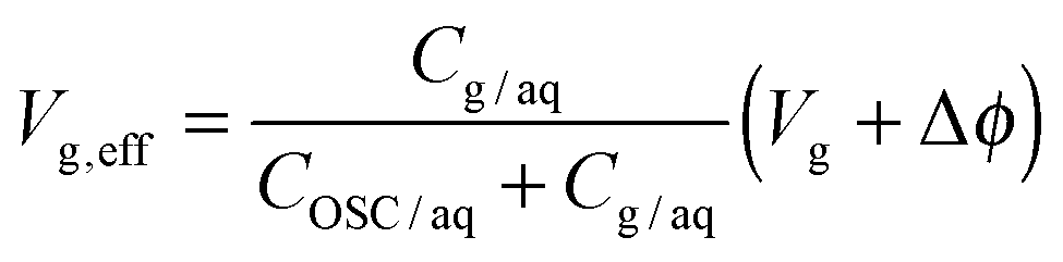 | (7) |
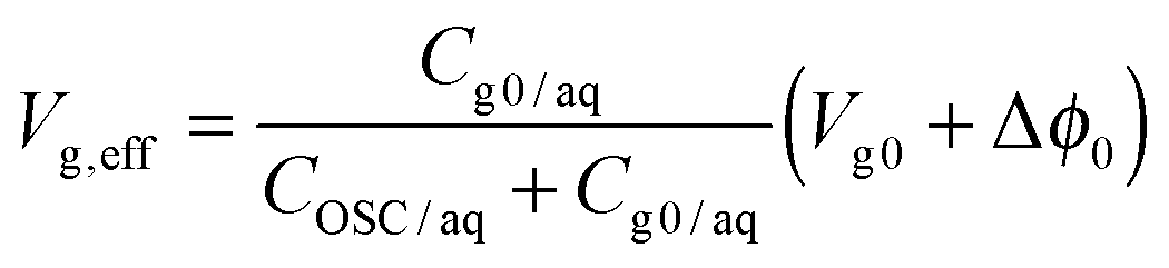 | (8) |
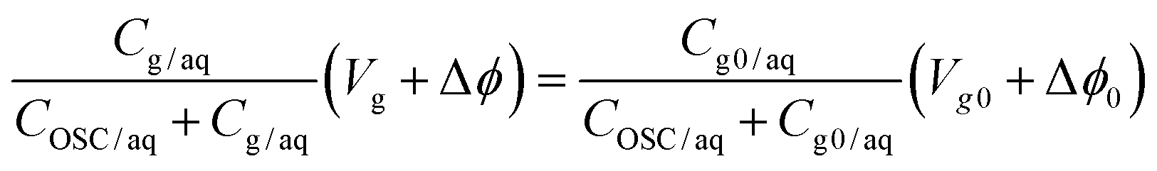 | (9) |
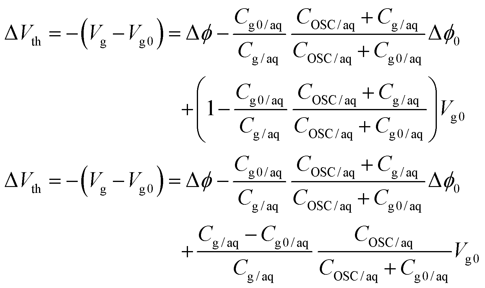 | (10) |
With this architecture, EGOFET sensors have been demonstrated to detect the concentration of a neurotransmitter, dopamine, with sub-nM (10–100 pM) sensitivity (Fig. 21a).303 The dopamine sensor operates by means of a specific recognition element on the gate dielectrics that is assembled through a multi-step SAM composed of (i) cysteamine and (ii) 4-formylphenyl boronic acid on the Au gate.303 The chemical affinity between the boronic moiety and dopamine yielded sensitivity down to pM concentration in reference solutions. Such a concept has been further extended to bio-relevant molecules, like cytokines304 (as pro- and anti-inflammatory biomarkers), or odorant molecules such as (S)-(+) carvone and (R)-(−) carvone (Fig. 21b).305
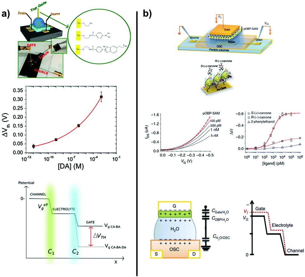 | ||
| Fig. 21 (a) On the left panel, the schematic picture of an EGOFET and the inset shows each SAM steps (1) cysteamine, (2) 4-formylphenyl boronic acid and (3) dopamine. A plot of ΔVth as a function of DA concentration and the rationale of the potential drop between the gate and the OSC. Reprinted with permission from ref. 303. Copyright © 2012 Elsevier B.V. (b) On the right panel, the cartoon of the EGOFET functionalized by the odorant binding molecule. Electrical sensing of the two enantiomers and the equivalent circuit of this device. Reproduced with permission from ref. 305. Copyright © 2015, Rights managed by the Nature Publishing Group. | ||
DNA hybridization has also been successfully detected at the gate surface of OECTs.306 Thiolated DNA was able to yield a molecular layer on the Au gate,306 and its consequent hybridization was detected down to the nM scale. The sensitivity was dramatically increased by using an electrical pulse (down to pM scale) during this biological process. This device senses polar bio-targets, because the recognition event at the gate/electrolyte interface produces interfacial dipoles on the gate surface yielding a threshold voltage shift. The electrostatic coupling at the bio-hybrid interface is not a limiting aspect: as a result, Lin et al.306 show that an increased ionic strength does not affect the sensitivity, ruling out at the zero-th order the capacitive coupling across the Debye Helmholtz layer.
It is also possible to engineer the surface of both organic semiconductors and conductive polymers in order to graft chemically biological probes, such as DNA307 and enzymes (e.g. penicillase308 and glucose oxidase309). The organic semiconductor thin-film is usually hydrophobic, and this hinders a chemical tethering of biological probes (usually water soluble molecules with large polar patches and typically small hydrophobic solvent-exposed regions) without intermediate processing. An EGOFET based on α-sexithiophene (α-6T) has been fabricated as a biosensor towards penicillin. The α-6T was functionalized with a stepwise surface engineering: (i) UV irradiation, (ii) silanization by means of (3-aminopropyl)triethoxysilane (APTES), (iii) amine-to-carboxylic transformation thanks to succinic anhydride and (iv) EDC/NHS activation.308 This protocol leads to the chemical linkage of penicillase, whose catalytic activity hydrolyses the β-lactam ring of penicillin yielding protons as side-products. As a result, the capability of sensing local acidity is the rationale of this bio-sensor. Another example of EGOFET took advantage of a carboxylated P3HT. These pendant groups (namely –COOH) make easier the surface engineering of this OSC, following activation by EDC/NHS click-chemistry.307 In this way, single-stranded DNA was chemically grafted, and its hybridization was sensed down to the nM scale. These approaches highlight how the bio-conjugation techniques lower the hydrophobic barrier of the OSC. Although excellent results are achieved, this phenomenon clearly weakens the capacitive coupling between the electrolyte and the OSC, which is one of the most urgent challenges within this context. Recent advances have been achieved in OECT devices based on PEDOT:PSS. This polymer is not prone to bio-conjugation, since it lacks reactive groups (such as amine, carboxyl and hydroxyl); yet, an addition of poly(vinyl alcohol) to the PEDOT:PSS solution endows the final polymer product with –OH side groups avoiding any worsening of conductance thanks to an appropriate dosing of PVA with respect to the other two components. These hydrophilic groups guide the self-assembly of 3-glycidoxypropyltrimethoxysilane (GOPS) molecules on the conductive polymer surface. This additional layer makes possible the covalent grafting of glucose oxidase, whose catalytic activity is clearly detected by the I–t curve after glucose fuelling.309
As widely explained in Section 4, many OFETs rely on hybrid nano-dielectrics composed of an inorganic oxide coated by a SAM. The most used couple of materials are AlOx and n-alkyl phosphonic acid. This architecture allowed for the fabrication of different technological applications, such as non-volatile memories, sensors of pressure and devices for biomedical applications. These SAM-based devices can be operated at low voltages (namely few volts) and they are highly conformable in terms of flexibility and transparency. Low operational voltages are possible because of the molecular thickness of the dielectric, which increases intrinsically its capacitance. The mechanical compliance takes advantage of the surface chemistry between the substrate and the SAM. The covalent binding guarantees a robust structure and the final SAM acts as a further dielectric between the OSC thin film and the substrate. In this way, the strain effects, arising from the bending and/or stretching of the substrate, are shielded by SAM avoiding fluctuation in the charge-carrier density into the conductive channel.310
Concerning organic non-volatile memories, OFETs were endowed with a control gate and a floating one.311 These are composed of AlOx (4 nm thick) plus an n-alkyl phosphonic acid SAM (2 nm thick). These OFETs had polyethylene naphthalate (PEN), as a polymeric scaffold, and they could work at voltages lower than 2 V. In particular, the OFET layout has the floating gate sandwiched between the regular gate and the organic semiconductor. Program and erase voltages are −6 V and +3 V, respectively. The negative bias leads to charge storage into the floating gate, whereas the positive one discharges it avoiding the damage of the nano-dielectric over 103 cycles (1 cycle means −6 V to +3 V, 1 Hz). A pressure sensor was then fabricated by using a stack of (i) 26 × 26 array of organic memories, (ii) a pressure-sensitive rubber sheet and (iii) another PEN layer with a copper film facing the rubber sheet.311 As a result, applying a program voltage, this sensor is able to store information guided by pressure exerted onto the PEN capping layer. The info storage succeeded for 20 minutes up to 20 hours. Another recent example makes use of the same hybrid nanodielectric for producing an organic device capable of withstanding medical sterilization.312 This is usually performed in different ways: (i) for a few seconds at 150 °C, (ii) 20 minutes at 121 °C and (iii) 30 minutes at 100 °C. No heating processes affect the electrical performances, because DNTT, AlOx/C18-SAM and PI (organic semiconductor, dielectric and scaffold respectively) withstand this range of temperatures. As a result, this OFET is an excellent example of how organic electronics can be implemented in medical apparatus due to its mechanical compliance, heat-resistance and low-power consumption.
The last important examples involve mixed SAMs for fabricating organic non-volatile memories (NVM)313 and logic circuitry,314 such as inverters and ring oscillators. NVMs were composed of Al as the gate electrode covered by its oxide and a mixed SAM of n-octadecyl phosphonic acid (C18) and C60–C18. The fine-tuning of fullerene units in the mixed SAMs confers the capability of storing charges to the OFET. Threshold voltages, hysteresis and on/off ratio are the effective parameters that quantify the memory behaviour. In particular, the best memory feature corresponds to the lowest concentration of C60 units in the mixed SAM (namely 99:1 of C18:C60–C18). Another 2-component SAM has been successfully exploited in OFETs. Alkyl/fluoroalkyl phosphonic acids (18 methylene units) have been assembled in order to fine-tune the threshold voltage of OFETs based on pentacene and hexadecafluoro-copper-phthalocyanine, as p- and n-type OSCs. By increasing the content of fluorine atoms, a positive shift of threshold voltage occurs, in agreement with what is observed for a single-component SAM. This led to the fabrication of different inverters featuring different Vth. The intermediate concentration of alkyl:alkylfluorinated phosphonic acids sets the switching voltage at the centre of the supply voltage range. This allows great noise immunity and even the possibility of building a ring oscillator of 5 complementary inverters working at 1 V.
To summarize, SAM implementation in OFET confers outstanding features, such as low-power consumption and extreme robustness towards mechanical strain, which lead to several technological applications appealing for electronics, biomedicine, and safety.
8. Perspectives and conclusions
In this review, we have summarized the use of SAMs in Organic Electronics with a focus on OFETs. These can be defined as interfacial devices, since their electrical performances are strongly dependent on the nature of OSCs/gate dielectrics and metal contacts/OSC interfaces. For this reason, their performances can be significantly modulated by SAMs. We have shown that SAMs can be used in OFETs either as passive (P) or active (A) components, and more specifically as gate dielectric primers (P), metal modifiers (P), molecular dielectrics (A) and OSCs (A). SAMs serving as gate dielectric primers have been extensively exploited not only for an overall improvement in their lifetime, but also for the control of the switching on (namely Vth tuning). The major advantage of using SAMs as metal modifiers concerns the tuning of the charge injection/withdrawal between the metal contacts and the OSC. On one hand, this specific field of investigation proved how OFETs can be used as large-area molecular junctions (namely charge-injection organic gauge, CIOG) for fundamental studies. On the other hand, this specific usage strongly impacts the stability of the device, as in the previous case of dielectric primers. SAMs as molecular dielectrics replace the standard gate dielectrics, such as SiOx, thus allowing one to achieve thicknesses as low as few nanometers, a fundamental prerequisite to low-power applications. Thanks to a wide range of synthetic routes, SAM-forming molecules can be tailored with different functional groups and arrange into multi-layered gate dielectrics of controlled thickness (viz. self-assembled nano-dielectrics, SANDs). As a consequence, the operational voltages can be drastically reduced down to a few volts. Eventually, SAMs can also be exploited for the direct replacement of the active material (i.e. OSC). De Leeuw et al. demonstrated how the molecular packing and the intermolecular interactions of the SAM-forming molecules are pivotal for the fabrication of SAMFETs. Although their fabrication is rather complex, these devices are extremely interesting for basic studies on the type of charge transport, namely to discern between two-dimensional vs. three-dimensional regime. In most of the SAMFETs, the conductive channel is matching the molecular thickness of the SAM: therefore, direct interaction between the SAM and an analyte of interest leads to significant changes in the conductive channel, making SAMFETs extremely efficient as (bio-)sensing devices.The facile use and intrinsic versatility of SAMs have made them a key ingredient of surface science. We could tentatively describe SAM implementation in organic electronics as divided into three categories, depending on how widespread and solid is their exploitation in the processing of electronic devices. The first one encompasses SAM applications, which are so ubiquitous that have become a routine step in the electronics fabrication, even at an industrial large scale, mostly as gate dielectric primers and electrode modifiers. The second group is composed of examples of SAM-based devices, whose understanding is well-established at the laboratory level, but that, although their potential innovation has been clearly demonstrated, they still require refinements to become part of high-throughput processing strategies. SAMFETs and SANDs are major examples of this category. The last family includes SAM-based devices that are still at the proof-of-concept stage, but that however, thanks to their ground-breaking nature, are boosting the development of edge-cutting technologies in interdisciplinary fields such as organic bioelectronics and/or electroceuticals.
The second and the third categories, with a special attention to the last one, are clearly those with the largest room for improvement, where significant advances are expected in the upcoming years. As many of the hot topics in the scientific panorama, whose fingerprint is interdisciplinarity, we believe that in the upcoming years the SAM usage in organic electronics will aim to further intertwine physics, chemistry and engineering with the biological world.
References
- C. D. Dimitrakopoulos and P. R. L. Malenfant, Adv. Mater., 2002, 14, 99–117 CrossRef CAS.
- G. M. Whitesides and B. Grzybowski, Science, 2002, 295, 2418–2421 CrossRef CAS PubMed.
- S. Zhang, Nat. Biotechnol., 2003, 21, 1171–1178 CrossRef CAS PubMed.
- W. C. Bigelow, E. Glass and W. A. Zisman, J. Colloid Sci., 1947, 2, 563–591 CrossRef CAS PubMed.
- W. C. Bigelow, D. L. Pickett and W. A. Zisman, J. Colloid Sci., 1946, 1, 513–538 CrossRef CAS.
- J. Sagiv, J. Am. Chem. Soc., 1980, 399, 92–98 CrossRef.
- Y. Xia and G. M. Whitesides, Annu. Rev. Mater. Sci., 1998, 28, 153–184 CrossRef CAS.
- F. Schreiber, Prog. Surf. Sci., 2000, 65, 151–257 CrossRef CAS.
- F. Schreiber, J. Phys.: Condens. Matter, 2004, 16, R881–R900 CrossRef CAS.
- J. C. Love, L. A. Estroff, J. K. Kriebel, R. G. Nuzzo and G. M. Whitesides, Chem. Rev., 2005, 105, 1103–1170 CrossRef CAS PubMed.
- C. D. Bain and G. M. Whitesides, J. Am. Chem. Soc., 1989, 111, 7164–7175 CrossRef CAS.
- G. E. Poirier, Chem. Rev., 1997, 97, 1117–1128 CrossRef CAS PubMed.
- A. Badia, R. B. Lennox and L. Reven, Acc. Chem. Res., 2000, 33, 475–481 CrossRef CAS PubMed.
- S. Onclin, B. J. Ravoo and D. N. Reinhoudt, Angew. Chem., Int. Ed., 2005, 44, 6282–6304 CrossRef CAS PubMed.
- A. Ulman, Chem. Rev., 1996, 96, 1533–1554 CrossRef CAS PubMed.
- E. Tran, M. Duati, V. Ferri, K. Müllen, M. Zharnikov, G. M. Whitesides and M. A. Rampi, Adv. Mater., 2006, 18, 1323–1328 CrossRef CAS.
- K. Slowinski, R. V Chamberlain, C. J. Miller and M. Majda, J. Am. Chem. Soc., 1997, 119, 11910–11919 CrossRef CAS.
- R. E. Holmlin, R. Haag, M. L. Chabinyc, R. F. Ismagilov, A. E. Cohen, A. Terfort, M. A. Rampi and G. M. Whitesides, J. Am. Chem. Soc., 2001, 123, 5075–5085 CrossRef CAS PubMed.
- S. Hoeppener, R. Maoz and J. Sagiv, Nano Lett., 2003, 3, 761–767 CrossRef CAS.
- M. Halik and A. Hirsch, Adv. Mater., 2011, 23, 2689–2695 CrossRef CAS PubMed.
- D. L. Allara and R. G. Nuzzo, Langmuir, 1985, 1, 52–66 CrossRef CAS.
- D. L. Allara and R. G. Nuzzo, Langmuir, 1985, 1, 45–52 CrossRef CAS.
- A. Cossaro, R. Mazzarello, R. Rousseau, L. Casalis, A. Verdini, A. Kohlmeyer, L. Floreano, S. Scandolo, A. Morgante, M. L. Klein and G. Scoles, Science, 2008, 321, 943–946 CrossRef CAS PubMed.
- S. A. DiBenedetto, A. Facchetti, M. A. Ratner and T. J. Marks, Adv. Mater., 2009, 21, 1407–1433 CrossRef CAS.
- C. Vericat, M. E. Vela, G. Benitez, P. Carro and R. C. Salvarezza, Chem. Soc. Rev., 2010, 39, 1805–1834 RSC.
- R. Hofer, M. Textor and N. D. Spencer, Langmuir, 2001, 17, 4014–4020 CrossRef CAS.
- T. Y. B. Leung, P. Schwartz, G. Scoles, F. Schreiber and A. Ulman, Surf. Sci., 2000, 458, 34–52 CrossRef CAS.
- W. Azzam, C. Fuxen, A. Birkner, H. T. Rong, M. Buck and C. Woll, Langmuir, 2003, 19, 4958–4968 CrossRef CAS.
- S. Casalini, M. Berto, F. Leonardi, A. Operamolla, C. A. Bortolotti, M. Borsari, W. Sun, R. Di Felice, S. Corni, C. Albonetti, O. Hassan Omar, G. M. Farinola and F. Biscarini, Langmuir, 2013, 29, 13198–13208 CrossRef CAS PubMed.
- S. Casalini, F. Leonardi, C. A. Bortolotti, A. Operamolla, O. H. Omar, L. Paltrinieri, C. Albonetti, G. M. Farinola and F. Biscarini, J. Mater. Chem., 2012, 22, 12155 RSC.
- M. L. Chabinyc, J. C. Love, J. H. Thywissen, F. Cervelli, M. G. Prentiss and G. M. Whitesides, Langmuir, 2003, 19, 2201–2205 CrossRef CAS.
- J. H. Cho, J. A. Lim, J. T. Han, H. W. Jang, J. L. Lee and K. Cho, Appl. Phys. Lett., 2005, 86, 1–3 Search PubMed.
- M. Innocenti, S. Bellassai, C. Bianchini, F. Carlà, F. Loglio, L. Polonia, F. Vizza and M. L. Foresti, Electrochim. Acta, 2010, 55, 2550–2554 CrossRef CAS.
- V. S. Dilimon, J. Denayer, J. Delhalle and Z. Mekhalif, Langmuir, 2012, 28, 6857–6865 CrossRef CAS PubMed.
- P. E. Laibinis, J. J. Hickman, M. S. Wrighton and G. M. Whitesides, Science, 1989, 845 CAS.
- P. E. Laibinis and G. M. Whitesides, J. Am. Chem. Soc., 1992, 114, 9022–9028 CrossRef CAS.
- P. E. Laibinis, G. M. Whitesides, D. L. Allara, Y. T. Tao, A. N. Parikh and R. G. Nuzzo, J. Am. Chem. Soc., 1991, 113, 7152–7167 CrossRef CAS.
- H. Ron, H. Cohen, S. Matlis, M. Rappaport and I. Rubinstein, J. Phys. Chem. B, 1998, 102, 9861–9869 CrossRef CAS.
- C. D. Bain and G. M. Whitesides, J. Am. Chem. Soc., 1989, 111, 7164–7175 CrossRef CAS.
- A. Y. Fadeev, O. A. Soboleva and B. D. Summ, Colloid J. Russ. Acad. Sci., 1997, 59, 222–225 CAS.
- M. Gerunda, C. A. Bortolotti, A. Alessandrini, M. Sola, G. Battistuzzi and P. Facci, Langmuir, 2004, 20, 8812–8816 CrossRef CAS PubMed.
- T. J. Gardner, C. D. Frisbie and M. S. Wrighton, J. Am. Chem. Soc., 1995, 117, 6927–6933 CrossRef CAS.
- E. S. Gawalt, M. J. Avaltroni, N. Koch and J. Schwartz, Langmuir, 2001, 17, 5736–5738 CrossRef CAS.
- M. P. Danahy, M. J. Avaltroni, K. S. Midwood, J. E. Schwarzbauer and J. Schwartz, Langmuir, 2004, 20, 5333–5337 CrossRef CAS PubMed.
- R. Schlapak, D. Armitage, N. Saucedo-zeni, G. Latini, H. J. Gruber, P. Mesquida, Y. Samotskaya, M. Hohage, F. Cacialli and S. Howorka, Langmuir, 2007, 23, 8916–8924 CrossRef CAS PubMed.
- I. M. Tidswell, T. A. Rabedeau, P. S. Pershan, S. D. Kosowsky, J. P. Folkers and G. M. Whitesides, J. Chem. Phys., 1991, 95, 2854 CrossRef CAS.
- E. L. Hanson, J. Schwartz, B. Nickel, N. Koch and M. F. Danisman, J. Am. Chem. Soc., 2003, 125, 16074–16080 CrossRef CAS PubMed.
- E. L. Hanson, J. Guo, N. Koch, J. Schwartz and S. L. Bernasek, J. Am. Chem. Soc., 2005, 127, 10058–10062 CrossRef CAS PubMed.
- J. Schwartz, M. J. Avaltroni, M. P. Danahy, B. M. Silverman, E. L. Hanson, J. E. Schwarzbauer, K. S. Midwood and E. S. Gawalt, Mater. Sci. Eng., C, 2003, 23, 395–400 CrossRef.
- B. M. Silverman, K. A. Wieghaus and J. Schwartz, Langmuir, 2005, 21, 225–228 CrossRef CAS PubMed.
- J. E. McDermott, M. McDowell, I. G. Hill, J. Hwang, A. Kahn, S. L. Bernasek and J. Schwartz, J. Phys. Chem. A, 2007, 111, 12333–12338 CrossRef CAS PubMed.
- G. Gilardi, A. Fantuzzi and S. J. Sadeghi, Curr. Opin. Struct. Biol., 2001, 11, 491–499 CrossRef CAS PubMed.
- D. G. Castner and B. D. Ratner, Biomedical surface science: Foundations to frontiers, Surf. Sci., 2002, 500, 28–60 CrossRef CAS.
- P. Harder, M. Grunze, R. Dahint, G. M. Whitesides and P. E. Laibinis, J. Phys. Chem. B, 1998, 102, 426–436 CrossRef CAS.
- I. Willner and E. Katz, Angew. Chem., Int. Ed., 2000, 39, 1180–1218 CrossRef.
- S. Ferretti, S. Paynter, D. A. Russell, K. E. Sapsford and D. J. Richardson, TrAC, Trends Anal. Chem., 2000, 19, 530–540 CrossRef CAS.
- M. Berggren and A. Richter-Dahlfors, Adv. Mater., 2007, 19, 3201–3213 CrossRef CAS.
- S. K. Arya, P. R. Solanki, M. Datta and B. D. Malhotra, Biosens. Bioelectron., 2009, 24, 2810–2817 CrossRef CAS PubMed.
- C. A. Bortolotti, L. Paltrinieri, S. Monari, A. Ranieri, M. Borsari, G. Battistuzzi and M. Sola, Chem. Sci., 2012, 3, 807 RSC.
- S. Casalini, G. Battistuzzi, M. Borsari, C. A. Bortolotti, G. Di Rocco, A. Ranieri and M. Sola, J. Phys. Chem. B, 2010, 114, 1698–1706 CrossRef CAS PubMed.
- S. Casalini, G. Battistuzzi, M. Borsari, C. A. Bortolotti, A. Ranieri and M. Sola, J. Phys. Chem. B, 2008, 112, 1555–1563 CrossRef CAS PubMed.
- W. Liao, F. Wei, M. X. Qian and X. S. Zhao, Sens. Actuators, B, 2004, 101, 361–367 CrossRef CAS.
- S. Monari, G. Battistuzzi, C. A. Bortolotti, S. Yanagisawa, K. Sato, C. Li, I. Salard, D. Kostrz, M. Borsari, A. Ranieri, C. Dennison and M. Sola, J. Am. Chem. Soc., 2012, 134, 11848–11851 CrossRef CAS PubMed.
- A. Ranieri, G. Battistuzzi, M. Borsari, C. A. Bortolotti, G. Di Rocco and M. Sola, Langmuir, 2012, 28, 15087–15094 CrossRef CAS PubMed.
- D. G. Hoare and D. E. Koshland, J. Biol. Chem., 1967, 242, 2447–2453 CAS.
- E. Ostuni, R. G. Chapman, M. N. Liang, G. Meluleni, G. Pier, D. E. Ingber and G. M. Whitesides, Langmuir, 2001, 17, 6336–6343 CrossRef CAS.
- M. Tirrell, E. Kokkoli and M. Biesalski, Surf. Sci., 2002, 500, 61–83 CrossRef CAS.
- C. R. Emmenegger, E. Brynda, T. Riedel, Z. Sedlakova, M. Houska and A. B. Alles, Langmuir, 2009, 25, 6328–6333 CrossRef CAS PubMed.
- B. A. Holden, M. K. Reddy, P. R. Sankaridurg, B. Rajeev, S. Sharma, M. D. Willcox, C. Morris, D. F. Sweeney and G. N. Rao, Invest. Ophthalmol. Visual Sci., 1997, 38, 981 Search PubMed.
- E. Ostuni, R. G. Chapman, R. E. Holmlin, S. Takayama and G. M. Whitesides, Langmuir, 2001, 17, 5605–5620 CrossRef CAS.
- B. D. Ratner, J. Mol. Recognit., 1996, 9, 617–625 CrossRef CAS PubMed.
- J. Blümmel, N. Perschmann, D. Aydin, J. Drinjakovic, T. Surrey, M. Lopez-Garcia, H. Kessler and J. P. Spatz, Biomaterials, 2007, 28, 4739–4747 CrossRef PubMed.
- L. E. Niklason, J. Gao, W. M. Abbott, K. K. Hirschi, S. Houser, R. Marini and R. Langer, Science, 1999, 284, 489–493 CrossRef CAS PubMed.
- K. Fu, A. M. Klibanov and R. Langer, Nat. Biotechnol., 2000, 18, 24–25 CrossRef CAS PubMed.
- M. U. Kopp, A. J. de Mello and A. Manz, Science, 1998, 280, 1046–1048 CrossRef CAS PubMed.
- K. L. Prime and G. M. Whitesides, J. Am. Chem. Soc., 1993, 115, 10714–10721 CrossRef CAS.
- R. L. C. Wang, H. J. Kreuzer and M. Grunze, J. Phys. Chem. B, 1997, 101, 9767–9773 CrossRef CAS.
- K. Prime and G. Whitesides, Science, 1991, 252, 1164–1167 CrossRef CAS PubMed.
- R. G. Chapman, E. Ostuni, S. Takayama, R. E. Holmlin, L. Yan and G. M. Whitesides, J. Am. Chem. Soc., 2000, 122, 8303–8304 CrossRef CAS.
- R. E. Holmlin, X. Chen, R. G. Chapman, S. Takayama and G. M. Whitesides, Langmuir, 2001, 17, 2841–2850 CrossRef CAS.
- G. Lopez and M. Albers, J. Am. Chem. Soc., 1993, 5877–5878 CrossRef CAS.
- S. Schilp, A. Kueller, A. Rosenhahn, M. Grunze, M. E. Pettitt, M. E. Callow and J. a Callow, Biointerphases, 2007, 2, 143–150 CrossRef CAS PubMed.
- S. Schilp, A. Rosenhahn, M. E. Pettitt, J. Bowen, M. E. Callow, J. A. Callow and M. Grunze, Langmuir, 2009, 25, 10077–10082 CrossRef CAS PubMed.
- S. Balamurugan, L. K. Ista, J. Yan, G. P. López, J. Fick, M. Himmelhaus and M. Grunze, J. Am. Chem. Soc., 2005, 127, 14548–14549 CrossRef CAS PubMed.
- R. J. Jackman, J. L. Wilbur and G. M. Whitesides, Science, 1995, 269, 664–666 CAS.
- M. Mrksich and G. M. Whitesides, Trends Biotechnol., 1995, 13, 228–235 CrossRef CAS.
- J. L. Wilbur, A. Kumar, E. Kim and G. M. Whitesides, Adv. Mater., 1994, 6, 600–604 CrossRef CAS.
- A. Zeira, J. Berson, I. Feldman, R. Maoz and J. Sagiv, Langmuir, 2011, 27, 8562–8575 CrossRef CAS PubMed.
- R. Maoz, E. Frydman, S. R. Cohen and J. Sagiv, Adv. Mater., 2000, 12, 424–429 CrossRef CAS.
- D. S. Ginger, H. Zhang and C. A. Mirkin, Angew. Chem., Int. Ed., 2004, 43, 30–45 CrossRef PubMed.
- L. P. Bauermann, P. Gerstel, J. Bill, S. Walheim, C. Huang, J. Pfeifer and T. Schimmel, Langmuir, 2010, 26, 3774–3778 CrossRef CAS PubMed.
- R. D. Piner, J. Zhu, F. Xu, S. Hong and C. A. Mirkin, Science, 1999, 283, 661–663 CrossRef CAS PubMed.
- S. Hong, J. Zhu and C. A. Mirkin, Science, 1999, 286, 523–525 CrossRef CAS PubMed.
- S. Xu and G. Y. Liu, Langmuir, 1997, 13, 127–129 CrossRef CAS.
- G. Y. Liu, S. Xu and Y. Qian, Acc. Chem. Res., 2000, 33, 457–466 CrossRef CAS PubMed.
- C. E. D. Chidsey, G.-Y. Liu, P. Rowntree and G. Scoles, J. Chem. Phys., 1989, 91, 4421 CrossRef CAS.
- J. Liu, M. J. Casavant, M. Cox, D. A. Walters, P. Boul, W. Lu, A. J. Rimberg, K. A. Smith, D. T. Colbert and R. E. Smalley, Chem. Phys. Lett., 1999, 303, 125–129 CrossRef CAS.
- S. J. Stranick, A. N. Parikh, Y.-T. Tao, D. L. Allara and P. S. Weiss, J. Phys. Chem., 1994, 98, 7636–7646 CrossRef CAS.
- F. Biscarini, Q. K. Ong, C. Albonetti, F. Liscio, M. Longobardi, K. S. Mali, A. Ciesielski, J. Reguera, C. Renner, S. De Feyter, P. Samorì and F. Stellacci, Langmuir, 2013, 29, 13723–13734 CrossRef CAS PubMed.
- A. M. Jackson, J. W. Myerson and F. Stellacci, Nat. Mater., 2004, 3, 330–336 CrossRef CAS PubMed.
- H. X. He, H. Zhang, Q. G. Li, T. Zhu, S. F. Y. Li and Z. F. Liu, Langmuir, 2000, 16, 3846–3851 CrossRef CAS.
- P. Lin and F. Yan, Adv. Mater., 2012, 24, 34–51 CrossRef CAS PubMed.
- J. T. Mabeck and G. G. Malliaras, Anal. Bioanal. Chem., 2006, 384, 343–353 CrossRef CAS PubMed.
- S. Casalini, T. Cramer, F. Leonardi, M. Cavallini and F. Biscarini, Organic Nanomaterials: Synthesis, Characterization and Device Applications, 2013, pp. 397–421 Search PubMed.
- B. G. Horowitz, Adv. Mater., 1998, 10, 365–377 CrossRef.
- J. Zaumseil and H. Sirringhaus, Chem. Rev., 2007, 107, 1296–1323 CrossRef CAS PubMed.
- M. C. J. M. Vissenberg and M. Matters, Phys. Rev. B: Condens. Matter Mater. Phys., 1998, 57, 12964–12967 CrossRef CAS.
- Y. D. Park, J. A. Lim, H. S. Lee and K. Cho, Mater. Today, 2007, 10, 46–54 CrossRef CAS.
- H. Ma, H.-L. Yip, F. Huang and A. K.-Y. Jen, Adv. Funct. Mater., 2010, 20, 1371–1388 CrossRef CAS.
- R. Ruiz, A. Papadimitratos, A. C. Mayer and G. G. Malliaras, Adv. Mater., 2005, 17, 1795–1798 CrossRef CAS.
- A. Shehu, S. D. Quiroga, P. D'Angelo, C. Albonetti, F. Borgatti, M. Murgia, A. Scorzoni, P. Stoliar and F. Biscarini, Phys. Rev. Lett., 2010, 104, 246602 CrossRef PubMed.
- F. Dinelli, M. Murgia, P. Levy, M. Cavallini, F. Biscarini and D. de Leeuw, Phys. Rev. Lett., 2004, 92, 116802 CrossRef PubMed.
- S. G. J. Mathijssen, M.-J. Spijkman, A.-M. Andringa, P. A. van Hal, I. McCulloch, M. Kemerink, R. A. J. Janssen and D. M. de Leeuw, Adv. Mater., 2010, 22, 5105–5109 CrossRef CAS PubMed.
- H. Sirringhaus, Adv. Mater., 2009, 21, 3859–3873 CrossRef CAS.
- J. E. McDermott, M. McDowell, I. G. Hill, J. Hwang, A. Kahn, S. L. Bernasek and J. Schwartz, J. Phys. Chem. A, 2007, 111, 12333–12338 CrossRef CAS PubMed.
- M. Shtein, J. Mapel, J. B. Benziger and S. R. Forrest, Appl. Phys. Lett., 2002, 81, 268–270 CrossRef CAS.
- F. Liscio, C. Albonetti, K. Broch, A. Shehu, S. D. Quiroga, L. Ferlauto, C. Frank, S. Kowarik, R. Nervo, A. Gerlach, S. Milita, F. Schreiber and F. Biscarini, ACS Nano, 2013, 7, 1257–1264 CrossRef CAS PubMed.
- H. S. Lee, D. H. Kim, J. H. Cho, M. Hwang, Y. Jang and K. Cho, J. Am. Chem. Soc., 2008, 130, 10556–10564 CrossRef CAS PubMed.
- S. Y. Yang, K. Shin and C. E. Park, Adv. Funct. Mater., 2005, 15, 1806–1814 CrossRef CAS.
- R. F. De Oliveira, S. Casalini, T. Cramer, F. Leonardi, M. Ferreira, V. Vinciguerra, V. Casuscelli, N. Alves, M. Murgia, L. Occhipinti and F. Biscarini, Flex. Print. Electron., 2016, 1, 1–7 Search PubMed.
- P. Stoliar, R. Kshirsagar, M. Massi, P. Annibale, C. Albonetti, D. M. de Leeuw and F. Biscarini, J. Am. Chem. Soc., 2007, 129, 6477–6484 CrossRef CAS PubMed.
- K. Asadi, Y. Wu, F. Gholamrezaie, P. Rudolf and P. W. M. Blom, Adv. Mater., 2009, 21, 4109–4114 CrossRef CAS.
- C. Bock, D. V. Pham, U. Kunze, D. Käfer, G. Witte and C. Wöll, J. Appl. Phys., 2006, 100, 114517 CrossRef.
- H. E. Katz, J. Johnson, A. J. Lovinger and W. Li, J. Am. Chem. Soc., 2000, 122, 7787–7792 CrossRef CAS.
- I. Kymissis, C. D. Dimitrakopoulos and S. Purushothaman, IEEE Trans. Electron Devices, 2001, 48, 1060–1064 CrossRef CAS.
- Y. Shen, A. R. Hosseini, M. H. Wong and G. G. Malliaras, ChemPhysChem, 2004, 5, 16–25 CrossRef CAS PubMed.
- N. Koch, J. Phys.: Condens. Matter, 2008, 20, 184008 CrossRef.
- J. C. Scott, J. Vac. Sci. Technol., A, 2003, 21, 521 CAS.
- L. Bürgi, T. J. Richards, R. H. Friend and H. Sirringhaus, J. Appl. Phys., 2003, 94, 6129 CrossRef.
- H. Klauk, W. Radlik, W. Weber, L. Zhou, C. D. Sheraw, J. A. Nichols and T. N. Jackson, Solid-State Electron., 2003, 47, 297–301 CrossRef CAS.
- H. Vazquez, Y. J. Dappe, J. Ortega and F. Flores, J. Chem. Phys., 2007, 126, 144703 CrossRef CAS PubMed.
- G. Witte, S. Lukas, P. S. Bagus and C. Wöll, Appl. Phys. Lett., 2005, 87, 1–3 CrossRef.
- I. Campbell, S. Rubin, T. Zawodzinski, J. Kress, R. Martin, D. Smith, N. Barashkov and J. Ferraris, Phys. Rev. B: Condens. Matter Mater. Phys., 1996, 54, 14321–14324 CrossRef.
- B. de Boer, A. Hadipour, M. M. Mandoc, T. van Woudenbergh and P. W. M. Blom, Adv. Mater., 2005, 17, 621–625 CrossRef CAS.
- R. W. Zehner, B. F. Parsons, R. P. Hsung and L. R. Sita, Langmuir, 1999, 15, 1121–1127 CrossRef CAS.
- C. D. Zangmeister, L. B. Picraux, R. D. van Zee, Y. Yao and J. M. Tour, Chem. Phys. Lett., 2007, 442, 390–393 CrossRef CAS.
- S. A. DiBenedetto, A. Facchetti, M. A. Ratner and T. J. Marks, Adv. Mater., 2009, 21, 1407–1433 CrossRef CAS.
- C. Sekine, Y. Tsubata, T. Yamada, M. Kitano and S. Doi, Sci. Technol. Adv. Mater., 2014, 15, 034203 CrossRef.
- N. Crivillers, S. Osella, C. Van Dyck, G. M. Lazzerini, D. Cornil, A. Liscio, F. Di Stasio, S. Mian, O. Fenwick, F. Reinders, M. Neuburger, E. Treossi, M. Mayor, V. Palermo, F. Cacialli, J. Cornil and P. Samorì, Adv. Mater., 2013, 25, 432–436 CrossRef CAS PubMed.
- G. M. Lazzerini, S. Mian, F. Di Stasio, A. Merari Masillamani, N. Crivillers, F. Reinders, M. Mayor, P. Samorì and F. Cacialli, Appl. Phys. Lett., 2012, 101, 203301 CrossRef.
- T. Cramer, T. Steinbrecher, T. Koslowski, D. Case, F. Biscarini and F. Zerbetto, Phys. Rev. B: Condens. Matter Mater. Phys., 2009, 79, 1–10 CrossRef.
- P. A. Bobbert, A. Sharma, S. G. J. Mathijssen, M. Kemerink and D. M. de Leeuw, Adv. Mater., 2012, 24, 1146–1158 CrossRef CAS PubMed.
- A. Sharma, S. G. J. Mathijssen, M. Kemerink, D. M. de Leeuw and P. A. Bobbert, Appl. Phys. Lett., 2009, 95, 253305 CrossRef.
- S. G. J. Mathijssen, M. Kemerink, A. Sharma, M. Cölle, P. A. Bobbert, R. a J. Janssen and D. M. De Leeuw, Adv. Mater., 2008, 20, 975–979 CrossRef CAS.
- A. Sharma, S. G. J. Mathijssen, E. C. P. Smits, M. Kemerink, D. M. De Leeuw and P. A. Bobbert, Phys. Rev. B: Condens. Matter Mater. Phys., 2010, 82, 1–11 Search PubMed.
- C. M. Aguirre, P. L. Levesque, M. Paillet, F. Lapointe, B. C. St-Antoine, P. Desjardins and R. Martel, Adv. Mater., 2009, 21, 3087–3091 CrossRef CAS.
- L.-L. Chua, J. Zaumseil, J.-F. Chang, E. C.-W. Ou, P. K.-H. Ho, H. Sirringhaus and R. H. Friend, Nature, 2005, 434, 194–199 CrossRef CAS PubMed.
- V. Chakrapani, J. C. Angus, A. B. Anderson, S. D. Wolter, B. R. Stoner and G. U. Sumanasekera, Science, 2007, 318, 1424–1430 CrossRef CAS PubMed.
- K. P. Pernstich, S. Haas, D. Oberhoff, C. Goldmann, D. J. Gundlach, B. Batlogg, A. N. Rashid and G. Schitter, J. Appl. Phys., 2004, 96, 6431–6438 CrossRef CAS.
- S. Kobayashi, T. Nishikawa, T. Takenobu, S. Mori, T. Shimoda, T. Mitani, H. Shimotani, N. Yoshimoto, S. Ogawa and Y. Iwasa, Nat. Mater., 2004, 3, 317–322 CrossRef CAS PubMed.
- J. Takeya, T. Nishikawa, T. Takenobu, S. Kobayashi, Y. Iwasa, T. Mitani, C. Goldmann, C. Krellner and B. Batlogg, Appl. Phys. Lett., 2004, 85, 5078–5080 CrossRef CAS.
- M. Shtein, J. Mapel, J. B. Benziger and S. R. Forrest, Appl. Phys. Lett., 2002, 81, 268–270 CrossRef CAS.
- H. S. Lee, D. H. Kim, J. H. Cho, Y. D. Park, J. S. Kim and K. Cho, Adv. Funct. Mater., 2006, 16, 1859–1864 CrossRef CAS.
- H. B. Akkerman, S. C. B. Mannsfeld, A. P. Kaushik, E. Verploegen, L. Burnier, A. P. Zoombelt, J. D. Saathoff, S. Hong, S. Atahan-Evrenk, X. Liu, A. Aspuru-Guzik, M. F. Toney, P. Clancy and Z. Bao, J. Am. Chem. Soc., 2013, 135, 11006–11014 CrossRef CAS PubMed.
- A. Sharma, S. G. J. Mathijssen, T. Cramer, M. Kemerink, D. M. De Leeuw and P. A. Bobbert, Appl. Phys. Lett., 2010, 96, 12–15 Search PubMed.
- T. N. Jackson, Y. Lin, S. Member and D. J. Gundlach, IEEE J. Sel. Top. Quantum Electron., 1998, 4, 100–104 CrossRef CAS.
- Y. D. Park, J. A. Lim, H. S. Lee and K. Cho, Mater. Today, 2007, 10, 46–54 CrossRef CAS.
- Y. Ito, A. A. Virkar, S. Mannsfeld, J. H. Oh, M. Toney, J. Locklin and Z. Bao, J. Am. Chem. Soc., 2009, 131, 9396–9404 CrossRef CAS PubMed.
- D. Knipp, R. A. Street, A. Völkel and J. Ho, J. Appl. Phys., 2003, 93, 347 CrossRef CAS.
- O. Acton, G. G. Ting, P. J. Shamberger, F. S. Ohuchi, H. Ma and A. K. Y. Jen, ACS Appl. Mater. Interfaces, 2010, 2, 511–520 CAS.
- M. McDowell, I. G. Hill, J. E. McDermott, S. L. Bernasek and J. Schwartz, Appl. Phys. Lett., 2006, 88, 23–26 CrossRef.
- K. Shankar and T. N. Jackson, J. Mater. Res., 2004, 19, 2003–2007 CrossRef CAS.
- S. Verlaak, S. Steudel, P. Heremans, D. Janssen and M. Deleuze, Phys. Rev. B: Condens. Matter Mater. Phys., 2003, 68, 195409 CrossRef.
- S. Steudel, D. Janssen, S. Verlaak, J. Genoe and P. Heremans, Appl. Phys. Lett., 2004, 85, 5550–5552 CrossRef CAS.
- H. S. Lee, D. H. Kim, J. H. Cho, M. Hwang, Y. Jang and K. Cho, J. Am. Chem. Soc., 2008, 130, 10556–10564 CrossRef CAS PubMed.
- P. Dhagat, H. M. Haverinen, R. J. Kline, Y. Jung, D. A. Fischer, D. M. DeLongchamp and G. E. Jabbour, Adv. Funct. Mater., 2009, 19, 2365–2372 CrossRef CAS.
- A. Virkar, S. Mannsfeld, J. H. Oh, M. F. Toney, Y. H. Tan, G. Liu, J. C. Scott, R. Miller and Z. Bao, Adv. Funct. Mater., 2009, 19, 1962–1970 CrossRef CAS.
- A. N. Parikh, M. A. Schivley, E. Koo, K. Seshadri, D. Aurentz, K. Mueller and D. L. Allara, J. Am. Chem. Soc., 1997, 119, 3135–3143 CrossRef CAS.
- I. Yagi, K. Tsukagoshi and Y. Aoyagi, Appl. Phys. Lett., 2005, 86, 1–3 CrossRef.
- U. Kraft, M. Sejfic, M. J. Kang, K. Takimiya, T. Zaki, F. Letzkus, J. N. Burghartz, E. Weber and H. Klauk, Adv. Mater., 2015, 27, 207–214 CrossRef CAS PubMed.
- O. Acton, G. G. Ting II, H. Ma, D. Hutchins, Y. Wang, B. Purushothaman, J. E. Anthony and A. K.-Y. Jen, J. Mater. Chem., 2009, 19, 7929 RSC.
- O. Acton, G. Ting, H. Ma, J. W. Ka, H. L. Yip, N. M. Tucker and A. K. Y. Jen, Adv. Mater., 2008, 20, 3697–3701 CrossRef CAS.
- S. E. Fritz, T. W. Kelley and C. D. Frisbie, J. Phys. Chem. B, 2005, 109, 10574–10577 CrossRef CAS PubMed.
- I. N. Hulea, S. Fratini, H. Xie, C. L. Mulder, N. N. Iossad, G. Rastelli, S. Ciuchi and A. F. Morpurgo, Nat. Mater., 2006, 5, 982–986 CrossRef CAS PubMed.
- T. W. Kelley, L. D. Boardman, T. D. Dunbar, D. V Muyres, M. J. Pellerite and T. P. Smith, J. Phys. Chem. B, 2003, 107, 5877–5881 CrossRef CAS.
- M. Spijkman, E. C. P. Smits, J. F. M. Cillessen, F. Biscarini, P. W. M. Blom and D. M. De Leeuw, Appl. Phys. Lett., 2011, 98, 2012–2015 CrossRef.
- Y. Cui, Q. Wei, H. Park and C. M. Lieber, Science, 2001, 293, 1289–1292 CrossRef CAS PubMed.
- W. Lu and C. M. Lieber, J. Phys. D: Appl. Phys., 2006, 39, R387–R406 CrossRef CAS.
- K. I. Chen, B. R. Li and Y. T. Chen, Nano Today, 2011, 6, 131–154 CrossRef CAS.
- Y. D. Park, D. H. Kim, Y. Jang, M. Hwang, J. A. Lim and K. Cho, Appl. Phys. Lett., 2005, 87, 1–3 Search PubMed.
- P. Fontaine, D. Goguenheim, D. Deresmes, D. Vuillaume, M. Garet and F. Rondelez, Appl. Phys. Lett., 1993, 62, 2256–2258 CrossRef CAS.
- C. Boulas, J. Davidovits, F. Rondelez and D. Vuillaume, Phys. Rev. Lett., 1996, 76, 4797–4800 CrossRef CAS PubMed.
- J. Collet and D. Vuillaume, Appl. Phys. Lett., 1998, 73, 2681–2683 CrossRef CAS.
- J. Collet, O. Tharaud, A. Chapoton and D. Vuillaume, Appl. Phys. Lett., 2000, 76, 1941–1943 CrossRef CAS.
- M. Halik, H. Klauk, U. Zschieschang, G. Schmid, S. Ponomarenko, S. Kirchmeyer and W. Weber, Adv. Mater., 2003, 15, 917–922 CrossRef CAS.
- M. Halik, H. Klauk, U. Zschieschang, G. Schmid, C. Dehm, M. Schütz, S. Maisch, F. Effenberger, M. Brunnbauer and F. Stellacci, Nature, 2004, 431, 963–966 CrossRef CAS PubMed.
- H. Klauk, U. Zschieschang, J. Pflaum and M. Halik, Nature, 2007, 445, 745–748 CrossRef CAS PubMed.
- H. Ma, O. Acton, G. Ting, J. W. Ka, H. L. Yip, N. Tucker, R. Schofield and A. K. Y. Jen, Appl. Phys. Lett., 2008, 92, 2006–2009 Search PubMed.
- J. M. Ball, P. H. Wöbkenberg, F. Colĺaux, M. Heeney, J. E. Anthony, I. McCulloch, D. D. C. Bradley and T. D. Anthopoulos, Appl. Phys. Lett., 2009, 95, 93–96 CrossRef.
- K. Fukuda, T. Hamamoto, T. Yokota, T. Sekitani, U. Zschieschang, H. Klauk and T. Someya, Appl. Phys. Lett., 2009, 95, 153306 Search PubMed.
- T. Sekitani, U. Zschieschang, H. Klauk and T. Someya, Nat. Mater., 2010, 9, 1015–1022 CrossRef CAS PubMed.
- T. Sekitani, T. Yokota, U. Zschieschang, H. Klauk, S. Bauer, K. Takeuchi, M. Takamiya, T. Sakurai and T. Someya, Science, 2009, 326, 1516–1519 CrossRef CAS PubMed.
- M. Novak, T. Schmaltz, H. Faber and M. Halik, Appl. Phys. Lett., 2011, 98, 093302 CrossRef.
- P. H. Wöbkenberg, J. Ball, F. B. Kooistra, J. C. Hummelen, D. M. De Leeuw, D. D. C. Bradley and T. D. Anthopoulos, Appl. Phys. Lett., 2008, 93, 013303 CrossRef.
- D. Gentili, G. Foschi, F. Valle, M. Cavallini and F. Biscarini, Chem. Soc. Rev., 2012, 41, 4430 RSC.
- M. Salinas and M. Halik, Appl. Phys. Lett., 2013, 102, 203301 CrossRef.
- M. Yoon, A. Facchetti and T. J. Marks, Proc. Natl. Acad. Sci. U. S. A., 2005, 102, 4678–4682 CrossRef CAS PubMed.
- S. A. DiBenedetto, D. Frattarelli, M. a Ratner, A. Facchetti and T. J. Marks, J. Am. Chem. Soc., 2008, 130, 7528–7529 CrossRef CAS PubMed.
- L. Wang, M. H. Yoon, A. Facchetti and T. J. Marks, Adv. Mater., 2007, 19, 3252–3256 CrossRef CAS.
- S. Ju, K. Lee, M.-H. Yoon, A. Facchetti, T. J. Marks and D. B. Janes, Nanotechnology, 2007, 18, 155201 CrossRef.
- H. C. Lin, P. D. Ye, Y. Xuan, G. Lu, A. Facchetti and T. J. Marks, Appl. Phys. Lett., 2006, 89, 1–4 Search PubMed.
- S. Ju, K. Lee, D. B. Janes, R. C. Dwivedi, H. Baffour-Awuah, R. Wilkins, M. H. Yoon, A. Facchetti and T. J. Mark, Appl. Phys. Lett., 2006, 89, 1–4 Search PubMed.
- S. Ju, D. B. Janes, G. Lu, A. Facchetti and T. J. Marks, Appl. Phys. Lett., 2006, 89, 193506 CrossRef.
- S. H. Hur, M. H. Yoon, A. Gaur, M. Shim, A. Facchetti, T. J. Marks and J. A. Rogers, J. Am. Chem. Soc., 2005, 127, 13808–13809 CrossRef CAS PubMed.
- S. Ju, K. Lee, D. B. Janes, M. H. Yoon, A. Facchetti and T. J. Marks, Nano Lett., 2005, 5, 2281–2286 CrossRef CAS PubMed.
- A. Facchetti, M.-H. Yoon and T. J. Marks, Adv. Mater., 2005, 17, 1705–1725 CrossRef CAS.
- P. Ortiz, A. Facchetti and T. J. Marks, Chem. Rev., 2010, 110, 205–239 CrossRef PubMed.
- S. H. Choi, B. Kim and C. D. Frisbie, Science, 2008, 320, 1482–1486 CrossRef CAS PubMed.
- E. C. P. Smits, S. G. J. Mathijssen, P. A. van Hal, S. Setayesh, T. C. T. Geuns, K. A. H. A. Mutsaers, E. Cantatore, H. J. Wondergem, O. Werzer, R. Resel, M. Kemerink, S. Kirchmeyer, A. M. Muzafarov, S. A. Ponomarenko, B. de Boer, P. W. M. Blom and D. M. de Leeuw, Nature, 2008, 455, 956–959 CrossRef CAS.
- J. R. Heath and M. A. Ratner, Phys. Today, 2003, 43–49 CrossRef CAS.
- D. Vuillaume, C. R. Phys., 2008, 9, 78–94 CrossRef CAS.
- G. Horowitz, J. Mater. Res., 2004, 19, 1946–1962 CrossRef CAS.
- E. L. Granstrom and C. D. Frisbie, J. Phys. Chem. B, 1999, 103, 8842–8849 CrossRef CAS.
- X. Guo, M. Myers, S. Xiao, M. Lefenfeld, R. Steiner, G. S. Tulevski, J. Tang, J. Baumert, F. Leibfarth, J. T. Yardley, M. L. Steigerwald, P. Kim and C. Nuckolls, Proc. Natl. Acad. Sci. U. S. A., 2006, 103, 11452–11456 CrossRef CAS PubMed.
- M. Mottaghi, P. Lang, F. Rodriguez, A. Rumyantseva, A. Yassar, G. Horowitz, S. Lenfant, D. Tondelier and D. Vuillaume, Adv. Funct. Mater., 2007, 17, 597–604 CrossRef CAS.
- G. S. Tulevski, Q. Miao, M. Fukuto, R. Abram, B. Ocko, R. Pindak, M. L. Steigerwald, C. R. Kagan and C. Nuckolls, J. Am. Chem. Soc., 2004, 126, 15048–15050 CrossRef CAS PubMed.
- C. R. Kagan, A. Afzali, R. Martel, L. M. Gignac, P. M. Solomon, A. G. Schrott and B. Ek, Nano Lett., 2003, 3, 119–124 CrossRef CAS.
- S. G. J. Mathijssen, E. C. P. Smits, P. A. van Hal, H. J. Wondergem, S. A. Ponomarenko, A. Moser, R. Resel, P. A. Bobbert, M. Kemerink, R. A. J. Janssen and D. M. de Leeuw, Nat. Nanotechnol., 2009, 4, 674–680 CrossRef CAS PubMed.
- J. J. Brondijk, W. S. C. Roelofs, S. G. J. Mathijssen, A. Shehu, T. Cramer, F. Biscarini, P. W. M. Blom and D. M. de Leeuw, Phys. Rev. Lett., 2012, 109, 056601 CrossRef CAS PubMed.
- M. Spijkman, S. G. J. Mathijssen, E. C. P. Smits, M. Kemerink, P. W. M. Blom and D. M. de Leeuw, Appl. Phys. Lett., 2010, 96, 143304 CrossRef.
- A.-M. Andringa, M.-J. Spijkman, E. C. P. Smits, S. G. J. Mathijssen, P. A. Van Hal, S. Setayesh, N. P. Willard, O. V. Borshchev, S. A. Ponomarenko and P. W. M. Blom, Org. Electron., 2010, 11, 895–898 CrossRef CAS.
- Z.-T. Zhu, J. T. Mason, R. Dieckmann and G. G. Malliaras, Appl. Phys. Lett., 2002, 81, 4643–4645 CrossRef CAS.
- M. Novak, A. Ebel, T. Meyer-Friedrichsen, A. Jedaa, B. F. Vieweg, G. Yang, K. Voitchovsky, F. Stellacci, E. Spiecker, A. Hirsch and M. Halik, Nano Lett., 2011, 11, 156–159 CrossRef CAS PubMed.
- A. Rumpel, M. Novak, J. Walter, B. Braunschweig, M. Halik and W. Peukert, Langmuir, 2011, 27, 15016–15023 CrossRef CAS PubMed.
- A. Ringk, X. Li, F. Gholamrezaie, E. C. P. Smits, A. Neuhold, A. Moser, C. Van Der Marel, G. H. Gelinck, R. Resel, D. M. De Leeuw and P. Strohriegl, Adv. Funct. Mater., 2013, 23, 2016–2023 CrossRef CAS.
- A. Ringk, W. S. Christian Roelofs, E. C. P. Smits, C. van der Marel, I. Salzmann, A. Neuhold, G. H. Gelinck, R. Resel, D. M. de Leeuw and P. Strohriegl, Org. Electron., 2013, 14, 1297–1304 CrossRef CAS.
- H. Chen, S. Dong, M. Bai, N. Cheng, H. Wang, M. Li, H. Du, S. Hu, Y. Yang, T. Yang, F. Zhang, L. Gu, S. Meng, S. Hou and X. Guo, Adv. Mater., 2015, 27, 2113–2120 CrossRef CAS PubMed.
- C. A. Mirkin and M. A. Ratner, Annu. Rev. Phys. Chem., 1992, 43, 719–754 CrossRef CAS.
- C. D. Dimitrakopoulos and P. R. L. Malenfant, Adv. Mater., 2002, 14, 99–117 CrossRef CAS.
- A. Aviram and M. A. Ratner, Chem. Phys. Lett., 1974, 29, 277–283 CrossRef CAS.
- V. B. Engelkes, J. M. Beebe and C. D. Frisbie, J. Am. Chem. Soc., 2004, 126, 14287–14296 CrossRef CAS PubMed.
- D. J. Wold, R. Haag, M. A. Rampi and C. D. Frisbie, J. Phys. Chem. B, 2002, 106, 2813–2816 CrossRef CAS.
- W. Wang, T. Lee and M. A. Reed, Phys. Rev. B: Condens. Matter Mater. Phys., 2003, 1006, 21–35 Search PubMed.
- J. Moreland and J. W. Ekin, J. Appl. Phys., 1985, 58, 3888–3895 CrossRef CAS.
- C. J. Muller, J. M. van Ruitenbeek and L. J. de Jongh, Phys. Rev. Lett., 1992, 68, 140–143 CrossRef PubMed.
- N. Agraït, A. L. Yeyati and J. M. van Ruitenbeek, Phys. Rep., 2003, 377, 81–279 CrossRef.
- J. M. Krans, J. M. van Ruitenbeek and L. J. de Jongh, Phys. B, 1996, 218, 228–233 CrossRef CAS.
- F. Jäckel, M. D. Watson, K. Müllen and J. P. Rabe, Phys. Rev. Lett., 2004, 92, 188303 CrossRef PubMed.
- H. B. Akkerman, P. W. M. Blom, D. M. De Leeuw and B. De Boer, Nature, 2006, 441, 69–72 CrossRef CAS PubMed.
- A. Salomon, D. Cahen, S. Lindsay, J. Tomfohr, V. B. Engelkes and C. D. Frisbie, Adv. Mater., 2003, 15, 1881–1890 CrossRef CAS.
- H. B. Akkerman and B. de Boer, J. Phys.: Condens. Matter, 2008, 20, 013001 CrossRef.
- G. E. Moore, Electronics, 1965, 38, 114–117 Search PubMed.
- B. Mann and H. Kuhn, J. Appl. Phys., 1971, 42, 4398–4405 CrossRef CAS.
- S. Casalini, A. Shehu, F. Leonardi, C. Albonetti, F. Borgatti and F. Biscarini, Org. Electron., 2013, 14, 1891–1897 CrossRef CAS.
- S. Casalini, A. Shehu, S. Destri, W. Porzio, M. C. Pasini, F. Vignali, F. Borgatti, C. Albonetti, F. Leonardi and F. Biscarini, Org. Electron., 2012, 13, 789–795 CrossRef CAS.
- R. M. Metzger, T. Xu and I. R. Peterson, J. Phys. Chem. B, 2001, 105, 7280–7290 CrossRef CAS.
- E. A. Weiss, J. K. Kriebel, M.-A. Rampi and G. M. Whitesides, Philos. Trans. R. Soc., A, 2007, 365, 1509–1537 CrossRef CAS PubMed.
- F. Chen, X. Li, J. Hihath, Z. Huang and N. Tao, J. Am. Chem. Soc., 2006, 128, 15874–15881 CrossRef CAS PubMed.
- J. Xu, H. Li and Y. Zhang, J. Phys. Chem., 1993, 97, 11497–11500 CrossRef CAS.
- L. A. Bumm, J. J. Arnold, T. D. Dunbar, D. L. Allara, P. S. Weiss, U. V Park and V. Pennsyl, J. Phys. Chem. B, 1999, 103, 8122–8127 CrossRef CAS.
- Y. Luo, P. C. Collier, J. O. Jeppesen, K. a Nielsen, E. Delonno, G. Ho, J. Perkins, H.-R. Tseng, T. Yamamoto, J. F. Stoddart and J. R. Heath, ChemPhysChem, 2002, 3, 519–525 CrossRef CAS PubMed.
- J. E. Green, J. W. Choi, A. Boukai, Y. Bunimovich, E. Johnston-Halperin, E. DeIonno, Y. Luo, B. A. Sheriff, K. Xu, Y. S. Shin, H.-R. Tseng, J. F. Stoddart and J. R. Heath, Nature, 2007, 445, 414–417 CrossRef CAS PubMed.
- Y. Chen, G.-Y. Jung, D. A. A. Ohlberg, X. Li, D. R. Stewart, J. O. Jeppesen, K. A. Nielsen, J. F. Stoddart and R. S. Williams, Nanotechnology, 2003, 14, 462–468 CrossRef CAS.
- C. P. Collier, Science, 1999, 285, 391–394 CrossRef CAS PubMed.
- Y. Kim, G. Wang, M. Choe, J. Kim, S. Lee, S. Park, D.-Y. Kim, B. H. Lee and T. Lee, Org. Electron., 2011, 12, 2144–2150 CrossRef CAS.
- D. B. Strukov, G. S. Snider, D. R. Stewart and R. S. Williams, Nature, 2008, 453, 80–83 CrossRef CAS PubMed.
- M. M. Thuo, W. F. Reus, C. A. Nijhuis, J. R. Barber, C. Kim, M. D. Schulz and G. M. Whitesides, J. Am. Chem. Soc., 2011, 133, 2962–2975 CrossRef CAS PubMed.
- N. Kawasaki, Y. Ohta, Y. Kubozono and A. Fujiwara, Appl. Phys. Lett., 2007, 91, 1–4 Search PubMed.
- T. Nagano, M. Tsutsui, R. Nouchi, N. Kawasaki, Y. Ohta, Y. Kubozono, N. Takahashi and A. Fujiwara, J. Phys. Chem. B, 2007, 111, 7211–7217 CrossRef CAS PubMed.
- F. Leonardi, S. Casalini, C. Albonetti, A. Kovtun, A. Liscio and F. Biscarini, IEEE Trans. Electron Devices, 2015, 62, 4251–4257 CrossRef CAS.
- K. Asadi, I. Katsouras, J. Harkema, F. Gholamrezaie, E. C. P. Smits, F. Biscarini, P. W. M. Blom and D. M. de Leeuw, Org. Electron., 2012, 13, 2502–2507 CrossRef CAS.
- H. E. Katz, J. Johnson, A. J. Lovinger and W. Li, J. Am. Chem. Soc., 2000, 122, 7787–7792 CrossRef CAS.
- I. Kymissis and C. D. Dimitrakopoulos, IEEE Trans. Electron Devices, 2001, 48, 1060–1064 CrossRef CAS.
- D. J. Gundlach, L. Jia and T. N. Jackson, IEEE Electron Device Lett., 2001, 22, 571–573 CrossRef CAS.
- W. S. Hu, Y. T. Tao, Y. J. Hsu, D. H. Wei and Y. S. Wu, Langmuir, 2005, 21, 2260–2266 CrossRef CAS PubMed.
- S. V Aradhya and L. Venkataraman, Nat. Nanotechnol., 2013, 8, 399 CrossRef PubMed.
- E. Lörtscher, Nat. Nanotechnol., 2013, 8, 381–384 CrossRef PubMed.
- C. Bock, D. V. Pham, U. Kunze, D. Käfer, G. Witte and C. Wöll, J. Appl. Phys., 2006, 100, 114517 CrossRef.
- G. S. Tulevski, Q. Miao, A. Afzali, T. O. Graham, C. R. Kagan and C. Nuckolls, J. Am. Chem. Soc., 2006, 128, 1788–1789 CrossRef CAS PubMed.
- D. J. Gundlach, J. E. Royer, S. K. Park, S. Subramanian, O. D. Jurchescu, B. H. Hamadani, A. J. Moad, R. J. Kline, L. C. Teague, O. Kirillov, C. A. Richter, J. G. Kushmerick, L. J. Richter, S. R. Parkin, T. N. Jackson and J. E. Anthony, Nat. Mater., 2008, 7, 216–221 CrossRef CAS PubMed.
- M. L. Sushko and A. L. Shluger, Adv. Mater., 2009, 21, 1111–1114 CrossRef CAS.
- M. L. Sushko and A. L. Shluger, Adv. Funct. Mater., 2008, 18, 2228–2236 CrossRef CAS.
- M. L. Sushko and A. L. Shluger, J. Phys. Chem. B, 2007, 111, 4019–4025 CrossRef CAS PubMed.
- D. M. Alloway, M. Hofmann, D. L. Smith, N. E. Gruhn, A. L. Graham, R. Colorado, V. H. Wysocki, T. R. Lee, P. A. Lee and N. R. Armstrong, J. Phys. Chem. B, 2003, 107, 11690–11699 CrossRef CAS.
- D. M. Alloway, A. L. Graham, X. Yang, A. Mudalige, R. Colorado, V. H. Wysocki, J. E. Pemberton, T. R. Lee, R. J. Wysocki and N. R. Armstrong, J. Phys. Chem. C, 2009, 113, 20328–20334 CAS.
- S. D. Evans, Chem. Phys. Lett., 1990, 170, 462–466 CrossRef CAS.
- I. H. Campbell, J. D. Kress, R. L. Martin, D. L. Smith, N. N. Barashkov and J. P. Ferraris, Appl. Phys. Lett., 1997, 71, 3528 CrossRef CAS.
- B. De Boer, A. Hadipour, M. M. Mandoc, T. Van Woudenbergh and P. W. M. Blom, Adv. Mater., 2005, 17, 621–625 CrossRef CAS.
- J.-P. Hong, A.-Y. Park, S. Lee, J. Kang, N. Shin and D. Y. Yoon, Appl. Phys. Lett., 2008, 92, 143311 CrossRef.
- F. Gholamrezaie, K. Asadi, R. A. H. J. Kicken, B. M. W. Langeveld-Voss, D. M. de Leeuw and P. W. M. Blom, Synth. Met., 2011, 161, 2226–2229 CrossRef CAS.
- P. Marmont, N. Battaglini, P. Lang, G. Horowitz, J. Hwang, A. Kahn, C. Amato and P. Calas, Org. Electron., 2008, 9, 419–424 CrossRef CAS.
- B. H. Hamadani, D. A. Corley, J. W. Ciszek, J. M. Tour and D. Natelson, Nano Lett., 2006, 6, 1303–1306 CrossRef CAS PubMed.
- D. Boudinet, M. Benwadih, Y. Qi, S. Altazin, J.-M. Verilhac, M. Kroger, C. Serbutoviez, R. Gwoziecki, R. Coppard, G. Le Blevennec, A. Kahn and G. Horowitz, Org. Electron., 2010, 11, 227–237 CrossRef CAS.
- A. Liscio, E. Orgiu, J. M. Mativetsky, V. Palermo and P. Samorì, Adv. Mater., 2010, 22, 5018–5023 CrossRef CAS PubMed.
- C. Novembre, D. Guérin, K. Lmimouni, C. Gamrat and D. Vuillaume, Appl. Phys. Lett., 2008, 92, 103314 CrossRef.
- F. Alibart, S. Pleutin, D. Guérin, C. Novembre, S. Lenfant, K. Lmimouni, C. Gamrat and D. Vuillaume, Adv. Funct. Mater., 2010, 20, 330–337 CrossRef CAS.
- O. Bichler, W. Zhao, F. Alibart, S. Pleutin, D. Vuillaume and C. Gamrat, IEEE Trans. Electron Devices, 2010, 57, 3115–3122 CrossRef.
- O. Bichler, W. S. Zhao, C. Gamrat, F. Alibart, S. Pleutin and D. Vuillaume, ISCAS 2010 – 2010 IEEE Int. Symp. Circuits Syst. Nano-Bio Circuit Fabr. Syst., 2010, pp. 1663–1666.
- F. Alibart, S. Pleutin, O. Bichler, C. Gamrat, T. Serrano-Gotarredona, B. Linares-Barranco and D. Vuillaume, Adv. Funct. Mater., 2012, 22, 609–616 CrossRef CAS.
- F. Rock, N. Barsan and U. Weimar, Chem. Rev., 2008, 108, 705–725 CrossRef PubMed.
- F. Winquist, P. Wide and I. Lundström, Anal. Chim. Acta, 1997, 357, 21–31 CrossRef CAS.
- P. Ciosek and W. Wróblewski, Analyst, 2007, 132, 963–978 RSC.
- M. F. Calhoun, J. Sanchez, D. Olaya, M. E. Gershenson and V. Podzorov, Nat. Mater., 2008, 7, 84–89 CrossRef CAS PubMed.
- C. Y. Kao, B. Lee, L. S. Wielunski, M. Heeney, I. McCulloch, E. Garfunkel, L. C. Feldman and V. Podzorov, Adv. Funct. Mater., 2009, 19, 1906–1911 CrossRef CAS.
- F. Yan, S. Man, J. Yu, H. L. W. Chan and M. Yang, Biosens. Bioelectron., 2009, 24, 1241–1245 CrossRef CAS PubMed.
- F. Maddalena, M. J. Kuiper, B. Poolman, F. Brouwer, J. C. Hummelen, D. M. De Leeuw, B. De Boer and P. W. M. Blom, J. Appl. Phys., 2010, 108, 1–5 CrossRef.
- G. Foschi, F. Leonardi, A. Scala, F. Biscarini, A. Kovtun, A. Liscio, A. Mazzaglia and S. Casalini, Nanoscale, 2015, 7, 20025–20032 RSC.
- L. Kergoat, L. Herlogsson, D. Braga, B. Piro, M.-C. Pham, X. Crispin, M. Berggren and G. Horowitz, Adv. Mater., 2010, 22, 2565–2569 CrossRef CAS PubMed.
- T. Cramer, A. Campana, F. Leonardi, S. Casalini, A. Kyndiah, M. Murgia and F. Biscarini, J. Mater. Chem. B, 2013, 1, 3728–3741 RSC.
- L. Kergoat, B. Piro, M. Berggren, G. Horowitz and M.-C. Pham, Anal. Bioanal. Chem., 2012, 402, 1813–1826 CrossRef CAS PubMed.
- T. Cramer, A. Kyndiah, M. Murgia, F. Leonardi, S. Casalini and F. Biscarini, Appl. Phys. Lett., 2012, 100, 143302 CrossRef.
- S. Casalini, F. Leonardi, T. Cramer and F. Biscarini, Org. Electron., 2013, 14, 156–163 CrossRef CAS.
- S. Casalini, F. Leonardi, T. Cramer and F. Biscarini, Org. Electron., 2013, 14, 156–163 CrossRef CAS.
- S. Casalini, A. C. Dumitru, F. Leonardi, C. A. Bortolotti, E. T. Herruzo, A. Campana, R. F. De Oliveira, T. Cramer, R. Garcia and F. Biscarini, ACS Nano, 2015, 9, 5051–5062 CrossRef CAS PubMed.
- M. Y. Mulla, E. Tuccori, M. Magliulo, G. Lattanzi, G. Palazzo, K. Persaud and L. Torsi, Nat. Commun., 2015, 6, 6010 CrossRef CAS PubMed.
- P. Lin, X. Luo, I.-M. Hsing and F. Yan, Adv. Mater., 2011, 23, 4035–4040 CrossRef CAS PubMed.
- L. Kergoat, B. Piro, M. Berggren, M.-C. Pham, A. Yassar and G. Horowitz, Org. Electron., 2012, 13, 1–6 CrossRef CAS.
- F. Buth, A. Donner, M. Sachsenhauser, M. Stutzmann and J. A. Garrido, Adv. Mater., 2012, 24, 4511–4517 CrossRef CAS PubMed.
- X. Strakosas, M. Sessolo, A. Hama, J. Rivnay, E. Stavrinidou, G. G. Malliaras and R. M. Owens, J. Mater. Chem. B, 2014, 2, 2537 RSC.
- A. N. Sokolov, Y. Cao, O. B. Johnson and Z. Bao, Adv. Funct. Mater., 2012, 22, 175–183 CrossRef CAS.
- T. Sekitani, T. Yokota, U. Zschieschang, H. Klauk, S. Bauer, K. Takeuchi, M. Takamiya, T. Sakurai and T. Someya, Science, 2009, 326, 1516–1519 CrossRef CAS PubMed.
- K. Kuribara, H. Wang, N. Uchiyama, K. Fukuda, T. Yokota, U. Zschieschang, C. Jaye, D. Fischer, H. Klauk, T. Yamamoto, K. Takimiya, M. Ikeda, H. Kuwabara, T. Sekitani, Y.-L. Loo and T. Someya, Nat. Commun., 2012, 3, 723 CrossRef PubMed.
- M. Burkhardt, A. Jedaa, M. Novak, A. Ebel, K. Voïtchovsky, F. Stellacci, A. Hirsch and M. Halik, Adv. Mater., 2010, 22, 2525–2528 CrossRef CAS PubMed.
- U. Zschieschang, F. Ante, M. Schlörholz, M. Schmidt, K. Kern and H. Klauk, Adv. Mater., 2010, 22, 4489–4493 CrossRef CAS PubMed.
Footnote |
| † Institut de Ciència de Materials de Barcelona, Consejo Superior de Investigaciones Cientifica (ICMAB-CSIC), 08193 Bellaterra, Spain. |
| This journal is © The Royal Society of Chemistry 2017 |