
Spin-dependent electron transport in C and Ge doped BN monolayers†
Sanjeev K.
Gupta‡
 *a,
Haiying
He
b,
Igor
Lukačević
c and
Ravindra
Pandey
*a
*a,
Haiying
He
b,
Igor
Lukačević
c and
Ravindra
Pandey
*a
aDepartment of Physics, Michigan Technological University, Houghton, Michigan 49931, USA. E-mail: pandey@mtu.edu
bDepartment of Physics and Astronomy, Valparaiso University, Valparaiso, Indiana 46383, USA
cDepartment of Physics, Josip Juraj Strossmayer University of Osijek, 31000 Osijek, Croatia
First published on 30th October 2017
Abstract
Recent advances in the synthesis and characterization of h-BN monolayers offer opportunities to tailor their electronic properties via aliovalent substitutions in the lattice. In this paper, we consider a h-BN monolayer doped with C or Ge, and find that dopants modify the Fermi level of the pristine monolayer. Three-fold coordinated dopants relax to the convex-shaped structures, while four-fold coordinated ones retain the planar structures. These modifications, in turn, lead to unique features in the electron transport characteristics including significant enhancement of current at the dopant site, diode-like asymmetric current–voltage response, and spin-dependent current. We find that the spin-polarized transport properties of the doped BN monolayers could be used for the next-generation devices at the nanoscale.
1. Introduction
Recent advancements in the synthesis and characterization of hexagonal boron nitride (h-BN) monolayers offer new routes to tailor the electronic and transport properties of this two-dimensional (2D) semiconducting material.1–3 A BN monolayer consisting of B and N sublattices is isoelectronic to graphene and has been proposed as a candidate material for applications in sensors, catalysts, and electronic devices.4–7 It has been suggested that, if the band gap of the BN monolayer could be further tuned, its range of applications would be greatly extended, particularly in the fields of nanoscale electronics.8–10 Some of the methods for tuning the band gap include application of an electric field11 or addition of dopants12 in the 2D lattice. It is to be noted that doping is a promising and an effective way to tailor the electronic and transport properties of a given semiconducting system.13 In addition, doping can also induce magnetism in a non-magnetic BN monolayer14,15 thereby opening up its application in the area of spintronics.Considering that dopants from the group IV elements have a different number of valence electrons than either B or N of the host monolayer, significant modification of electron properties of the doped monolayer is therefore expected. In addition, the different semi-local potential of C and Ge atoms, with respect to Si,8 can lead to a larger variety of spin-polarized electron band distributions. This has been recently observed for a C doped BN monolayer where in situ electrical measurements find the monolayer to be conducting.16 Moreover, recent experimental studies have successfully achieved C doping in a h-BN monolayer by in situ electron beam irradiation inside a transmission electron microscope.17–20 Likewise, a theoretical study addressed the relationship between C doping and the choice of chemical potential and atom displacement cross sections for the substitutional process in the hexagonal BN lattice.21 We are not aware of any scientific work related to a Ge doped BN monolayer, though Ge doping has been used to modify the electronic, magnetic and transport properties of BN nanotubes.22,23
In our previous theoretical investigation on Si doped BN monolayers, the calculated results found significant modifications in the electronic and transport properties of the pristine BN monolayer.8 We now extend the investigation to C- and Ge-doped BN monolayers to determine similarities and dissimilarities between BN monolayers doped with the group IV elements. Also, a better understanding of the local electronic structure and the nature of chemical bonding of C and Ge dopants in the h-BN lattice is desirable, especially for the integration of boro-nitro-based devices onto carbon- and germanium-based platforms, in addition to the silicon-based platform. In the following section, the computational methods are briefly described. In Section 3, we discuss the results and a summary is given in Section 4.
2. Computational methods
The spin-polarized electronic structure calculations were performed by employing density functional theory (DFT) together with the projector augmented wave (PAW) method. The exchange–correlation potential was approximated by the generalized gradient approximation (GGA) with Perdew, Burke and Ernzerhof (PBE) parametrization.24 The Vienna ab initio simulation package (VASP) was used for calculations.25 A plane wave basis set with a kinetic energy cutoff of 500 eV was used. The convergence criterion during the lattice optimization was 0.03 eV Å−1 for the force on each ion and 10−5 eV for the total energy. The Brillouin zone was sampled using a (5 × 5 × 1) Monkhorst–Pack grid for integration in the reciprocal space. In the previous investigation of a Si-doped BN monolayer, it was found that the use of a (9 × 9 × 1) grid for integration in the reciprocal space changed the value of total energy for a 3-fold site in the h-BN only by 0.1 eV.8To simulate the doped and pristine BN monolayers, a (5 × 5) supercell with periodic boundary conditions was used. A large spacing of ∼20 Å was adopted along the direction perpendicular to the plane of the monolayer, and the structures were fully optimized using the energy/force relaxation approach as implemented in VASP.
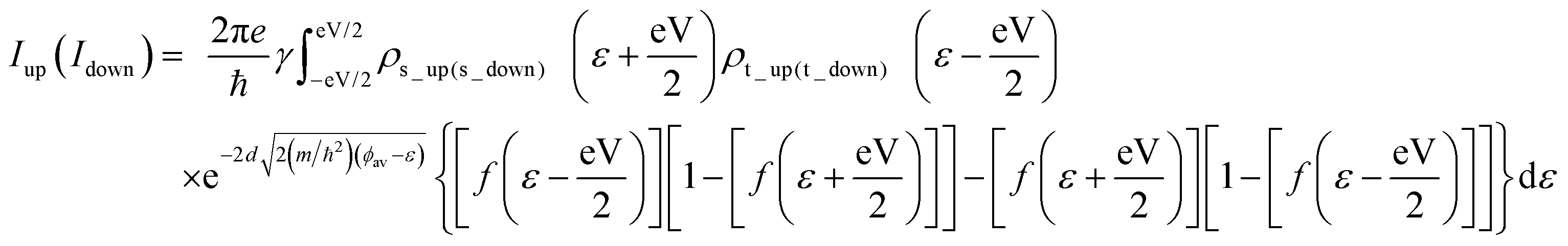
A model setup of scanning tunneling microscopy (STM) was used to calculate the transverse electron transport properties of the doped monolayers supported on the Au substrate with the distance of 3 Å from the monolayer to the substrate, a value obtained in our earlier study on Si-doped BN.8 The tip is considered to be separated from the in-plane BN monolayer by a vacuum barrier width of 5 Å, mimicking a non-bonded tip configuration for the STM measurements. The spin-polarized electron tunneling current through the monolayer between the substrate and the tip was calculated based on the Bardeen, Tersoff and Hamann (BTH) formalism, where the spin-polarized electron tunneling current between two electrodes can be written as I = Iup + Idown, where the Iup and Idown are the contributions from spin-up and spin-down states. In the low-bias limit, Iup(Idown) can be calculated at finite temperature as follows:26
 | (1) |
In our calculations, the cap configuration of the tip was simulated by an icosahedral Au13 cluster, and the supercell was chosen in such a way that the Au(111) substrate surface is commensurate with the h-BN lattice. A (4 × 6) supercell consisting of 24 B and 24 N atoms was used for the doped BN monolayer, and a four-layer slab with 18 atoms per layer was used to simulate the Au(111) substrate in our calculations.8
3. Results and discussion
3.1. Equilibrium structure and stability
Two types of sites were chosen for dopants in the h-BN lattice including (i) a site with 3-fold coordination, where a C or Ge atom replaced either B or N, and (ii) a site with 4-fold coordination where a C or Ge atom goes into a divacancy site formed by removing neighboring B and N atoms in the 2D lattice. Fig. 1 shows the equilibrium configurations of 3-fold coordinated dopants (i.e. CB, CN, GeB and GeN) and 4-fold coordinated dopants (i.e. CBN and GeBN) in the h-BN lattice. The corresponding structural parameters are listed in Tables 1 and 2.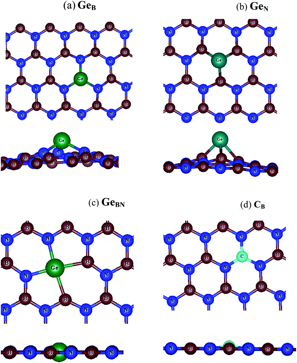 | ||
| Fig. 1 Top and side views of C and Ge doped BN monolayers (B-red atom, N-blue atom, Ge-green atom, and C-dark sky color atom): (a) 3-fold coordinated GeB, (b) 3-fold coordinated GeN, (c) 4-fold coordinated GeBN (CBN is equivalent with C in place of Ge), and (d) a nearly planar structure with a small protrusion of CB (CN is equivalent). | ||
| Dopant | Configuration | Nearest-neighbor distance (RGe) (Å) | B-rich formation energy (eV) | N-rich formation energy (eV) | Magnetic moment (μB) |
|---|---|---|---|---|---|
| 3-Fold Ge at B-site (GeB) | In-plane | 1.85 | 7.9 | 4.6 | 1.0 |
| Out of plane | 1.50 | 4.6 | 1.3 | 1.0 | |
| 3-Fold Ge at N-site (GeN) | In-plane | 2.10 | 7.7 | 11.0 | 1.0 |
| Out of plane | 1.98 | 3.6 | 7.0 | 1.0 | |
| 4-Fold Ge (GeBN) | In-plane (Ge-B) | 2.08 | 6.4 | 6.4 | 0.0 |
| In-plane (Ge-N) | 1.88 | ||||
| Dopant | Configuration | Nearest-neighbor distance (RC) (Å) | B-rich formation energy (eV) | N-rich formation energy (eV) | Magnetic moment (μB) |
|---|---|---|---|---|---|
| 3-Fold C at B-site (CB) | In-plane | 1.41 | 11.9 | 8.6 | 1.0 |
| Out of plane | ∼0 | 3.2 | −0.1 | 1.0 | |
| 3-Fold C at N-site (CN) | In-plane | 1.51 | 11.7 | 15.0 | 1.0 |
| Out of plane | ∼0 | −0.3 | 3.0 | 1.0 | |
| 4-Fold C (CBN) | In-plane (C-B) | 2.19 | 7.3 | 7.3 | 0.0 |
| In-plane (C-N) | 1.46 | ||||
In the equilibrium configuration, CB is connected to the three nearest N atoms with equal C–N bond length of ∼1.41 Å. On the other hand, C substituting N is connected to the three nearest B atoms with equal C–B bond length of ∼1.51 Å. Note that the calculated bond length for the pristine BN monolayer is 1.45 Å. We find that C-doped configurations prefer the slightly convex geometry configuration which is consistent with the previous investigation.21 There is a more pronounced convex geometry around Ge which protrudes 1.5 and 1.98 Å from the monolayer plane for GeB and GeN, respectively (Fig. 1). The in-plane symmetry of the monolayer is broken and Ge forms a tetrahedral structure with three neighboring N or B atoms taking a sp3-like hybridization. For the case of GeB, the dopant is connected to the three nearest N atoms with equal Ge–N bond length of ∼1.85 Å. On the other hand, Ge substituting N is connected to the three nearest B atoms with equal Ge–B bond length of ∼2.10 Å. Taking into account the Si doping case,8 as an isoelectronic system, we can note a trend in the increase of the nearest neighbor bond length with the increase of the core charge screening, which is highest in Ge and lowest in C pseudopotentials. Short C–N and C–B bonds allow the accommodation of C dopants in almost planar configurations.
The 4-fold coordinated CBN and GeBN prefer an in-plane configuration in which C and Ge take sp2d-like hybridization. They form four in-plane bonds with neighboring B and N atoms and show similar characteristics to the Si doped BN.8 In this case, the Ge substituting divacancy of B and N is connected to the two nearest B and N atoms, respectively, with unequal bond lengths of ∼2.08 Å (Ge–B) and ∼1.88 Å (Ge–N), while the C substituting divacancy of B and N is connected to the two nearest B and N atoms, respectively, with bond lengths of ∼2.19 Å (C–B) and ∼1.46 Å (C–N).
In order to investigate the stability of the dopant in the lattice, we define the formation energy Ef to represent the case of nC/Ge germanium or carbon atoms substituting nB boron and nN nitrogen atoms (note nB + nN = nGe/C for single-site doping only). Ef can then be formulated as presented elsewhere.8 We have chosen μBN as the total energy per B–N pair in a pristine h-BN monolayer. μGe/C is chosen to be the cohesive energy per atom of the Ge bulk (Ecoh = −3.85 eV) and graphite bulk (Ecoh = −7.37 eV).27 The choice of μB and μN is given by the growth conditions to be considered during the doping process. In the N-rich environment, μN is set to half of the binding energy of an N2 molecule (Eb = −9.9 eV).28 In the B-rich environment, μB is set to the cohesive energy of the α-boron bulk material (Ecoh = −5.81 eV29).
The calculated formation energies are also given in Table 1 and 2 for Ge and C atom doped h-BN monolayers, respectively. The formation energy of the 4-fold CBN and GeBN does not vary with μB due to the imposed constraint of the equilibrium conditions.16 Thus, the formation of GeB is preferred over GeN and GeBN in the BN monolayer under a N-rich environment, while GeN is preferential to B-rich conditions. Furthermore, it is clear that the formation of CB is preferred over CN and CBN in the BN monolayer under an N-rich environment, while CN is also preferential under B-rich conditions (Table 2).
Note that the positive formation energy indicates that the substitutional doping requires energy to be available, since the doping process occurs under thermodynamical equilibrium with the atomic reservoirs. However, even if such conditions may not be applicable to a particular experiment required for doping the monolayer, changes in the formation energies as calculated here serve as an implication of how difficult it will be to substitute a B or N atom by a Ge or C atom in the monolayer. It is to be noted that a C-doped BN monolayer was recently synthesized.11
3.2. Electronic properties
Fig. 2 and 3 show the calculated band structures of pristine and doped BN monolayers, respectively. The top of the valence band of pristine h-BN is primarily composed of N-p states, while the bottom of the conduction band is mainly constituted by B-p states.30 A direct gap of 4.5 eV is calculated near the K point. This agrees well with the previous theoretical studies reporting the gap to be 4.6 eV,11 4.4 eV,31 and 4.75 eV.21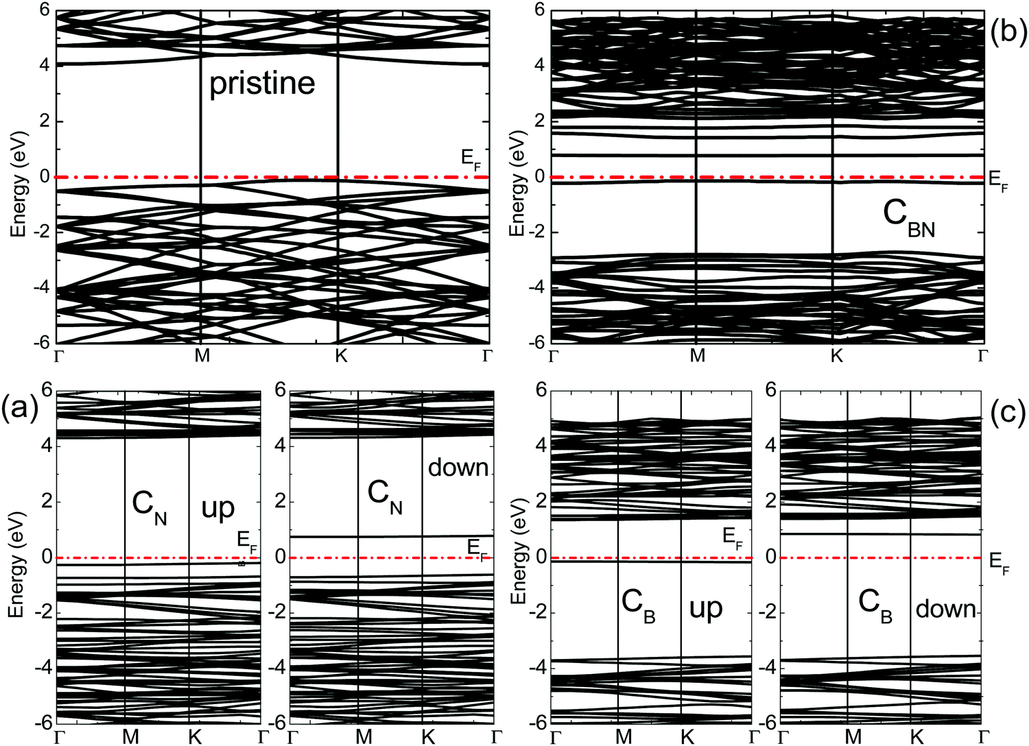 | ||
| Fig. 2 The calculated band structures of pristine and C doped BN monolayers: (a) CN, (b) CBN, and (c) CB; ‘up’ and ‘down’ refer to the spin-up and spin-down components of the band structure. The dotted line represents the Fermi energy (EF) of the system. | ||
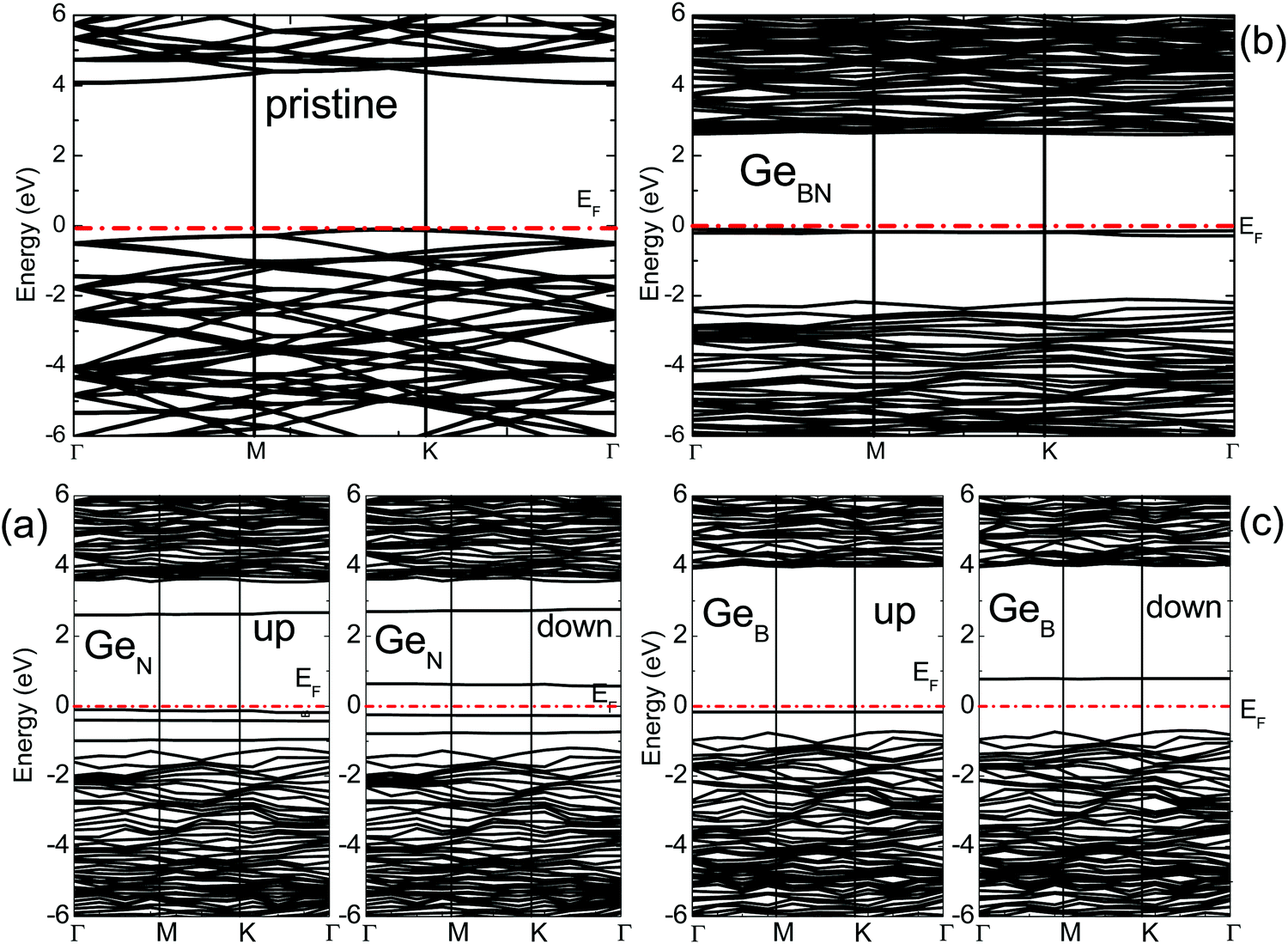 | ||
| Fig. 3 The calculated band structures of pristine and doped BN monolayers: (a) GeN, (b) GeBN, and (c) GeB; ‘up’ and ‘down’ refer to the spin-up and spin-down components of the band structure. The dotted line represents the Fermi energy (EF) of the system. | ||
The spin resolved band structures of the C and Ge doped monolayers (Fig. 2 and 3) retain most of the features in the valence and conduction bands as compared to the pristine monolayer. Appearance of the so-called mid-gap states suggests that the change in the electronic structure induced by doping is likely to be localized in the vicinity of C and Ge atoms. This is confirmed by analysis of the density of states (DOS) revealing that the mid-gap state primarily originates from the C-p states and Ge-s, Ge-p, as well as Ge-d states, for the C- and Ge-doped BN monolayer, respectively (Fig. 4 and 5 and ESI,† Fig. S1–S6).
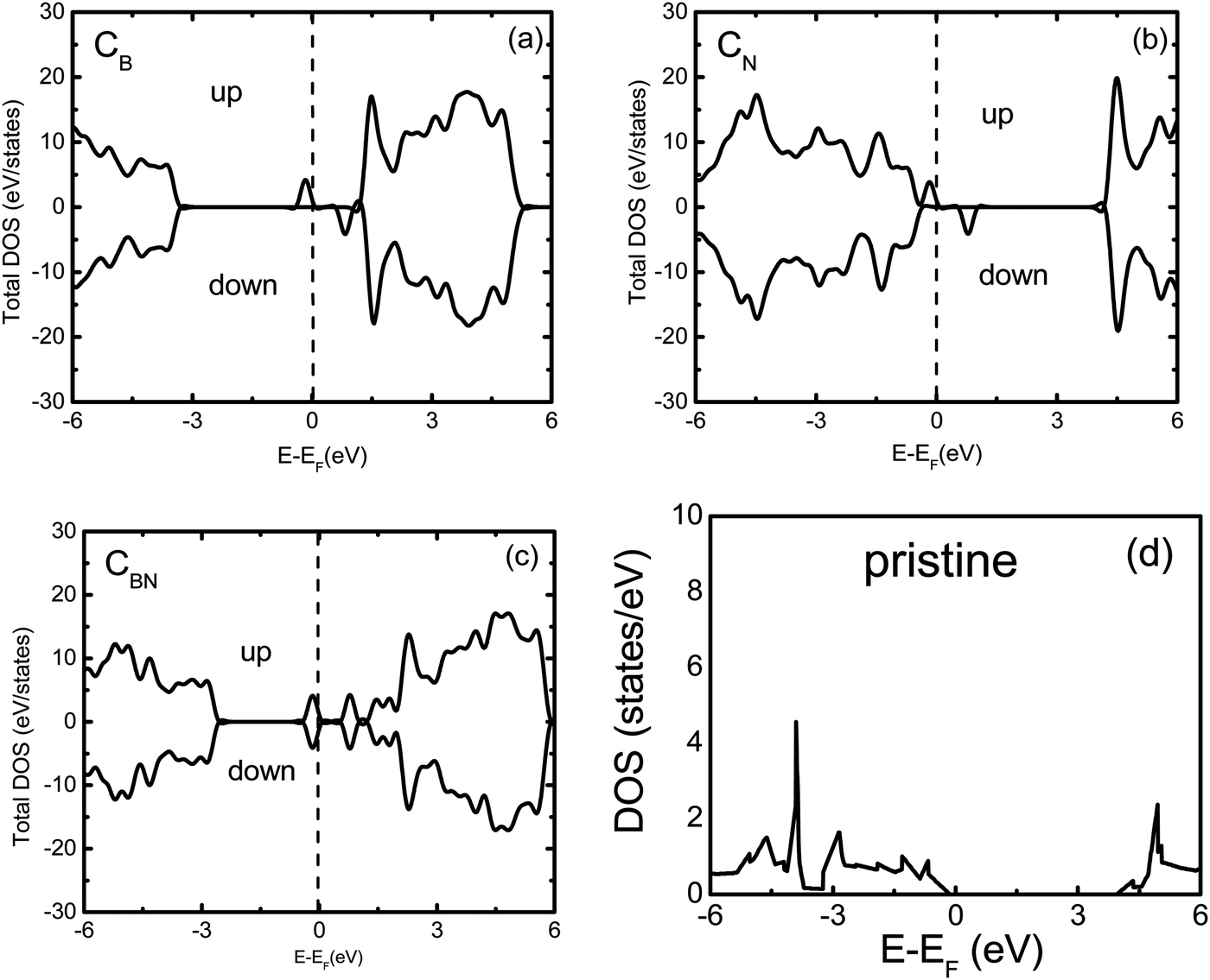 | ||
| Fig. 4 Total density of states of pristine and doped BN monolayers: (a) CB, (b) CN, (c) CBN and (d) a pristine BN monolayer; ‘up’ and ‘down’ refer to the spin-up and spin-down components, and zero is aligned to the Fermi energy (EF) of the system. | ||
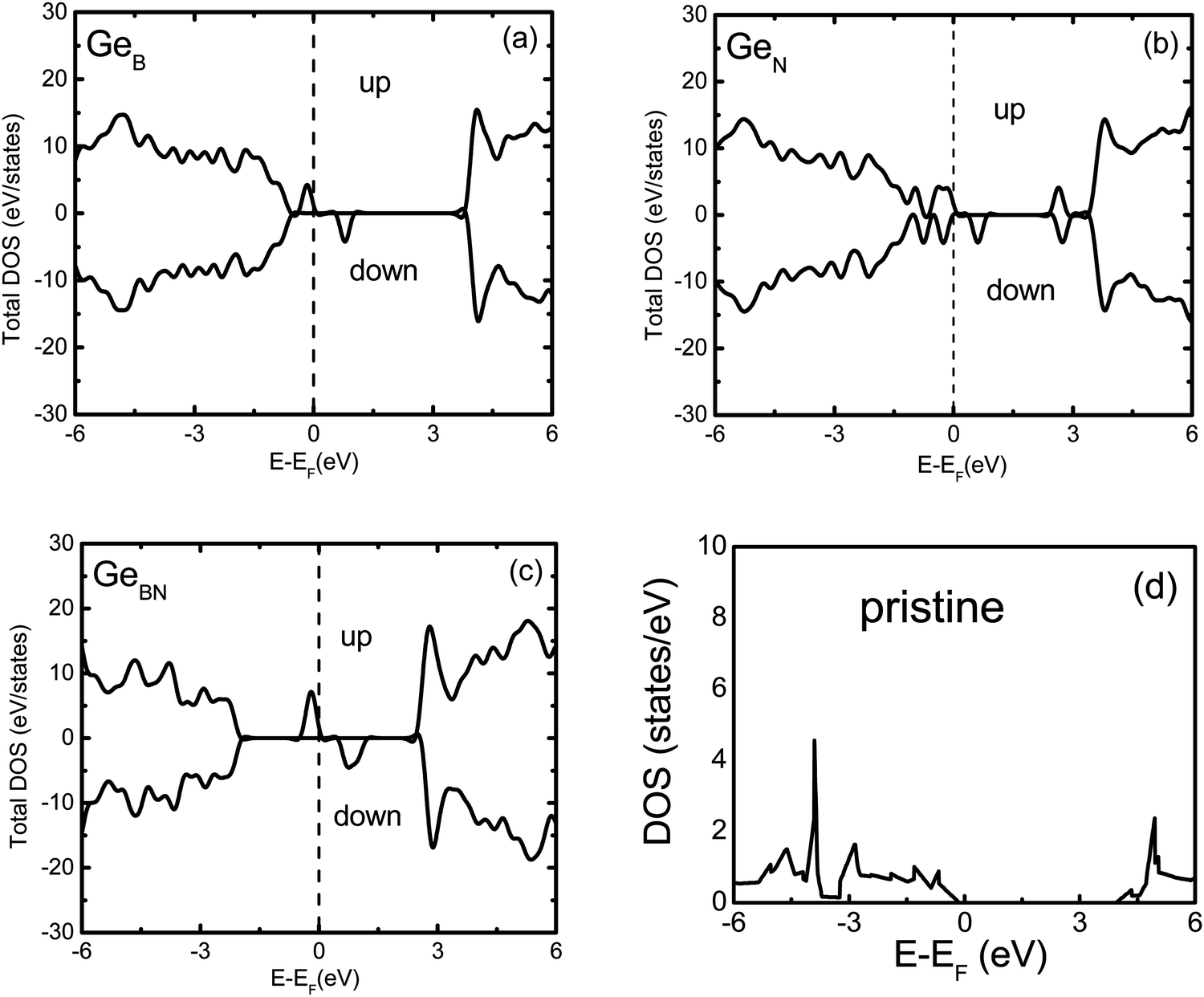 | ||
| Fig. 5 Total density of states of pristine and doped BN monolayers: (a) GeB, (b) GeN, (c) GeBN and (d) a pristine BN monolayer; ‘up’ and ‘down’ refer to the spin-up and spin-down components, and zero is aligned to the Fermi energy (EF) of the system. | ||
The mid-gap states for GeB are located 0.2 eV and 0.75 eV above the valence band maximum (VBM) for the spin-up and spin-down electrons, respectively. This is somewhat similar to the CB case, except that the valence and conduction band states in GeB are shifted toward higher energies. As the dopant Ge atom relaxes from an in-plane to an out-of-plane configuration, its gap state, as a donor state, splits from the conduction band and moves down in energy. The spin-up orbital becomes occupied, while the spin-down orbital remains unoccupied, leading to the spontaneously induced magnetization in the monolayer with a net magnetic moment of 1 μB per dopant (Tables 1 and 2).
Four distinct mid-gap states can be found within the band gap of GeN, which are nearly dispersion-less (Fig. 3). Three of them are closer to each other and located about 0.25 eV and 0.75 and 1.0 eV, respectively, above the VBM for the spin-up case, while the fourth state is lying at 3.75 eV above the VBM. In the spin-down case, one of the lower three states shifts up above the Fermi level. The lower two levels are located about 0.5 eV and 1.0 eV above the VBM, while the remaining two states are at 1.75 and 4.0 eV above the VBM, also leading to magnetization. In the case of CN, the top mid-gap state appears at approximately the same positions regarding the Fermi level as in the CB and GeB cases (Fig. 2). Analysis of atom and orbital projected DOS (ESI,† Fig. S1, S2, S4 and S5) suggests that the occupied mid-gap states are composed of C, Ge, N and B orbitals for both C and Ge doped BN monolayers. Relative positions of the C dopant levels with respect to the VBM and CBM in both CB and CN cases agree well with the DFT-PBE results.21
Two partially degenerate gap states are seen in the band gap (Fig. 3) of GeBN and are both occupied states. The gap states are a hybridization of Ge-p, Ge-d and B-p states of the doped monolayer. No spontaneous magnetization was found in this case, as the contributions from spin-up and spin-down states are almost the same (ESI,† Fig. S6). The situation for CBN is interesting in that one distinct state near the Fermi level is occupied (primarily consisting of C-p orbitals) and three (C and B hybridized) states split from the CBM are unoccupied with equal spin contributions leading also to the non-magnetic state. In C doped BN, C and B orbitals form most of the unoccupied band located near the CBM (ESI,† Fig. S3), while in the case of Ge doped BN, Ge and B unoccupied bands are hybridized with N-p states. Different electronic properties originating from the diverse electronic bonding and positions of the dopant mid-gap states can be used as precursors to anticipate different transport properties of C and Ge doped BN monolayers.
3.3. Electronic transport properties
Fig. 6 shows the conventional STM setup which was used to calculate the tunneling current through the doped BN monolayer deposited on the Au(111) substrate. The calculated tunneling currents associated with pristine and doped BN monolayers are plotted in Fig. 7 over the range of external bias between −0.5 V and +0.5 V. We define the bias to be positive when the gold substrate and the BN monolayer are connected to a positive potential and when electrons tunnel from the tip to the monolayer, as illustrated in Fig. 6. The process of electron tunneling is observable as a current from the occupied states of one side to the unoccupied states of another side of the STM. The direction of current, thus, essentially depends on the choice of the bias. The tunneling current will crucially depend on the filled and unfilled electron states near the Fermi energy. Also, the current will depend on the tip-monolayer distance, but will not, however, influence the trends in the I–V characteristics predicted below.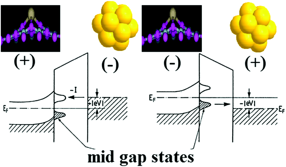 | ||
| Fig. 6 A schematic illustration of the model STM setup for calculations of the electron transport in the h-BN monolayer deposited on the Au substrate (Ge/C-grey atom, N-light blue atom, B-pink atom, and Au- golden atom). The cap of the tip is simulated by the gold cluster (Au13). | ||
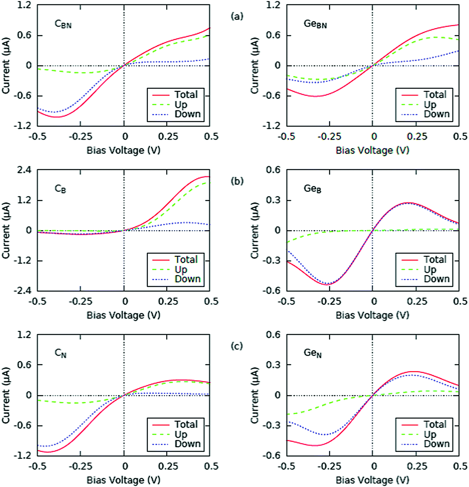 | ||
| Fig. 7 The current–voltage characteristics of the doped BN monolayers: (a) CBN and GeBN, (b) CB and GeB and (c) CN and GeN; ‘up’ and ‘down’ refer to the spin-up and spin-down components. | ||
For the pristine monolayer, the threshold voltage is about 5 meV and one can find an approximately linear positive relationship of the tunneling current vs. voltage over either a B or N atom. Also, the current through N (≈0.1 μA at 0.5 V) is significantly higher than that through B (≈0.02 μA at 0.5 V). This result follows from the fact that N states dominate the DOS of pristine BN near the Fermi level.
C and Ge doped BN monolayers exhibit prominent electron transport properties which are displayed in Fig. 7. First, the tunneling current over the dopants Ge and C is higher than that over the host atoms as was the case with the Si-doped BN monolayer.8 Second, an asymmetric response of the transverse tunnel current, sampled at the Ge and C atoms is predicted. For GeB and GeN, the magnitude of tunneling current under the negative bias of −0.5 V (with electrons tunneling from the monolayer to the tip) is higher than that under the positive bias of +0.5 V (with electrons tunneling from the tip to the monolayer), while the case is reversed for GeBN. More noticeable, however, are the regions of negative resistance occurring at high negative and positive biases. This behavior has led us to investigate the differential conductance as discussed below.
The case of C doped BN presents some more interesting features. For CBN and CN the magnitude of tunneling current under the negative bias is higher than that under the positive bias. For CB, however, the application of the external bias increases the current significantly. The current under the negative bias is lower than that under the positive one, but what is even more important is that it has a value of almost zero, while for the positive bias it is around 2.2 μA. The ratio of the currents, I(+0.5 V)/I(−0.5 V), in this case is noticeably large (nearly ∼22) for CB as represented in Fig. 7. The spin-up component in CB (similar to GeB for positive bias) is actually zero for negative bias. We could correlate this to the spin diodes and spin filtering combined with the perfect diode effect as effects contributing to the spin-polarized transport properties of doped BN. Other cases could also be considered, with appropriate modifications, for applications in spin valve systems, especially GeB, which has an almost zero spin-up current for positive bias or CBN, which has a low spin-down current for positive bias and low spin-up current for negative bias.
The spin-polarized properties, predicted on the theoretical basis, present the realistic promise of application of a doped BN monolayer as a switch component in nanoelectronic devices. Furthermore, it is interesting to point out that one can distinguish between different substitutional sites by evaluating their STM images under positive and negative biases. Larger variations will be observed in monovacancy site BN (current ratios larger than 3) and less variations will be observed in divacancy site BN (CBN and GeBN with current ratios around 1). Negative resistance regions are not as prominent as in the Ge doping case.
It is important to note that the tunneling current is an integration of the convolution of DOS of the tip and the sample. To fully understand the role of substituting the BN monolayer with C or Ge atoms, we now turn again to the changes in the electronic structure upon doping. It is apparent that a large tunneling current over the Ge and C atoms is due only to the induced gap states stemming from the doping process in the monolayer (Fig. 4 and 5 along with the ESI,† Fig. S1–S6). The gap states which appear near the Fermi level constitute the major tunneling “channels” for the electrons under the applied bias. These states are distributed asymmetrically in the positive and negative energies around the Fermi level, so the tunneling currents associated with the dopant Ge and C also show asymmetric features under positive and negative biases. In addition, the mentioned linear increase of the tunneling current with increasing applied bias is most probably due to the finite DOS of the simulated Au13 cluster tip at the Fermi level (ESI,† Fig. S7).
The effect of the Au substrate is also considered (ESI,† Fig S8–S11). Projected DOS shows that the additional states at and around the Fermi level are due to the gold substrate and the doped BN monolayer. A certain degree of hybridization is noticed with the electron states belonging to the doping elements. The contribution of the doping elements readily falls down toward the Fermi level. Energy dependence of this behavior directly influences the behavior of the tunneling current, inducing the decrease of its magnitude toward the higher bias values. Exceptions are divacancy BN monolayers in the regime of positive bias, where the current increases steadily. The finite DOS at the Fermi level is a result of the interaction between the doped BN monolayer and the Au substrate, which broadens the introduced mid-gap states over the Fermi level. This consequently leads to the increase of the tunneling current.
Distinct features of the mid-gap states in the doped monolayers also lead to the resonant tunneling phenomena, where the small negative differential resistance (NDR) effect32–34 is predicted, as reflected in the differential conductance characteristic (Fig. 8). Differential conductance has negative values under about −0.3 V of the negative bias voltage in all considered cases of doped BN. In monovacancy BN it also occurs for the positive bias. The same effect has been noted in SiN doped BN, but not in SiB.8 The reason is the quasi-linear behavior of I–V characteristics in SiB. In these regimes the negative values are a consequence of the mismatch between the DOS peaks of the Au tip and the mid-gap states of the doped BN monolayer deposited on the Au substrate. When this mismatch occurs, the tunneling probability drops strongly as a result of the fact that the bias voltage reached the energy at which the tunneling is prohibited. The correspondence between the NDR peak and the mid-gap states, thus, provides a useful tool for tailoring the transport properties in semiconducting materials at the nanoscale.
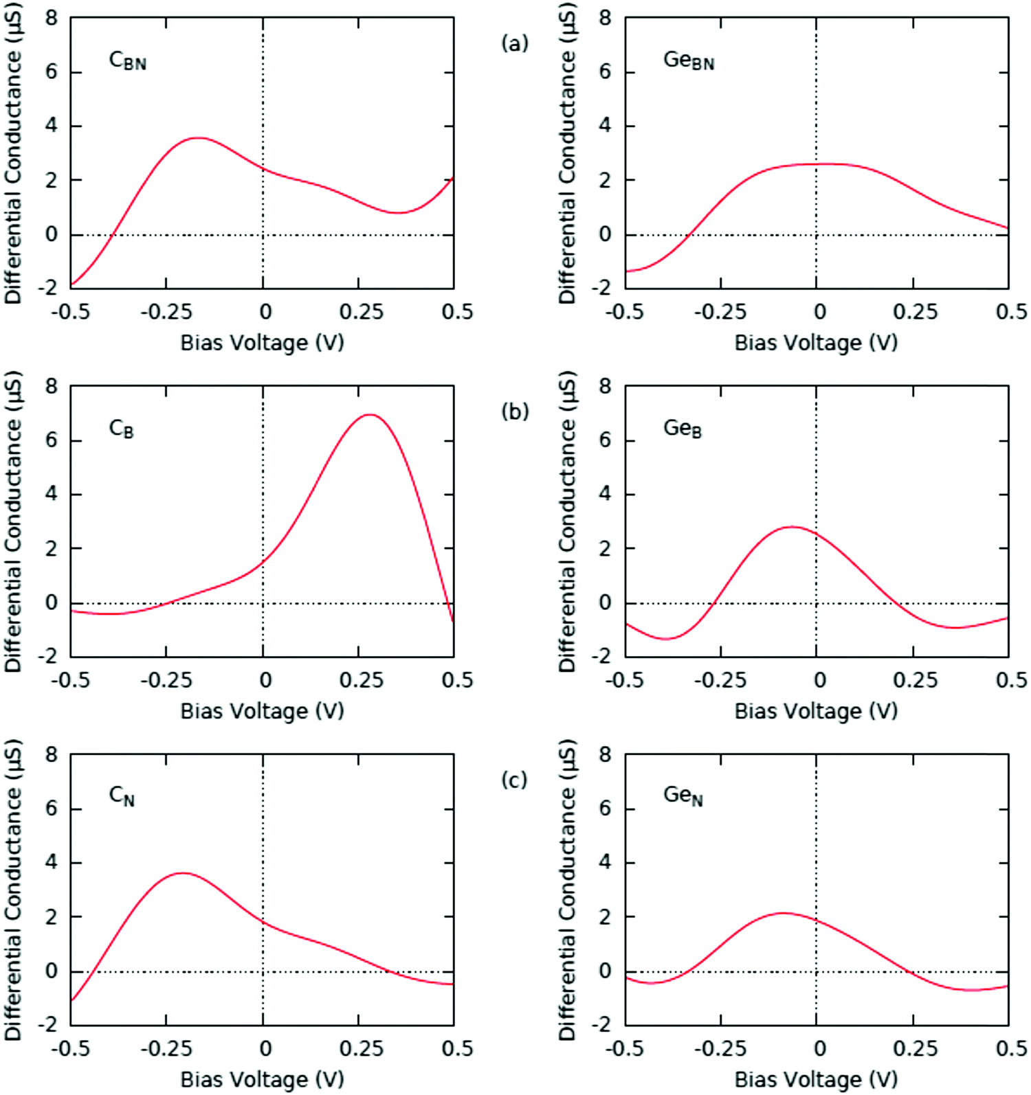 | ||
| Fig. 8 The calculated differential conductance curve of the doped BN monolayers; (a) CBN and GeBN, (b) CB and GeB and (c) CN and GeN. | ||
The simulated STM images generated from the position-projected tunneling currents are shown in Fig. 9. The location of the Ge and C atoms is visible in all cases, and almost each case can be clearly discerned from the other. Comparison of the STM images of the Ge doped BN monolayer reveals that the elevation of the doping atoms above the monolayer plane (GeB and GeN) has a more dominant role than the atom type in influencing the STM image height. A similar effect was noticed in Si doped BN.8 Comparing the three cases of C doped BN, on the other hand, one can distinguish the emphasizing role of the DOS of the doping element at the Fermi level, as in the CB case the C-p states have larger DOS contribution than in CN or CBN cases. The 4-fold coordination can be slightly discerned as the STM image elongates in the bonding directions. This effect is not easily noticed in the 3-fold coordinated configurations. Further comparison of these results with the ones for Si doped BN provides additional insight into the effectiveness of STM imaging of different doped monolayers. We can inductively deduce that a similar behavior, the increase of the image height with the increase of atomic number, will be observed in other monolayer systems doped with isoelectronic atoms.
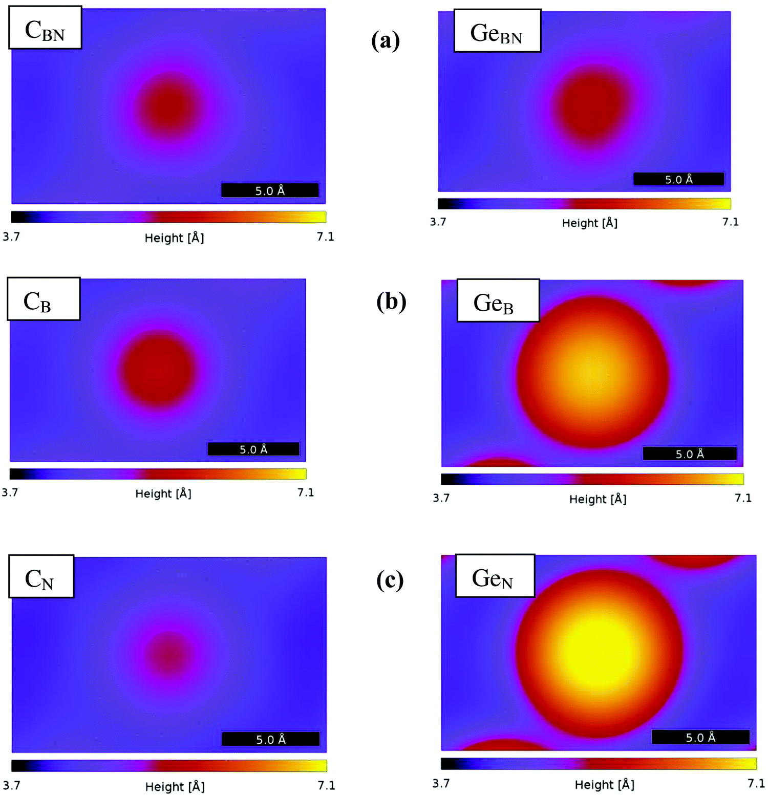 | ||
| Fig. 9 The STM images at constant current (100 nA, 100 mV) of doped BN monolayers: (a) CBN and GeBN, (b) CB and GeB, and (c) CN and GeN. | ||
4. Summary
In summary, we have investigated the stability and electronic properties of C and Ge doped BN monolayers in the framework of density functional theory. The calculated results indicate that the dopant substituting B atom is preferred over the dopant substituting N atom for N-rich conditions. The unpaired electron associated with the CB or GeB and CN or GeN induces a magnetic moment in the doped BN monolayer, and the spin is primarily located mostly on the Ge-p/d orbitals and C-p orbitals in the lattice. The 4-fold CBN and GeBN configurations, however, do not induce magnetism, as Ge and C dopants take a sp2d and sp3 type of hybridization, respectively in their in-plane monolayer configurations.We find that dopants induce mid-gap states near the Fermi level of the pristine monolayer which have a profound effect on the electronic band structure and electron transport properties. The transverse tunnel current through the doped monolayer has a significantly higher magnitude than through the pristine monolayer. The current–voltage curves sampled at the dopant sites exhibit remarkable asymmetric response due to the polarity of the bias voltage. Most interestingly, an almost perfect diode effect is predicted for the case of CB allowing the applications of doped BN monolayers in electronic devices with the sizes on the scale of nanometers. This is important as their small size enables denser packing of electronic components. Besides, a spin filtering effect is observed in CB, GeB and CN for various bias voltage ranges, while other cases show promise for spin valve system applications under specific modifications. The basic task would be to find a way to increase the value of non-zero current while keeping the zero current for the reverse spin. This property could pave the way for doped BN into the area of spintronics as a component in spin valve systems, magnetic random-access-memories (MRAM), magnetic sensors or spin based logic gates.
The doped monolayers also exhibit a negative differential resistance behavior in their current–voltage characteristics. This behavior opens up possible applications in electronic oscillators, amplifiers or switching circuits. Without doubt it can be realized in other similar systems coupled to the STM experimental setup. Furthermore, our simulations suggest that the monolayer morphology can be sampled with STM. The distribution of the doping elements can be controlled using STM, as the calculated position-projected tunneling currents provide the STM images discerning the site-dependence of the Ge and C atoms in the 2D BN monolayer.
Conflicts of interest
There are no conflicts to declare.Acknowledgements
Helpful discussions with Dr Douglas Banyai are acknowledged, and SKG acknowledges the Fulbright fellowship and hospitality of Michigan Technological University. RAMA and Superior, high performance computing clusters at Michigan Technological University, were used in obtaining results presented in this paper. Helpful support from Dr S. Gowtham is gratefully acknowledged.References
- L. Camilli, E. Sutter and P. Sutter, Growth of two-dimensional materials on non-catalytic substrates: h-BN/Au (111), 2D Mater., 2014, 1(2), 025003 CrossRef.
- A. Ismach, P. Mende, A. Dolocan, R. Addou, S. Aloni, R. Wallace, R. Feenstra, R. Ruoff and L. Colombo, Carbon-Assisted Chemical Vapor Deposition of Hexagonal Boron Nitride, 2D Mater., 2017, 4, 025117 CrossRef.
- S. Sonde, A. Dolocan, N. Lu, C. Corbet, M. J. Kim, E. Tutuc, S. K. Banerjee and L. Colombo, Ultrathin, wafer-scale hexagonal boron nitride on dielectric surfaces by diffusion and segregation mechanism, 2D Mater., 2017, 4(2), 025052 CrossRef.
- K. S. Novoselov, D. Jiang, F. Schedin, T. J. Booth, V. V. Khotkevich, S. V. Morozov and A. K. Geim, Two-Dimensional Atomic Crystals, Proc. Natl. Acad. Sci. U. S. A., 2005, 102, 10451–10453 CrossRef CAS PubMed.
- G.-H. Lee, Y.-J. Yu, X. Cui, N. Petrone, C.-H. Lee, M. S. Choi, D.-Y. Lee, C. Lee, W. J. Yoo and K. Watanabe, Flexible and Transparent MoS2 Field-Effect Transistors on Hexagonal Boron Nitride-Graphene Heterostructures, ACS Nano, 2013, 7, 7931–7936 CrossRef CAS PubMed.
- C. R. Dean, A. F. Young, I. Meric, C. Lee, L. Wang, S. Sorgenfrei, K. Watanabe, T. Taniguchi, P. Kim, K. L. Shepard and J. Hone, Boron Nitride Substrates for High-Quality Graphene Electronics, Nat. Nanotechnol., 2010, 5(10), 722–726 CrossRef CAS PubMed.
- J. Qi, X. Qian, L. Qi, J. Feng, D. Shi and J. Li, Strain-Engineering of Band Gaps in Piezoelectric Boron Nitride Nanoribbons, Nano Lett., 2012, 12, 1224–1228 CrossRef CAS PubMed.
- S. K. Gupta, H. He, D. Banyai, M. Si, R. Pandey and S. P. Karna, Effect of Si Doping on the Electronic Properties of BN Monolayer, Nanoscale, 2014, 6, 5526–5531 RSC.
- G. C. Loh, R. Pandey, Y. K. Yap and S. P. Karna, MoS2 Quantum Dot: Effects of Passivation, Additional Layer, and h-BN Substrate on Its Stability and Electronic Properties, J. Phys. Chem. C, 2015, 119, 1565–1574 CAS.
- X. Qian, Y. Wang, W. Li, J. Lu and J. Li, Modelling of stacked 2D materials and devices, 2D Mater., 2015, 2(3), 032003 CrossRef.
- Z. Zhang, X. Liu, J. Yu, Y. Hang, Y. Li, Y. Guo, Y. Xu, X. Sun, J. Zhou and W. Guo, Tunable Electronic and Magnetic Properties of Two-Dimensional Materials and Their One-Dimensional Derivatives, Comput. Mol. Biosci., 2016, 6, 324–350 CrossRef CAS PubMed.
- Y. Lin, T. V. Williams, W. Cao, H. E. Elsayed-Ali and J. W. Connell, Defect Functionalization of Hexagonal Boron Nitride Nanosheets, J. Phys. Chem. C, 2010, 114, 17434–17439 CAS.
- L. Zhao, M. Levendorf, S. Goncher, T. Schiros, L. Pálová, A. Z. Khosousi, K. T. Rim, C. Gutiérrez, D. Nordlund, C. Jaye, M. Hybertsen, D. Reichman, G. W. Flynn, J. Park and A. N. Pasupathy, Local Atomic and Electronic Structure of Boron Chemical Doping in Monolayer Graphene, Nano Lett., 2013, 13, 4659–4665 CrossRef CAS PubMed.
- J.-H. Yang, D. Kim, J. Hong and X. Qian, Magnetism in Boron Nitride Monolayer: Adatom and Vacancy Defect, Surf. Sci., 2010, 604, 1603–1607 CrossRef CAS.
- R.-F. Liu and C. Cheng, Ab Initio Studies of Possible Magnetism in a BN Sheet by Nonmagnetic Impurities and Vacancies, Phys. Rev. B: Condens. Matter Mater. Phys., 2002, 76, 014405 CrossRef.
- X. Wei, M.-S. Wang, Y. Bando and D. Golberg, Electron-Beam-Induced Substitutional Carbon Doping of Boron Nitride Nanosheets, Nanoribbons, and Nanotubes, ACS Nano, 2011, 5, 2916–2922 CrossRef CAS PubMed.
- X. Wei, M.-S. Wang, Y. Bando and D. Golberg, Post-Synthesis Carbon Doping of Individual Multiwalled Boron Nitride Nanotubes via Electron-Beam Irradiation, J. Am. Chem. Soc., 2010, 132, 13592–13593 CrossRef CAS PubMed.
- L. Liu, T.-K. Sham and W. Han, Investigation on the Electronic Structure of BN Nanosheets Synthesized Via Carbon-Substitution Reaction: The Arrangement of B, N, C and O atoms, Phys. Chem. Chem. Phys., 2013, 15, 6929–6934 RSC.
- J.-X. Zhao and B.-Q. Dai, DFT Studies of Electro-Conductivity of Carbon-Doped Boron Nitride Nanotube. Mat, Chem. Phys., 2004, 88, 244–249 CAS.
- C. Huang, C. Chen, M. Zhang, L. Lin, X. Ye, S. Lin, M. Antonietti and X. Wang, Carbon-Doped BN Nanosheets for Metal-Free Photoredox Catalysis, Nat. Commun., 2015, 6, 7698–7705 CrossRef PubMed.
- N. Berseneva, A. Gulans, A. V. Krasheninnikov and R. M. Nieminen, Electronic Structure of Boron Nitride Sheets Doped With Carbon From First-Principles Calculations, Phys. Rev. B: Condens. Matter Mater. Phys., 2013, 87, 035404 CrossRef.
- R. Wang, D. Zhang and C. Liu, The Germanium-Doped Boron Nitride Nanotube Serving as a Potential Resource for the Detection of Carbon Monoxide and Nitric Oxide, Comput. Mater. Sci., 2014, 82, 361–366 CrossRef CAS.
- J. Wu and W. Zhang, Magnetism in Germanium-Doped Boron-Nitride Nanotubes, Chem. Phys. Lett., 2008, 457, 169–173 CrossRef CAS.
- J. P. Perdew, K. Burke and M. Ernzerhof, Generalized Gradient Approximation Made Simple, Phys. Rev. Lett., 1996, 77, 3865–3868 CrossRef CAS PubMed.
- G. Kresse and J. Furthmuller, Efficient Iterative Schemes for Ab Initio Total-Energy Calculations Using a Plane-Wave Basis Set, Phys. Rev. B: Condens. Matter Mater. Phys., 1996, 54, 11169–11186 CrossRef CAS.
- J. Tersoff and D. R. Hamann, Theory and Application for the Scanning Tunneling Microscope, Phys. Rev. Lett., 1983, 50, 1998–2001 CrossRef CAS.
- http://cmt.dur.ac.uk/sjc/thesis_ppr/node50.html .
- Y. Yan, S. B. Zhang and S. T. Pantelides, Control of Doping by Impurity Chemical Potentials: Predictions for p-Type ZnO, Phys. Rev. Lett., 2001, 86, 5723–5726 CrossRef CAS PubMed.
- K. C. Lau, R. Orlando and R. Pandey, First-Principles Study of Crystalline Bundles of Single-Walled Boron Nanotubes with Small Diameter, J. Phys.: Condens. Matter, 2008, 20, 125202 CrossRef.
- N. Ooi, A. Rairkar, L. Lindsley and J. B. Adams, Electronic Structure and Bonding in Hexagonal Boron Nitride, J. Phys.: Condens. Matter, 2006, 18, 97–115 CrossRef CAS.
- C. Stampfl and C. G. Van de Walle, Density-Functional Calculations for III-V Nitrides Using the Local-Density Approximation and the Generalized Gradient Approximation, Phys. Rev. B: Condens. Matter Mater. Phys., 1999, 59, 5521–5535 CrossRef CAS.
- P. Bedrossian, D. M. Chen, K. Mortensen and J. A. Golovchenko, Demonstration of the Tunnel-Diode Effect on an Atomic Scale, Nature, 1989, 342, 258–260 CrossRef CAS.
- R. L. Carroll and C. B. Gorman, The Genesis of Molecular Electronics, Angew. Chem., Int. Ed. Engl., 2002, 41, 4378–4400 CrossRef PubMed.
- N. J. Tao, Electron Transport in Molecular Junctions, Nat. Nanotechnol., 2006, 1, 173–181 CrossRef CAS PubMed.
Footnotes |
| † Electronic supplementary information (ESI) available. See DOI: 10.1039/c7cp05596j |
| ‡ Current address: Department of Physics, St. Xavier's College, Navrangpura 380009, Ahmedabad, India. |
| This journal is © the Owner Societies 2017 |