
 Open Access Article
 This Open Access Article is licensed under a
 Creative Commons Attribution 3.0 Unported Licence
Voltage dependent admittance spectroscopy for the detection of near interface defect states for thin film solar cells†
Thomas Paul
Weiss
 *,
Shiro
Nishiwaki
,
Benjamin
Bissig
,
Stephan
Buecheler
and
Ayodhya N.
Tiwari
*,
Shiro
Nishiwaki
,
Benjamin
Bissig
,
Stephan
Buecheler
and
Ayodhya N.
Tiwari
Laboratory for Thin Films and Photovoltaics, Empa – Swiss Federal Laboratories for Materials Science and Technology, Überlandstrasse 129, 8600 Dübendorf, Switzerland. E-mail: thomas.weiss@empa.ch
First published on 13th November 2017
Abstract
Recently recorded efficiencies of Cu(In,Ga)Se2 based solar cells were mainly achieved by surface treatment of the absorber that modifies the buffer–absorber interface region. However, only little is known about the electronic properties within this region. In this manuscript voltage dependent admittance spectroscopy is applied to low temperature grown Cu(In,Ga)Se2 based solar cells to detect near interface defect states in the absorber. Under non-equilibrium conditions even defect states close to the interface may cross the Fermi level and hence are detectable using capacitance based measurement methods, in contrast to the case of zero bias conditions. Such defects are of potential importance for understanding device limitations and hence, adequate characterization is necessary. A SCAPS model is developed including a near interface deep acceptor state, which explains the frequency and voltage dependence of the capacitance. Using the same model, also the experimental apparent doping density is explained.
1. Introduction
Among the thin film technologies for photovoltaic applications, Cu(In,Ga)Se2 (CIGS) based solar cells reached highest efficiencies of 22.6%.1 The interface between the absorber and the buffer layer plays a crucial role in achieving high efficiencies. Consequently, various methods were reported to optimize the electronic properties of the interface region such as an In finish after the 3-stage co-evaporation process,2 partial electrolyte treatment,3 KF post-deposition treatment (PDT)4 and recently also PDT with other alkalis.1 However, apart from the n-type doping mechanism of Cd5–10 no investigations were carried out to measure deeper defect states close to the interface, which could considerably contribute to recombination, i.e. electrical active defect states.In this contribution we investigate the electronic properties of the near surface region of the CIGS absorber layer. As a tool we apply admittance spectroscopy to detect deep defect centers. The advantage of admittance spectroscopy is that the measurements can be done on completed devices. Thus, possible effects of the process steps after absorber layer deposition are included. Under equilibrium conditions (dark and zero voltage bias) admittance spectroscopy is only sensitive to defect states, which cross the Fermi level.11 However, as will be shown in this manuscript, this criterion can be used to specifically probe the near surface region by applying a bias voltage to the device. Under these conditions also deep defect levels close to the heterojunction can be probed, which might not cross the Fermi level under equilibrium conditions and thus could not be detected.
The manuscript is structured as follows. In Section 2 a theoretical idea is presented how voltage dependent admittance spectroscopy can provide insights into non-homogeneously distributed defect states. Section 3 describes sample preparation and experimental measurement details. Measurement results are presented and discussed in Section 4. Based on the experimental findings a SCAPS12 model is developed, which incorporates the experimental insights to describe the electronic behavior of the investigated device.
2. Theoretical background
A defect state can only be detected by admittance spectroscopy in equilibrium (dark and zero voltage bias) if the defect state crosses the Fermi level.11 For a homogeneously distributed defect throughout the depth of the absorber this condition is met as long as the energy level of the defect is between EF and EF + qVbi, where EF is the Fermi level and Vbi the built-in voltage. However, defect states which are present only beyond the space charge region (SCR) width will never cross the Fermi level under equilibrium conditions as this region is neutral and no band bending occurs there. On the other hand, defect states located close to the hetero interface might also not cross the Fermi level as the distance of the Fermi level to the valence band maximum is rather large (in the case of an appropriately doped absorber resulting in an inverted front surface layer13). This condition of a near interface defect state under equilibrium conditions is depicted in Fig. 1a.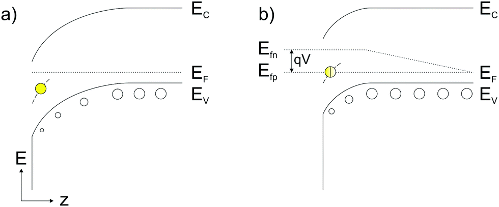 | ||
| Fig. 1 Absorber band diagram under equilibrium conditions (a) and for an applied forward bias voltage (b). A deep defect center has been added to the near surface region. Under equilibrium conditions (a) the defect does not cross the Fermi level and thus cannot be detected by admittance spectroscopy. Applying a forward bias voltage (b) the defect state crosses the hole Fermi level and can be probed by admittance spectroscopy. | ||
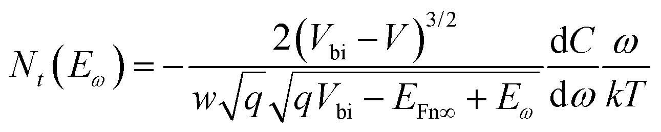
The defect state is located only close to the interface. Within this constrained region the defect state is completely occupied by electrons and cannot be charged/discharged with an additional small ac voltage modulation. Therefore, no capacitance contribution can be observed. Fig. 1b shows this situation under forward bias conditions assuming flat quasi Fermi levels within the SCR. As the bands flatten and the voltage drop across the junction is reduced by the applied bias voltage, the defect level will cross the hole quasi Fermi level and can contribute to the capacitance.14 A similar argument holds for defect states located beyond the SCR, which then can be detected under reverse bias measurements. Decock et al.14 derived an equation, which allows the determination of the defect distribution Nt(Eω) under bias conditions, which reads
 | (1) |
The SCR (for a certain bias voltage) and the built-in voltage can in principle be obtained from a capacitance voltage (C(V)) measurement. However, it needs to be stressed that the interpretation of C(V) measurements is not unambiguous. The apparent doping density from a C(V) measurement might be influenced by deep defect states within the absorber layer15 or a non-homogeneous doping density16,17 as for instance predicted by the Lany–Zunger model.18 The determined built-in voltage might be influenced by interface charge19 and thus cannot be extracted directly from the measurement. As a consequence quantification of a defect state might be difficult but nevertheless a qualitative description is still possible in the sense of the detection of defect states. This information can nevertheless be used as input for device simulations as will be presented in Section 4.2.
Another capacitance contribution, which could show up under forward bias conditions is the diffusion capacitance due to modulation of injected minority carriers.20 For a one-sided junction (n+p) the low frequency diffusion capacitance can be written as20
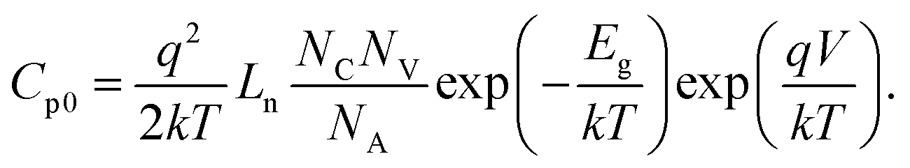 | (2) |
3. Experimental
The measurements in this article are carried out on CIGS based solar cells prepared as follows: the CIGS absorber layer is grown by a low temperature 3-stage process on a Mo/SiO2/soda lime glass (SLG) substrate. The SiO2 layer serves as a barrier for diffusion of impurities from the SLG to the absorber. Details of the absorber growth can be found in ref. 21. After deposition, the absorber layers received an in situ NaF post-deposition treatment (PDT) to increase the acceptor density. Subsequently in situ RbF PDT was applied similar to the previously proposed KF PDT.4,22 PDT with other alkalis than K has already shown to yield similar or even better performances.1 However, this manuscript will not cover the impact of RbF PDT but the insights, which can be gained from voltage dependent admittance spectroscopy in general. After absorber growth and PDT, CdS buffer is deposited by chemical bath deposition. Afterwards an i-ZnO/Al:ZnO window layer is deposited by rf-sputtering and a Ni/Al grid by e-beam evaporation.Current voltage measurements are performed under an ABA solar simulator in 4-probe configuration. Diode parameters are extracted by fitting to a 1-diode model according to Burgers et al.23 Capacitance measurements are carried out as a function of frequency and voltage within a temperature range of 123–323 K by increasing the temperature from low to high temperatures. Prior to cooling, the sample is kept in the dark during night and heated to 50 °C for 1 h to ensure a relaxed state. Voltages are limited to 0.6 V forward bias, which is below the VOC at room temperature. Therefore, especially at low temperatures, no excessive current flow is expected. Device simulations are done using a one-dimensional device simulator SCAPS.12
4. Results and discussion
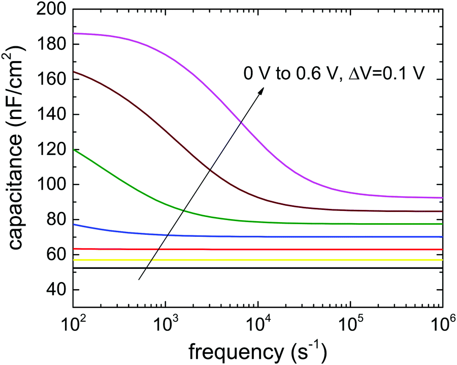
Fig. 2 shows a voltage dependent admittance measurement under equilibrium conditions (a) and under forward bias conditions (b and c) (note the different scales on the ordinate).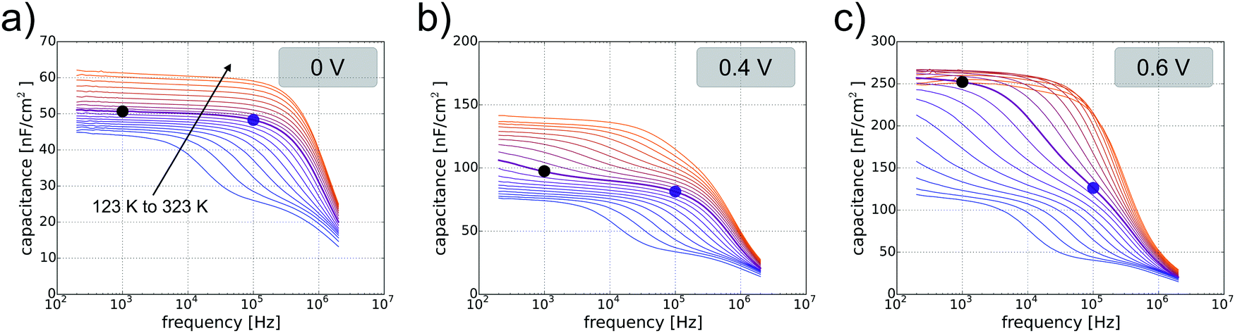 | ||
| Fig. 2 Voltage dependent admittance measurement under equilibrium conditions (a) and under a forward bias of +0.4 V (b) and +0.6 V (c). An additional capacitance step is observed when increasing the applied dc forward bias voltage during the admittance measurement. The thick line indicates the C(f) measurement at the temperature, which is chosen for capacitance voltage analysis. The black and blue dots indicate low and high frequencies used for the analysis of the apparent doping profile. | ||
The measurement under equilibrium conditions (Fig. 2a) shows a capacitance step at low temperatures. This low temperature capacitance step is discussed in the literature.24–27 Recent admittance and temperature dependent IV measurements on similar devices treated under various PDT conditions indicated the capacitance step to be due to a barrier (see also the ESI,† Fig. S4).28,29 Thus, for this manuscript the low temperature capacitance step is assumed to originate from a blocking barrier and will not be discussed in terms of a defect level. As a consequence, the SCR capacitance of the absorber layer is found to be the plateau above the low temperature capacitance step (roughly the value indicated by the blue dot in Fig. 2).25,30
By increasing the dc forward bias during admittance measurements, an additional capacitance step is observed, which becomes more pronounced upon increasing the applied forward bias voltage (Fig. 2b and c). As discussed in Section 2 such a capacitance contribution could arise due to the diffusion capacitance as well as due to a deep defect, which crosses the Fermi level under forward bias conditions (cf.Fig. 1).
Reverse bias measurements were carried out up to −1.5 V dc bias voltage. However, no additional capacitance step is observed. For these conditions the capacitance is flat with respect to frequency and temperature above the low temperature step.
4.1 Diffusion capacitance
To check the influence of the diffusion capacitance we inspect eqn (2). If the diode current is limited by quasi neutral region recombination the diffusion capacitance is proportional to the diode current.20 As can be seen in the ESI,† Fig. S1a, the diode current is limited by the shunt resistance for voltages applied during the admittance measurements (below 0.6 V). Hence, within this voltage range, the diode current increases only linearly with respect to the voltage. However, as the diode quality factor determined from an IV curve is higher than 1 the diode current is not necessarily dominated by quasi neutral region (QNR) recombination but also the SCR and interface (IF) recombination may contribute. Consequently, in comparison to QNR recombination only, the density of injected minority carriers is smaller and therefore also the expected contribution of the diffusion capacitance. Additionally, an upper limit of the diffusion capacitance contribution has been calculated using the low frequency capacitance according to eqn (2). The contribution is plotted for several voltages and as a function of the minority carrier (electrons) diffusion length in the ESI,† Fig. S1b. Other parameters are chosen as Eg = 1.15 eV, NC = 1 × 1019 cm−3, NV = 2 × 1018 cm−3, NA = 1 × 1016 cm−3, and T = 200 K. The bandgap roughly corresponds to the bandgap of the notch region of the graded absorber and therefore represents a lower limit (see for example ref. 21 for a typical [Ga]/[Ga] + [In] (GGI) profile). Also the value for NC is taken higher than that for the other simulations (see Table 1) and will also overestimate the value of the diffusion capacitance. For the highest voltages and diffusion length, the diffusion capacitance only contributes to 1 × 10⁻² nF cm−2 and therefore can be neglected for the discussion of an additional capacitance contribution as experimentally observed (see Fig. 2).| CIGS | CIGS front | CIGS interface | CdS | i:ZnO | Al:ZnO | |
|---|---|---|---|---|---|---|
| Shallow doping/cm−3 | −2.5 × 10¹⁶ | −8.0 × 10¹⁶ | −8.0 × 10¹⁶ | 1 × 10¹⁶ | 1 × 10¹⁹ | 1 × 10²⁰ |
| E g/eV | 1.15 | 1.15 | 1.15 | 2.4 | 3.4 | 3.4 |
| X i/eV | 4.5 | 4.5 | 4.5 | 4.5 | 4.7 | 4.7 |
| N C (NV)/cm−3 | 2 × 10¹⁸ (2 × 10¹⁸) | 2 × 10¹⁸ (2 × 10¹⁸) | 2 × 10¹⁸ (2 × 10¹⁸) | 2 × 10¹⁸ (1.5 × 10¹⁹) | 4 × 10¹⁸ (9 × 10¹⁸) | 4 × 10¹⁸ (9 × 10¹⁸) |
| μ e (μh)/cm2 V−1 s−1 | 50 (20) | 50 (20) | 50 (20) | 50 (20) | 50 (20) | 50 (20) |
| Layer thickness/μm | 1.9 | 0.045 | 0.01 | 0.025 | 0.08 | 0.08 |
| Defect 1 |
Neutral
Single 0 eV above Ei σ e = 1 × 10⁻¹⁵ cm2 σ h = 1 × 10⁻¹⁵ cm2 2 × 1015 cm−3 |
Neutral
Single 0 eV above Ei σ e = 1 × 10⁻¹⁵ cm2 σ h = 1 × 10⁻¹⁵ cm2 2 × 1015 cm−3 |
Neutral
Single 0 eV above Ei σ e = 1 × 10⁻¹⁵ cm2 σ h = 1 × 10⁻¹⁵ cm2 2 × 1015 cm−3 |
| Linearly graded defects only for: CIGS interface | ||
|---|---|---|
| At CIGS front/CIGS interface | At CIGS interface/CdS | |
| Defect 2 |
Acceptor, Gaussian
E char = 0.1 eV 0.27 eV above EV σ e = 1 × 10⁻¹⁸ cm2 σ h = 2 × 10⁻¹⁵ cm2 2.0 × 1016 cm−3 |
Acceptor, Gaussian
E char = 0.1 eV 0.27 eV above EV σ e = 1 × 10⁻¹⁸ cm2 σ h = 2 × 10⁻¹⁵ cm2 1.1 × 1018 cm−3 |
| Defect 3 |
Donor, single
0.01 eV below EC σ e = 1 × 10⁻¹⁵ cm2 σ h = 1 × 10⁻¹⁵ cm2 1.0 × 1016 cm−3 |
Donor, single
0.01 eV below EC σ e = 1 × 10⁻¹⁵ cm2 σ h = 1 × 10⁻¹⁵ cm2 7.0 × 1017 cm−3 |
4.2 Near interface defect state
As sketched in Fig. 1, a near interface defect state might result in an additional capacitance contribution in forward bias. The activation energy of the near interface defect state has been determined by fitting the capacitance spectrum31 with a Gaussian defect distribution, as shown in the ESI,† Fig. S3. The activation energy was determined to be 0.27 eV for the spectrum measured at 0.6 V forward bias (Fig. 2c). In order to verify that such a contribution could arise from a deep defect state confined to the near interface region close to the absorber/buffer interface we developed a SCAPS model, which is summarized in Table 1. In this model the CIGS absorber consists of three layers. The bulk CIGS layer is labeled as simply CIGS and has a thickness of 1.9 μm and a doping density of 2.5 × 1016 cm−3, as determined from the capacitance–voltage analysis (see Section 4.3). The front part of the absorber is divided into two regions labeled as the CIGS front and the CIGS interface. Both layers have an increased doping density of 8 × 1016 cm−3. Such a layer of increased doping density was also found experimentally32 and could be explained by metastable defects, which are in an acceptor configuration close to the interface.17,33,34 The solar cell device has been measured in a light soaked state and an increased doping density of roughly 8 × 1016 cm−3 was observed as shown in the ESI,† Fig. S2 (for the light soaked state the sample was illuminated at room temperature with an equivalent 1 Sun intensity for 1 h. Subsequently, the sample was cooled down while still being illuminated). This value is taken as the front doping density in the model.Additionally to the increased doping density, the CIGS interface layer contains deep acceptors 0.27 eV above the valence band (defect 2 in Table 1) as determined experimentally. These deep acceptors are responsible for causing the capacitance signature under forward bias conditions. To compensate the negative charge a compensating donor (defect 3 in Table 1) has been added to the CIGS interface layer. The doping and defect densities are summarized in Fig. 3.
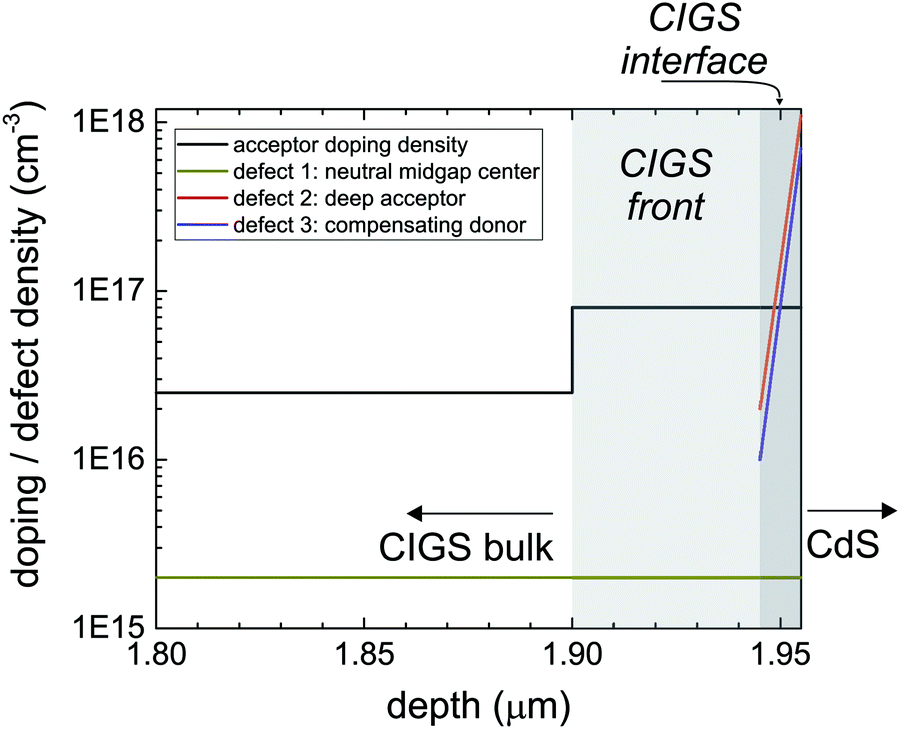 | ||
| Fig. 3 Doping and defect density profiles near the CIGS/CdS interface. Details of the defect levels can be found in Table 1. | ||
Fig. 4 shows simulated capacitance–frequency curves under different bias voltages at a temperature of 220 K, i.e. a temperature where the capacitance transition is observed experimentally (see Fig. 2). The behavior of an additional capacitance step, which is only observed in forward bias, is well reproduced by the model. Note that only the occurrence of the additional capacitance step in forward bias is simulated and not the low temperature capacitance step, which was assigned to a barrier (see Section 4).
 | ||
| Fig. 4 Simulated capacitance–frequency curves for different applied dc bias voltages at 220 K for the model summarized in Table 1. The additional capacitance step is observed when going into forward bias due to the fact that the near interface deep acceptor state crosses the Fermi level and hence can contribute to the capacitance. | ||
In order to allow a high capacitance contribution to the defect state the density was set as high as 1.1 × 1018 cm−3 directly at the interface to the CdS buffer layer. As a consequence, additional positive charge needed to be added at the interface or in the interface layer to compensate for the negative charge. This compensation is achieved by adding a single donor in the CIGS interface layer (defect 3 in Table 1). The energetic position is 0.01 eV below the conduction band to ensure a positive charge of that compensating donor. To match the smooth occurrence of the capacitance step when going into forward bias, the density of the near interface defect states (defect 2 and defect 3) is linearly graded within the 10 nm CIGS interface layer. It needs to be noted that the voltage dependent C(f) curves could also be reproduced using a homogeneous CIGS interface layer. However, the agreement of simulated and experimental data including the doping profiles determined from C(V) curves (see Section 4.3) is better using a graded CIGS interface layer.
Another important feature, which can be observed from the experimental C(f) curves (Fig. 2), is the strong increase of the capacitance plateau between the forward bias capacitance step and the capacitance due to the barrier. This plateau represents the SCR capacitance of the absorber and is roughly 45 nF cm−2 for 0 V and around 125 nF cm−2 for +0.6 V bias voltage. Such an increase could not be described by our model with a homogeneously distributed doping density of 2.5 × 1016 cm−3. The origin could be a non-homogeneously distributed doping density, i.e. a higher doping density towards the front surface of the absorber layer. This effect is captured to a certain extent also by the simulation shown in Fig. 4, where the doping densities of the CIGS front and the CIGS interface layer were set to 8 × 1016 cm−3.
For the simulations presented in Fig. 4 an acceptor level above the valence band was assumed to cause the additional forward bias capacitance step (see defect 2 in Table 1). In principle also a donor located below the conduction band could be imagined in the surface layer. However, as the inversion is generally assumed to be rather good in the absorber, the Fermi level would cross a defect state with a distance of 0.27 eV from the conduction band already at zero bias. Even for an inversion, which is less pronounced, the electrons are still majority carriers and the Fermi level would move only little with respect to voltage. As a consequence we were not able to model the voltage dependence on capacitance with a deep donor below the conduction band. In particular the capacitance step is less pronounced with a deep donor compared to the capacitance step shown in Fig. 4, which was simulated with a deep acceptor.
Alternatively the donor-like defect state could be located only in the bulk of the absorber except the interface layer. Still, for a thin (0.01 μm) surface layer the same arguments hold as above, since the absorber layer is generally still reasonably inverted at 0.01 μm from the hetero interface. For thicker interface layers (above 0.1 μm) the doping of the absorber needs to be considerably reduced (below the values obtained from C(V) measurements) in order to allow for a sufficient band bending in the absorber even at 0.6 V forward bias so that the defect state could cross the electron Fermi level.
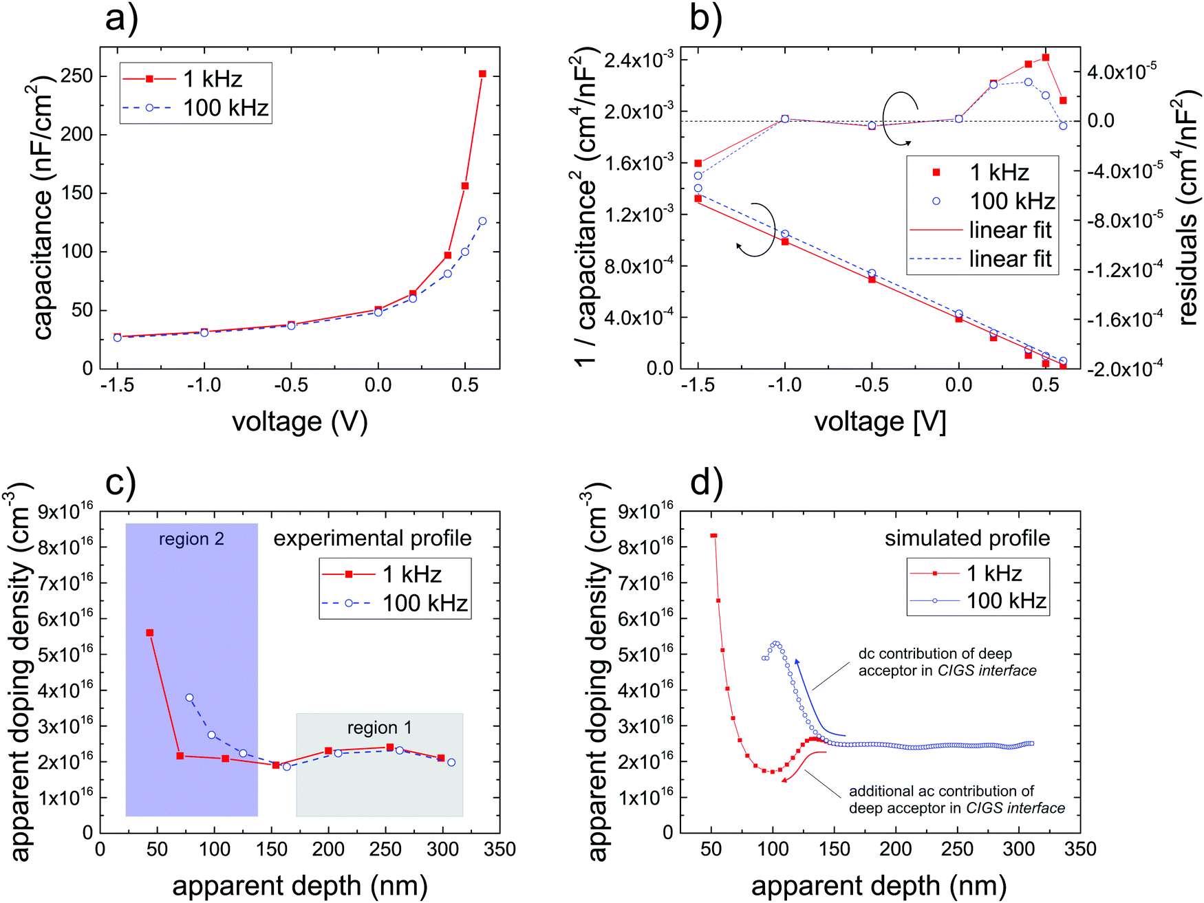
4.3 Capacitance voltage characteristics
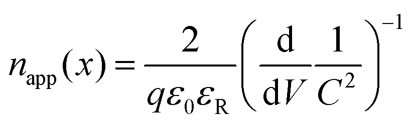
In the next step we will discuss the C(V) characteristics of the investigated device and how a near interface defect state might impact the resulting apparent doping density. The model proposed in Table 1 will be used for that purpose (see also Fig. 3).Experimentally, we have recorded admittance spectra from −1.5 V to +0.6 V. These spectra can be used to extract a C(V) curve at a certain temperature and frequency. We have chosen a temperature of 213 K (thick line in Fig. 2). Two frequencies were considered for the analysis: 1 kHz (‘low frequency’, black dot in Fig. 2) and 100 kHz (‘high frequency’, blue dot in Fig. 2). In the high frequency case the capacitance value roughly corresponds to the value directly above the low temperature capacitance step (assigned to a barrier) for all voltages. The frequency is high enough such that the near interface deep acceptor state does not respond to the ac modulation. In contrast, at low frequency, the near interface deep acceptor does respond to the ac modulation and gives an additional capacitance contribution. The extracted capacitance values with respect to voltage are plotted in Fig. 5a. From these capacitance data the Mott–Schottky plot has been calculated, which is shown in Fig. 5b. The most linear part between −1.0 V and 0.0 V has been fitted with a straight line and the residuals are plotted on the right ordinate. In forward bias an increased deviation from the straight line is observed for the low frequency case due to the additional ac contribution from the near interface deep acceptor state. From the Mott–Schottky plot the apparent doping density can be calculated using20
 | (3) |
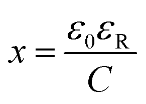 , which is called herein the apparent depth. The apparent doping profile is depicted in Fig. 5c. In this graph two different regions can be identified as marked by the grey and blue boxes. The first region corresponds to deeper probing depths (170–300 nm) measured under reverse bias conditions. The apparent doping in this region is attributed to a bulk doping density. When going into forward bias (smaller probing depths < 150 nm) the apparent doping density starts to increase (region 2). For the high frequency case this is only due to the change in the charge state of the near interface acceptor state from negatively charged to neutral. In contrast the apparent doping profile in the low frequency case is additionally influenced by the ac contribution.
 | ||
| Fig. 5 Extracted capacitance voltage data from voltage dependent admittance spectra at 213 K (a) and the calculated Mott–Schottky plot (b). The deduced apparent doping density is shown in (c). The apparent doping density calculated from simulated capacitance voltage curves at a temperature of 220 K is shown in (d) using the model summarized in Table 1. | ||
This ac contribution will show up as a decreased apparent doping density, which can slightly be identified between 75 nm and 150 nm. Another effect of the ac contribution is the decreased apparent depth due to an increased capacitance value.
In order to verify the interpretation of the experimental apparent doping profiles, the SCAPS model presented in Table 1 has been used to simulate CV curves, which already reproduced the frequency dependence of the capacitance (see Fig. 4). The simulations were carried out at a temperature of 220 K (as for the capacitance frequency curves shown in Fig. 4) and from +0.6 V to −1.5 V bias voltage at frequencies of 1 kHz and 100 kHz, i.e. the low and high frequency cases, respectively. The simulated CV curves are used to calculate the apparent doping profiles, which are shown in Fig. 5d. Under reverse bias conditions (200 nm to 300 nm) the doping density of the absorber layer is obtained. Under forward bias conditions similar trends are observed as shown experimentally (Fig. 5c). For 100 kHz (no ac contribution) and forward bias (apparent depth < 150 nm) the increase of the apparent doping density is due to the change of the occupation probability of the near interface defect state. Under these forward bias conditions the near interface deep acceptor state starts to cross the Fermi level and gets depopulated of electrons. For 1 kHz the ac contribution results in an additional decrease of the apparent doping density and the simultaneous decrease of the apparent depth. It needs to be noted that the experimental decrease of the apparent doping profile is much less pronounced. The origin could be caused by an increased doping towards the front, which deviates in shape and/or magnitude as assumed for the simulations (compare Fig. 3).
We observed good qualitative agreement of the measured and simulated apparent doping profiles. Additionally the SCAPS model describes the frequency dependence of the capacitance under various bias voltages, which supports the assumption of a near interface deep acceptor state. We note that negative charge at the interface should be avoided for the design of a CIGS solar cell.19 First, it reduces the inversion at the interface and thus could enhance interface recombination. Second, the SCR width in the absorber is reduced, which might harm the collection of photogenerated carriers. However, currently it is not possible to link the occurrence of the deep acceptor to process parameters as the deep acceptor was observed for devices with different GGI values at the front CIGS/CdS interface as well as for different RbF PDT treatments (see the ESI,† Fig S4).
In the next step we can compare the simulated apparent doping profiles (Fig. 5d) to doping profiles reported in the literature and the respective proposed models.15,25,35–37 In particular, the doping profile for the low frequency case is observed commonly and has been discussed by several authors. Kimerling has derived an analytical description of the apparent doping profile from C(V) data including a deep defect state.15 This model is often used to describe the doping profiles having a higher density far away from the junction and a smaller density close to the junction.25,35,36 The principle is that in forward bias the deep defect state does not cross the Fermi level anymore and the true doping density of the absorber is measured. The strong increase of the doping profile at small values of the apparent depth was investigated by Igalson et al.37 and attributed to a barrier at the front contact. In this model the barrier represents the minimal distance of charge modulation. However, the obtained values were always a bit off from the experimental thicknesses of the buffer, which was attributed to a barrier at the front. Here we propose a different model, which is a near interface acceptor state as experimentally measured by voltage dependent admittance spectroscopy. Unfortunately, forward bias admittance spectra are not reported in the literature and therefore no information of the near surface region could be obtained for those samples.
5. Conclusion
We have shown that the near interface CIGS absorber region can be probed by admittance spectroscopy by applying an additional bias voltage in complete solar cell devices. For the CIGS based solar cells presented here an additional capacitance step is observed in forward bias compatible with a model including an acceptor state 0.27 eV above the valence band and present only in the near surface region.The assignment of the near interface deep acceptor state was corroborated by SCAPS simulations. A model was presented, which explains the frequency and voltage dependence of the capacitance.
In the case of interface recombination, negative charge is detrimental for the solar cell performance as it reduces the inversion towards the buffer layer.19 Consequently, it is of interest to probe these defects to find process parameters to suppress the formation of these defect states.
Additionally, the presented model is applied to gain further insights into the voltage dependence of the capacitance, which is used to determine the apparent doping density of the absorber. We have shown that the profile of the apparent doping density is explained by the SCAPS model including the near interface acceptor state. Features of the apparent doping density include a small dip for small forward bias voltages and a strong increase for higher forward bias voltages.
Conflicts of interest
There are no conflicts to declare.Acknowledgements
Funding from the Swiss Federal Office of Energy (SFOE contact SI/501145-01), Swiss National Science Foundation (SNSF contract 200021_149453/1), and Swiss State Secretariat for Education, Research and Innovation (SBFI contract REF-1131-52107). The work has received support from the European Union's Horizon 2020 research and innovation program under grant agreement no. 641004 (Sharc25).References
- P. Jackson, et al., Effects of heavy alkali elements in Cu(In,Ga)Se2 solar cells with efficiencies up to 22.6%, Phys. Status Solidi RRL, 2016, 583–586 CrossRef CAS.
- I. Repins, et al., 19.9%-efficient ZnO/CdS/CuInGaSe2 solar cell with 81.2% fill factor, Prog. Photovoltaics, 2008, 16(3), 235–239 CAS.
- M. A. Contreras, et al., Optimization of CBD CdS process in high-efficiency Cu(In,Ga)Se2-based solar cells, Thin Solid Films, 2002, 403–404, 204–211 CrossRef CAS.
- A. Chirilă, et al., Potassium-induced surface modification of Cu(In,Ga)Se2 thin films for high-efficiency solar cells, Nat. Mater., 2013, 12, 1107–1111 CrossRef PubMed.
- K. Ramanathan, et al., Advances in the CIS research at NREL, Conference Record of the IEEE Photovoltaic Specialists Conference, 1997.
- K. Ramanathan, et al., Properties of Cd and Zn partial electrolyte treated CIGS solar cells, Conference Record of the IEEE Photovoltaic Specialists Conference, 2002.
- P. K. Johnson, et al., Interface properties of CIGS(S)/buffer layers formed by the Cd-partial electrolyte process, Conference Record of the IEEE Photovoltaic Specialists Conference, 2002.
- O. Cojocaru-Miŕdin, et al., Atomic-scale characterization of the CdS/CuInSe2 interface in thin-film solar cells, Appl. Phys. Lett., 2011, 98(10), 103504 CrossRef.
- O. Cojocaru-Mirédin, et al., Exploring the p-n junction region in Cu(In,Ga)Se2 thin-film solar cells at the nanometer-scale, Appl. Phys. Lett., 2012, 101(18), 181603 CrossRef.
- X. He, et al., Cd doping at PVD-CdS/CuInGaSe2 heterojunctions, Sol. Energy Mater. Sol. Cells, 2017, 164, 128–134 CrossRef CAS.
- T. Walter, et al., Determination of defect distributions from admittance measurements and application to Cu(In,Ga)Se2 based heterojunctions, J. Appl. Phys., 1996, 80(8), 4411–4420 CrossRef CAS.
- M. Burgelman, P. Nollet and S. Degrave, Modelling polycrystalline semiconductor solar cells, Thin Solid Films, 2000, 361, 527–532 CrossRef.
- R. Scheer, Activation energy of heterojunction diode currents in the limit of interface recombination, J. Appl. Phys., 2009, 105, 104505 CrossRef.
- K. Decock, et al., Defect distributions in thin film solar cells deduced from admittance measurements under different bias voltages, J. Appl. Phys., 2011, 110(6), 063722 CrossRef.
- L. C. Kimerling, Influence of deep traps on the measurement of free-carrier distributions in semiconductors by junction capacitance techniques, J. Appl. Phys., 1974, 45(4), 1839–1845 CrossRef CAS.
- M. Burgelman, et al., Advanced electrical simulation of thin film solar cells, Thin Solid Films, 2013, 535(1), 296–301 CrossRef CAS.
- K. Decock, P. Zabierowski and M. Burgelman, Modeling metastabilities in chalcopyrite-based thin film solar cells, J. Appl. Phys., 2012, 111(4), 043703 CrossRef.
- S. Lany and A. Zunger, Light- and bias-induced metastabilities in Cu(In,Ga)Se2 based solar cells caused by the (VSe-VCu) vacancy complex, J. Appl. Phys., 2006, 100(11), 113725 CrossRef.
- R. Scheer and H. W. Schock, Chalcogenide Photovoltaics: Physics, Technologies, and Thin Film Devices, Chalcogenide Photovoltaics: Physics, Technologies, and Thin Film Devices, 2011 Search PubMed.
- S. Sze and K. K. Ng, Physics of Semiconductor Devices, 3rd edn, 2006, pp. 100–102 Search PubMed.
- S. Nishiwaki, et al., Precise Se-flux control and its effect on Cu(In,Ga)Se2 absorber layer deposited at low substrate temperature by multi stage co-evaporation, Thin Solid Films, 2016, 633, 18–22 CrossRef.
- P. Reinhard, et al., Cu(In,Ga)Se2 Thin-Film Solar Cells and Modules – A Boost in Efficiency Due to Potassium, IEEE J. Photovolt., 2015, 656–663 CrossRef.
- A. R. Burgers, et al., Improved treatment of the strongly varying slope in fitting solar cell I–V curves, Conference Record of the IEEE Photovoltaic Specialists Conference, 1996.
- R. Herberholz, M. Igalson and H. W. Schock, Distinction between bulk and interface states in CuInSe2/CdS/ZnO by space charge spectroscopy, J. Appl. Phys., 1998, 83, 318–325 CrossRef CAS.
- T. Eisenbarth, et al., Interpretation of admittance, capacitance-voltage, and current-voltage signatures in Cu(In,Ga)Se2 thin film solar cells, J. Appl. Phys., 2010, 034509 CrossRef.
- F. Pianezzi, et al., Unveiling the effects of post-deposition treatment with different alkaline elements on the electronic properties of CIGS thin film solar cells, Phys. Chem. Chem. Phys., 2014, 8843–8851 RSC.
- J. T. Heath, J. D. Cohen and W. N. Shafarman, Bulk and metastable defects in CuIn1-xGaxSe2 thin films using drive-level capacitance profiling, J. Appl. Phys., 2004, 95(3), 1000–1010 CrossRef CAS.
- F. Werner, et al., Alkalie treatment of Cu(In,Ga)Se2 thin film absorbers: transport barriers and their influence on the admittance spectrum, unpublished, 2017.
- T. P. Weiss, et al., Injection current barrier formation for RbF post deposition treated Cu(In,Ga)Se2 based solar cells, to be published, 2017.
- A. Niemegeers, et al., Model for electronic transport in Cu(In,Ga) Se2 solar cells, Prog. Photovoltaics, 1998, 6(6), 407–421 CAS.
- T. P. Weiss, et al., Direct Evaluation of Defect Distributions From Admittance Spectroscopy, IEEE J. Photovolt., 2014, 4(6), 1665–1670 CrossRef.
- J. Bailey, G. Zapalac and D. Poplavskyy, Metastable defect measurement from capacitance–voltage and admittance measurements in Cu(In,Ga)Se2Solar Cells, Conference Record of the IEEE Photovoltaic Specialists Conference, 2016.
- M. Maciaszek, P. Zabierowski and K. Decock, Modeling of the impact of Se-vacancies on the electrical properties of Cu(In,Ga)Se2 films and junctions, Thin Solid Films, 2013, 535(1), 371–375 CrossRef CAS.
- M. Igalson, et al., Understanding defect-related issues limiting efficiency of CIGS solar cells, Sol. Energy Mater. Sol. Cells, 2009, 93(8), 1290–1295 CrossRef CAS.
- M. Cwil, et al., Charge and doping distributions by capacitance profiling in Cu(In,Ga)Se2 solar cells, J. Appl. Phys., 2008, 103(6), 063701 CrossRef.
- J. Heath and P. Zabierowski, Capacitance Spectroscopy of Thin-Film Solar Cells, Advanced Characterization Techniques for Thin Film Solar Cells, 2nd edn, 2016, pp. 93–119 Search PubMed.
- M. Igalson, et al., Barriers for current transport in CIGS structures, Conference Record of the IEEE Photovoltaic Specialists Conference, 2011.
Footnote |
| † Electronic supplementary information (ESI) available. See DOI: 10.1039/c7cp05236g |
| This journal is © the Owner Societies 2017 |