3D porous ZnO–SnS p–n heterojunction for visible light driven photocatalysis†
Received
16th March 2017
, Accepted 5th June 2017
First published on 5th June 2017
Abstract
A novel two-step solution approach is put forward to design a unique three dimensional (3D) porous ZnO–SnS p–n heterojunction under mild conditions. This special 3D structure is induced via flower-like ZnO in which SnS serves as an efficient photosensitizer to improve the light harvesting across the whole visible range. A profound investigation of the mechanism shows that this 3D porous ZnO–SnS material effectively integrates the large surface area and high redox potential of ZnO, and wide visible-light harvesting of SnS, which largely promotes the transfer and separation rate of carriers. The systematic study on the active species generated during the photocatalysis illustrates that it is the photoelectrons, ˙OH and O2˙− that play the crucial role in the degradation of dyes. As a result, the noble-metal free photocatalyst degrades nearly 100% of rhodamine B (RhB) within 80 min and methylene blue (MB) in 40 min under visible light. The photocatalytic activity is 10 times higher than that of the pure flower-like ZnO and two times higher than that of the SnS material. Moreover, the photocatalyst is easily separated and reused at least four times without obvious change in efficiency and properties. This work provides an effective strategy for the synthesis of 3D porous p–n heterojunction semiconductor-based photocatalysts with low cost and low toxicity, which present promising applications in the field of solar energy storage and conversion.
1. Introduction
In recent years, industrial organic dye wastewater has posed serious threats to sustainable environment development and human health. Fortunately, these thorny problems can be solved by the photocatalytic technique,1–3 which makes use of sunlight or ultraviolet light irradiation to achieve complete degradation of organic dyes in wastewater without leaving any toxic residues.4–6 Among various photocatalysts, n-type ZnO as a wide band gap semiconductor has been widely investigated7,8 because of its advantages such as low cost, abundance, relatively high efficiency and environmental friendliness.9–12 However, several formidable challenges still remain such as its narrow absorption,13 high carrier recombination rate and the intrinsic defect of photocorrosion,14 which have severely restricted its photocatalytic activity and photostability. To address these issues, an alternative strategy is to fabricate a p–n heterojunction between ZnO and a p-type material with a narrower band gap that acts as a sensitizer to absorb visible light.15–22 The heterojunction between p-type and n-type semiconductors results in the formation of a depletion layer at the p–n interfacial region, which induces an electric field and improves the separation ability of electron–hole pairs.23 Therefore, the absorption of visible light and the carrier separation capability will be enhanced at the same time. For example, Sunita and co-workers have extended the light-harvesting range and suppressed the carrier recombination of ZnO nanorods with Ag2S as a sensitizer.24 Among numerous candidates, a p-type transition metal sulfide, tin sulfide (SnS), has received considerable interest because of its good photoresponse ability. It has a narrow band gap of 1.1–1.5 eV and completed absorption of visible light during the photodegradation.25 Moreover, its excellent properties of low-toxicity, earth abundance, and high chemical stability have attracted much attention.26,27 Therefore, the combination of ZnO and SnS will be an effective strategy to obtain a novel kind of photocatalyst by integrating their advantages.
However, the current study of ZnO–SnS is mainly limited to the field of solar cells,28–34 such as the n-ZnO/p-SnS core–shell nanowire array prepared as an active layer by Zhu et al. Apart from the report on the degradation of ciprofloxacin with the ZnO–SnS heterojunction by Makama etc. in 2015,35 there are few reports on the application of ZnO–SnS in photocatalysis to date, especially a systematic study on the degradation activity and mechanism of organic dyes with high efficiency under visible light.
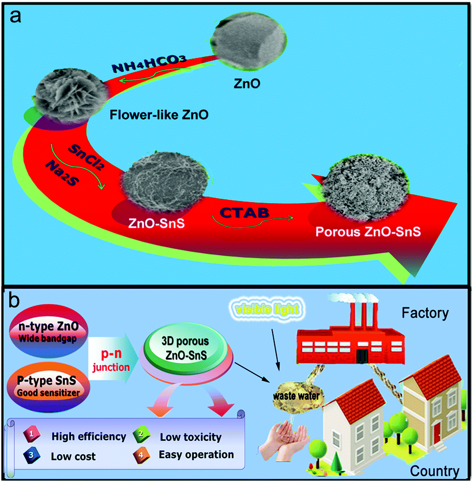
In addition, the photocatalytic activity is related to the morphology and dimensions of the material. It is known that a three-dimensional (3D) porous structure usually presents higher photocatalyst activity than a one-dimensional (1D) catalyst, because of its larger specific surface area, more excellent organic dye adsorption ability and higher utilization of the incident light.36–38 Herein, a 3D porous ZnO–SnS heterojunction was synthesized following a simple two-step solution strategy, which enjoys the advantages of high efficiency, low toxicity, low cost and easy operation. The design concept is presented in Scheme 1. Firstly, the flower-like ZnO is prepared as the foundation of the porous structure of ZnO–SnS due to its large surface area that significantly facilitates the interaction between ZnO and SnS. Afterwards, citric acid is employed as the surface-modifying ligand, which not only activates the surface of ZnO, but also facilitates the particle dispersion of the catalyst. Finally, with the addition of SnCl2·2H2O, Na2S·9H2O and CTAB surfactant, a 3D porous ZnO–SnS heterojunction is formed. This unique structure takes full advantage of the high surface area and wide light-harvesting range of ZnO and SnS, and hence effectively improves the carrier separation rate. Consequently, the 3D porous ZnO–SnS heterojunction achieves 10 times higher photocatalytic activity compared with flower like ZnO, which degrades almost 100% of RhB in 80 min under visible light with a first-order rate constant of 0.05 min−1. Moreover, after each photocatalysis reaction, the photocatalyst is easily separated and reused at least four times without any obvious change in efficiency and properties.
 |
| | Scheme 1 Schematic illustration of the 3D porous ZnO–SnS heterojunction prepared with a two-step solution method: (a) preparation process and (b) design concept of the 3D porous ZnO–SnS heterojunction. | |
2. Experimental
2.1 Materials
All of the reagents used in the experiment were analytically pure and used as received. Ammonium bicarbonate (NH4HCO3), silver nitrate (AgNO3) and zinc oxide (ZnO >99.5%) were purchased from Huadong Reagent Factory in Tianjin. Citric acid (C6H8O7) and ammonium oxalate ((NH4)2C2O4) were purchased from Beijing Chemical Factory, sodium sulfide nonahydrate (Na2S·9H2O >98%), hexadecyltrimethy ammonium bromide (CTAB) and stannous chloride (SnCl2·2H2O) were from Xilong Chemical Co., Ltd. rhodamine B (RhB), methyl orange (MO) methylene blue (MB), benzoquinone (BQ) and tert-butanol (t-BuOH) were from Guangdong Chemical Factory.
2.2 Synthesis of 3D flower-like ZnO superstructures
In order to increase the surface area of the sample, analytically pure zinc oxide was used to prepare flower-like ZnO. In a typical procedure, 2 g NH4HCO3 was dissolved in 150 mL purified water. Afterwards, 4 g zinc oxide was added into the above solution, stirring at 40 °C for 20–30 min, and then, the obtained sample was washed and centrifuged with deionized water several times. Finally, the product was dried at 60 °C for further application.
2.3 Synthesis of the SnS material
In a typical procedure, 158 mg SnCl2·2H2O and 36.5 mg C6H8O7 were dissolved in 100 mL water. After stirring for 1 h, 25 mL Na2S·9H2O (0.025 M) was added dropwise into the above solution. After continuously stirring for another 1 h, a brown SnS material was finally obtained, washed with deionized water several times and dried at 60 °C for future characterization.
2.4 Synthesis of a 3D ZnO–SnS porous heterojunction
The synthesis procedure of the ZnO–SnS heterojunction with the optimal ratio of Zn2+ to Sn2+ equal to 4 (Table S1, ESI†) was as follows: 56 mg flower-like ZnO and 36.5 mg C6H8O7 were mixed together in a round flask and dispersed well in water under continuous stirring. Afterwards, the mixture was heated up to 40 °C for 2 h. Then, 40 mg SnCl2·2H2O and 10 mg CTAB were gradually dissolved in 25 mL water and added dropwise into the above solution. After constantly stirring for another 2 h, 38 mg Na2S·9H2O was dispersed in 25 mL water and added dropwise into the stannous chloride solution with a dropping funnel. After stirring for 1 h, the solution gradually turned light-yellow, indicating the formation of a ZnO–SnS heterojunction. By contrast, the experiment was conducted without the addition of CTAB. Finally, the obtained products were separated and collected after being washed with deionized water several times. It should be noted that this dropwise addition of SnCl2·2H2O and Na2S·9H2O was very important to slow down the ion-exchange reaction between [Zn2+O2−] ions and [Sn2+S2−] ions on the surface of ZnO.39
2.5 Characterization
Powder X-ray diffraction patterns (XRD) were acquired by a Shimadzu XRD-6000 diffraction system with high-intensity Cu Kα radiation. Field-emission scanning electron microscope (FESEM) images were obtained on a Hitachi S-4800 operated at the voltage of 5.0 kV. Transmission electron microscopy (TEM) images were acquired on a JEOL 2010 at an accelerating voltage of 200 kV. X-ray photoelectron spectrometry (XPS) was carried out with a VG ESCALAB MKII spectrometer to study the valence states of the existing elements. UV-vis absorption spectra were obtained using a Shimadzu 3600 UV-visible-NIR spectrophotometer. Photoluminescence (PL) measurements were achieved with a RF-5301PC instrument. The electrochemical impedance spectra (EIS) measurements were conducted by using a CHI 660E electrochemical workstation, with three electrodes including a saturated calomel electrode, a Pt sheet and the as prepared steel net corresponding to the reference electrode, counter electrode and working electrode respectively. 1 M Na2SO4 was used as the electrolyte. The preparation of the working electrode was as follows: firstly, a mixture of the active substance, acetylene black and polyvinylidene fluoride (PVDF) with the mass ratio of 8![[thin space (1/6-em)]](https://www.rsc.org/images/entities/char_2009.gif) :1:1 was ground evenly; then, 1–2 drops of N-methyl pyrrolidone (NMP) were added to the mixture to form a homogeneous slurry; and finally, a certain amount of the slurry was smeared onto the steel net, and dried at 60 °C for 12 h. The cyclic voltammogram(CV) test was conducted in the same three-electrode cell system as the EIS measurements with a scan rate of 10 mV s−1 and a voltage window of −0.5–0 V. Nitrogen adsorption–desorption (BET) was examined using a micrometric ASAP 2020 instrument, with the degassing temperature of 200 °C. The Fourier transform infrared (FT-IR) spectrum was taken on a Nicolet AVATAR 360 FT-IR spectrophotometer.
:1:1 was ground evenly; then, 1–2 drops of N-methyl pyrrolidone (NMP) were added to the mixture to form a homogeneous slurry; and finally, a certain amount of the slurry was smeared onto the steel net, and dried at 60 °C for 12 h. The cyclic voltammogram(CV) test was conducted in the same three-electrode cell system as the EIS measurements with a scan rate of 10 mV s−1 and a voltage window of −0.5–0 V. Nitrogen adsorption–desorption (BET) was examined using a micrometric ASAP 2020 instrument, with the degassing temperature of 200 °C. The Fourier transform infrared (FT-IR) spectrum was taken on a Nicolet AVATAR 360 FT-IR spectrophotometer.
3. Results and discussion
3.1 Morphology and structure of the 3D porous ZnO–SnS heterojunction
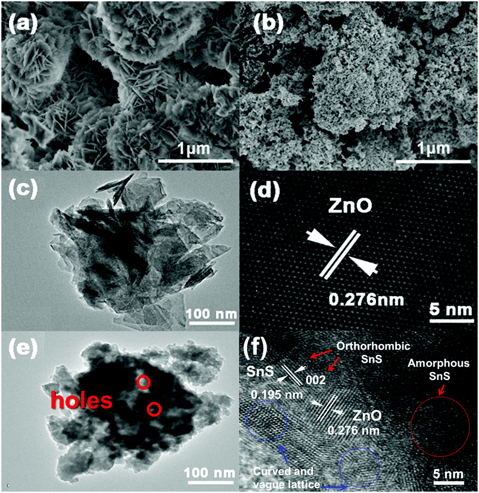
As illustrated in the SEM picture (Fig. 1a), ZnO treated with NH4HCO3 exhibits a 3D flower-like morphology with an average diameter of 0.5–1 μm. When SnS and CTAB are introduced, the obtained ZnO–SnS heterojunction gives a relatively fluffy 3D porous microstructure with a rough surface (Fig. 1b). Meanwhile, the TEM image (Fig. 1c) also exhibits a flower-like structure of ZnO. The fringe with d of 0.276 nm in the HRTEM image matches well with the (002) crystallographic plane of ZnO (Fig. 1d). After introducing SnS and CTAB, the composite exhibits a 3D structure with many small holes (Fig. 1e), which is consistent with the SEM result. This structure will possess high photocatalytic activity with broader light harvesting ability and more reactive sites. Moreover, the HRTEM image of the composite shows both the (002) crystallographic plane of ZnO and the (002) crystallographic plane of SnS with the lattice space of d = 0.195 nm (Fig. 1f), demonstrating the successful preparation of the ZnO–SnS heterojuction. It should be noted that owing to the weak crystallinity of SnS, amorphous SnS can also be observed as a random layer lattice denoted by the red circle. Furthermore, the lattice of ZnO–SnS seems vague and curved, which may result from the existence of Sn2+ defects, oxygen deficiency and/or oxygen vacancy defect complexes in the heterojunction.40
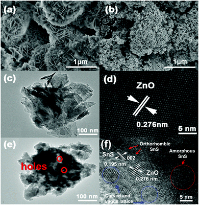 |
| | Fig. 1 SEM images of (a) flower-like ZnO and (b) the 3D porous ZnO–SnS heterojunction (molar ratio of Zn2+:Sn2+ = 4:1), (c) TEM and (d) HRTEM images of flower-like ZnO, and (e) TEM and (f) HRTEM images of the 3D porous ZnO–SnS heterojunction. | |
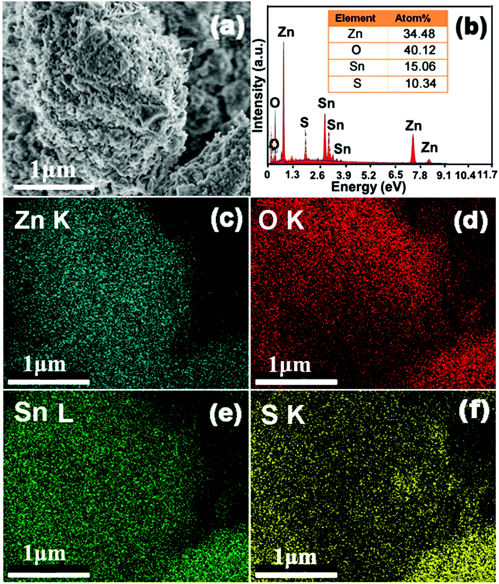
Elemental mapping was conducted to decipher the composition and elemental distribution of the ZnO–SnS heterojunction (Fig. 2). Meanwhile, the blue, red and yellow color images are distinctly acquired at the K-line spectra of Zn, O and S elements, respectively, while the green color of the image corresponds to the L-line spectra of Sn, showing the coexistence of Zn, O, Sn and S elements in the ZnO–SnS heterojunction. The corresponding atom contents in Fig. 2b are 34.48%, 40.12%, 15.06% and 10.34% for Zn, O, Sn and S, respectively. It is observed that the contents of Sn and O are a little higher than those of S and Zn, which may be due to the formation of a small amount of SnO and O2 from the atmosphere. However, it has little effect on the catalyst activity.41
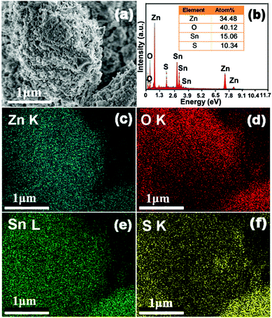 |
| | Fig. 2 Mapping and EDX pictures of the 3D porous ZnO–SnS heterojunction, indicating the coexistence and homogenous distribution of Zn, O, Sn and S elements in the ZnO–SnS heterojunction. | |
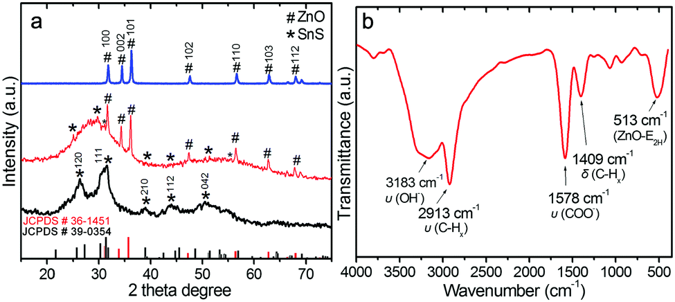
XRD measurements of ZnO, SnS and ZnO–SnS were carried out to investigate their crystallinity and phase composition (Fig. 3a). Meanwhile, all the diffraction peaks of the blue line are well consistent with the wurtzite phase of ZnO (JCPDS: 36-1451),42 which contains nine main sharp and intensive peaks from 30 to 70°, ascribed to its high purity and crystallinity. Besides, the wide diffraction peaks at 26.9° and 31.5°of the black line are attributed to the (120) and (111) planes, which agrees well with the orthorhombic phase of SnS (JCPDS no. 39-0354),24 while the whole shallow peak indicates the existence of amorphous SnS. SEM and TEM (low and high) images show that the size of the SnS is quite small (Fig. S1a and b, ESI†). The HRTEM image of SnS further confirms the co-existence of amorphous and orthorhombic phases in the obtained SnS. This probably results from its special preparation process. That is, the addition of citric acid and low synthesis temperature (room temperature) is unfavorable to the adequate growth of SnS, which finally brings about its poor crystallinity, irregular shape and small particle size (Fig. S1, ESI†). When it comes to the ZnO–SnS patterns (Fig. 3a, red line), sharp peaks of wurtzite phase ZnO are observed. However, apart from several weak peaks, no obvious characteristic diffraction peaks of SnS are observed owing to its low loading content and weak crystallinity. On the other hand, this also indicates the good dispersion of small SnS nanoparticles on the ZnO surface, which is consistent with the TEM result.
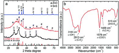 |
| | Fig. 3 (a) Powder XRD patterns of ZnO, SnS and the 3D porous ZnO–SnS heterojunction, and (b) FTIR spectra of the ZnO–SnS heterojunction, certifying the successful preparation and high purity of the as prepared ZnO–SnS photocatalyst. | |
In order to check the bond structure of ZnO–SnS, FTIR measurement was carried out (Fig. 3b). The absorption at 3183 cm−1 is attributed to the stretching mode of hydroxyl groups, while the peak observed at 1578 cm−1 is attributed to the O–H asymmetrical stretching of zinc carboxylate ions. Meanwhile, the carboxylate probably results from reactive carbon during synthesis, while the hydroxyl comes from the hygroscopic nature of ZnO.43,44 Moreover, the peaks located at 2913 and 1409 cm−1 confirm the stretching vibration and deformation vibration of the C–H mode from alkane groups,45 respectively, while the band at 513 cm−1 may be associated with oxygen deficiency and/or oxygen vacancy (VO) defect complexes in ZnO.46,47 However, it should be noted that almost all of the peak positions present a small shift toward lower binding energy compared with the related literature, which may be from the special interaction between the functional groups on the surface of the ZnO and SnS.43
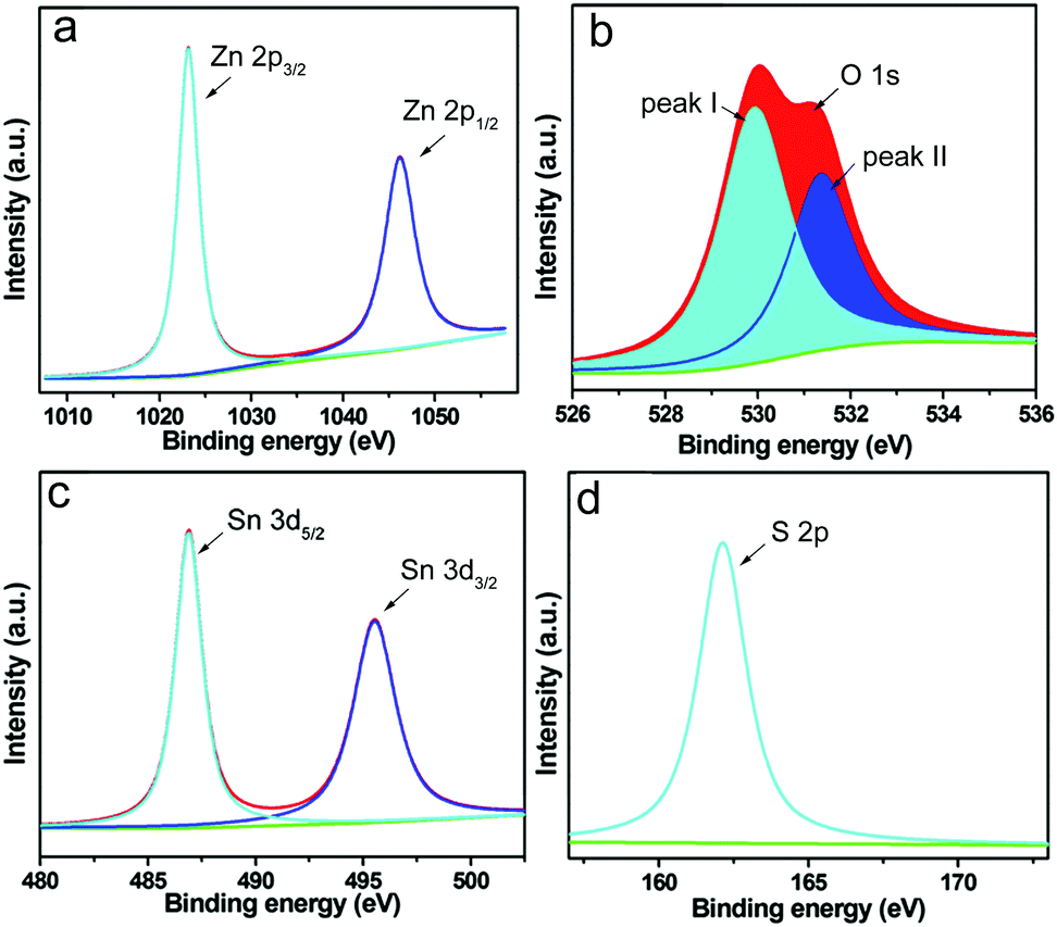
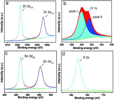
XPS was performed in order to study the valence states of the elements in the obtained sample. In Fig. 4, the peaks of Zn, O, Sn and S are clearly observed. The two strong separated contributions at 1021.8 and 1044.8 eV in the high resolution spectra of Zn are assigned to the binding energy of the Zn 2p3/2 and Zn 2p1/2 orbitals, which is in accordance with Zn(II). Moreover, the satellite line in Fig. 4b is consistent with the characteristic peak of O 1s, which is fitted to separate peaks (I and II) derived from two different kinds of O species. Meanwhile, peak I should be associated with the lattice oxygen (Ol) of ZnO,48 while peak II is from chemisorbed oxygen (Oa) rooted in the surface hydroxyl group.49 In addition, the peaks at the binding energy of 484.9 and 497.2 eV in Fig. 4c correspond to the characteristic peaks of Sn 3d5/2 and Sn 3d3/2, which are probably assigned to SnS, while the peak of S 2p observed at 163.9 eV in Fig. 4d indicates the presence of S element.
 |
| | Fig. 4 High-resolution XPS spectra of (a) Zn 2p, (b) O 1s, (c) Sn 3d and (d) S 2p in the as synthesized ZnO–SnS. | |
3.2 Photocatalytic properties
In order to evaluate the degradation activity of the photocatalyst, RhB was taken to evaluate the performance of ZnO, SnS and ZnO–SnS. Typically, 10 mg of the catalyst was dispersed into 25 mL of 10−5 M RhB aqueous solution by constant stirring and maintained in the dark for 20 min and irradiation was conducted using a 300 W Xe lamp with UV cutoff filters (λ > 420 nm) (CEL-SPH2N, Beijing). In a certain time interval (10 min), 3 mL of the reaction solution was extracted to study the RhB concentration using a UV-vis spectrophotometer. The degradation efficiency of the photocatalyst is defined as eqn (1):50| | | Degradation (%) = C/C0 × 100% | (1) |
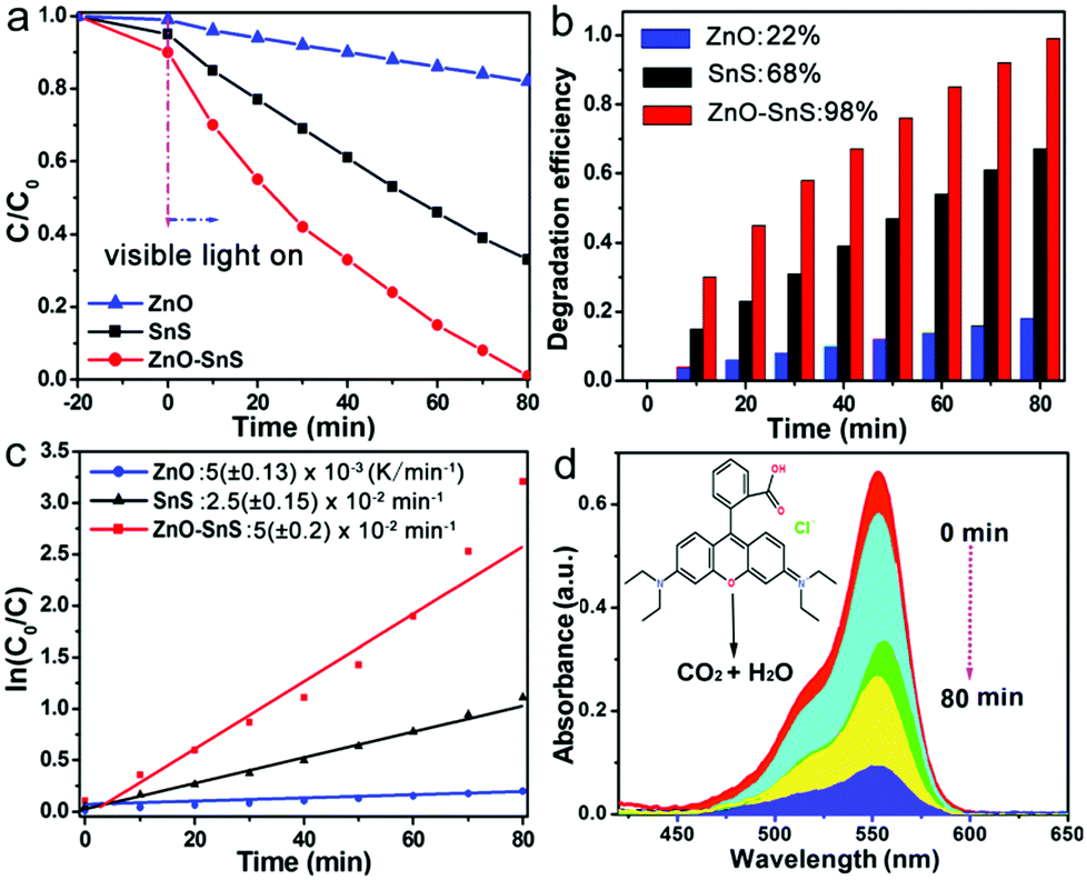
where C0 and C are the initial and remaining concentration of RhB after the reaction. The degradation rate is calculated using eqn (2): in which k is considered as the degradation rate constant. As observed from Fig. 5a, after 20 min of constant stirring in the dark, all RhB solutions containing the three photocatalysts reveal a slight decrease in absorbance, which is attributed to the adsorption effect of the dye on the surface of the photocatalysts. However, once the RhB solution is irradiated under visible light, its absorbance displays a rapid decline with SnS and ZnO–SnS as the catalyst. After 80 min of visible light irradiation, the conversion rates of RhB by SnS and flower-like ZnO are 68% and 22%, respectively, while RhB can be almost totally degraded by the ZnO–SnS heterojunction under the same conditions (Fig. 5b). Besides, according to eqn (2), the degradation rate constant of 3D porous ZnO–SnS is calculated to be about 0.05 min−1, which is 2 times higher than that of SnS and 10 times higher than that of flower-like ZnO (Fig. 5c and Table S2, ESI†). Its corresponding degradation process by the ZnO–SnS heterojunction is illustrated in Fig. 5d, from which the absorbance of RhB at 552 nm shows a significant decrease and finally vanishes in 80 min. The 3D porous ZnO–SnS has an outstanding photocatalysis character compared with other SnS based photocatalysts. A detailed comparison of performance between this work and previous reports is listed in Table S3 (ESI†).27
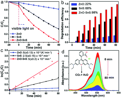 |
| | Fig. 5 (a) Photocatalytic degradation curves, (b) degradation efficiency and (c) plot of ln(C0/C) of flower-like ZnO, SnS and the 3D porous ZnO–SnS heterojunction on the photodegradation of RhB in 80 min, and (d) absorption curve of RhB solution with the 3D porous ZnO–SnS heterojunction as a catalyst under visible light (wavelength of incident light: λ > 420 nm, 10 mg photocatalyst in 25 mL of 1 × 10⁻⁵ M RhB aqueous solution, and 300 W xenon lamp as the light source). | |
In addition, to further investigate the universality of the ZnO–SnS photocatalyst, parallel experiments were carried out to degrade MO and MB with the same experiment parameter (10 mg of the catalyst was dispersed into 25 mL of 10−5 M MB or MO solution). The degradation efficiency was shown in Fig. S2 (ESI†). It is observed that MB can be completely decomposed in 40 min, while it takes MO almost four times (150 min) longer to be degraded, which may be attributed to the surface charge properties of ZnO–SnS. As seen from the FTIR spectrum, the stretching vibrations of COOH− and OH− are observed,51 which certifies the negative charge property of the ZnO–SnS surface. Besides, it is widely known that RhB and MB are cationic dyes, while MO is an anionic dye. Therefore, there will be a good electrostatic interaction between ZnO–SnS and the cationic dyes. This increases the carrier transfer rate caused by the easy adsorption of the cationic dyes on the surface of ZnO–SnS, while for anionic dyes, electrostatic repulsion between ZnO–SnS exists, and this effect is aggravated with the increase of reaction time. This view can be further proved by the different adsorption degree of RhB, MB and MO under dark conditions (Fig. 5a and Fig. S1, ESI†). Hence, ZnO–SnS has higher photocatalytic activity for cationic dyes. The better adsorption and degradation ability of MB than RhB may be attributed to the more complex structure of RhB.52
3.3 Catalytic mechanism
To further understand the reasons for the enhanced catalytic activity of ZnO–SnS, the catalytic mechanism was systematically investigated. Generally, the photocatalytic activity of a semiconductor is mainly determined by three factors: the surface area, light harvesting capacity and carrier transfer capacity of the catalyst.
3.3.1 Large surface area.
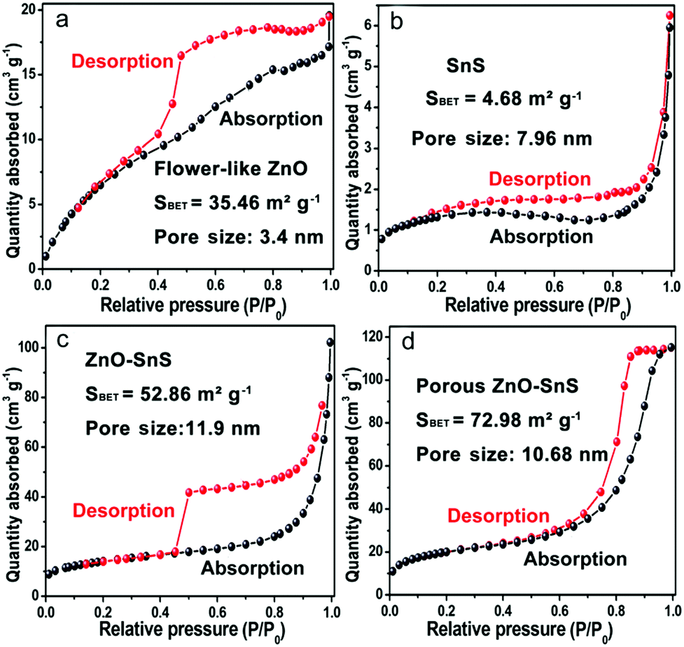
The formation of a porous 3D structure results in a high specific surface area of the catalyst, which increases the utilization of incident light and the contact between the catalyst and pigments. From the BET surface test in Fig. 6(a–d), all of the photocatalysts reveal type IV isotherms with a hysteresis loop, from which the existence of a mesopore distribution is confirmed. The BET surface area for flower-like ZnO, SnS, ZnO–SnS and 3D porous ZnO–SnS is 35.46, 4.68, 52.86 and 72.98 m2 g−1, respectively. It is worth noting that the 3D porous ZnO–SnS heterojunction exhibits a relatively higher BET surface area compared with flower-like ZnO and SnS owing to its special structure, which is of great significance to achieve an efficient photocatalysis activity. This is why ZnO–SnS exhibits higher adsorption degree of RhB than ZnO and SnS even under dark conditions.
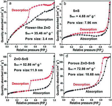 |
| | Fig. 6 Typical nitrogen adsorption and desorption isotherms of (a) ZnO, (b) SnS, (c) ZnO–SnS and (d) the 3D porous ZnO–SnS heterojunction, demonstrating the relatively high area of the 3D porous ZnO–SnS heterojunction. | |
3.3.2 Wide light-harvesting ability.
As certified in Fig. 7a, ZnO shows a narrow absorption from 300–550 nm while SnS enjoys a wide absorption range from 300 to 900 nm. Therefore, the ZnO–SnS heterojunction displays a relatively broader optical absorption capability across the entire visible light spectrum, showing it is an efficient visible light-sensitive photocatalyst. Especially, the band edge level of semiconductors is closely related to their absorbance value, which is critical for determining their degradation activity. The corresponding data are presented in Fig. 7b. In general, the potential conduction band (ECB) and valence band (EVB) edges of a semiconductor are calculated by Mulliken electronegativity theory expressed as eqn (3)–(5):53where Eg is the band gap of the semiconductor, and Ee is considered as 4.5 eV from the energy of free electrons. χ is the electronegativity of the semiconductor calculated by the geometric mean of the absolute electronegativity of the constituent elements. According to the Pearson Absolute Electronegativity,54 the absolute electronegativity of O, S, Sn and Zn is 7.54, 6.22, 4.30 and 4.45 eV, respectively. Accordingly, χZnO = (χZn·χO)1/2 = 5.79 eV while χSnS = (χSn·χS)1/2 = 5.17 eV. According to the Kubelka–Munk method,55 the relationship between the band gaps and the UV-vis spectra of semiconductors follows eqn (6):where n is determined by the electronic transition type of the semiconductor. n = 1/2 for the direct band gap semiconductor while n = 2 indicates an indirect band gap semiconductor. In the present study, n is chosen as 1/2 to obtain the direct band gap of ZnO and SnS.56α, h and ν correspond to the absorption coefficient, Planck constant and frequency of incident light, respectively; A is a proportional constant.24 Thus, the band gaps of ZnO and SnS are 3.27 and 1.50 eV. Moreover, according to the Mulliken electronegativity equations,54 the top of the VB and the bottom of the CB of ZnO are calculated to be 2.81 and −0.46 V (vs. NHE), while the VB and CB of SnS are estimated to be 1.38 and −0.12 V, respectively. Besides, the above calculated energy level position of the VB and CB of ZnO and SnS confirms the type I p–n heterojunction (Fig. 7c).
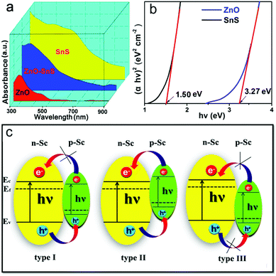 |
| | Fig. 7 (a) UV spectra of flower-like ZnO, SnS and the 3D porous ZnO–SnS heterojunction at wavelengths ranging from 300–900 nm, (b) Kubelka–Munk method: the (αhv)2 plot as a function of the photon energy to determine the band gap of the ZnO and SnS sample and (c) pictures of three types of p–n junction, illustrating the wide light harvesting range and type I p–n junction of the ZnO–SnS photocatalyst. | |
3.3.3 High carrier transfer ability.
Electrochemical impedance spectra (EIS) Nyquist plots were used to investigate the carrier separation and transfer ability of ZnO, SnS and the ZnO–SnS heterojunction, from which the heterojunction gives a smaller semicircle at high frequencies compared with ZnO and SnS (Fig. 8a). This suggests its decreased charge transfer resistance. More effective electron–hole pair separation and faster carrier transfer rate are received in the interface of the ZnO–SnS electrode.14,57,58 Besides, the cyclic voltammogram (CV) graph in Fig. 8b further certifies the enhanced carrier transfer rate of ZnO–SnS, from which the ZnO–SnS heterojunction presents obviously the highest current density, indicating that an enhanced electron transfer rate is achieved by the ZnO–SnS heterojunction.14,59,60
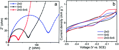 |
| | Fig. 8 (a) EIS of ZnO, SnS and the 3D porous ZnO–SnS heterojunction, indicating a faster transfer of charge carriers and higher electron–hole pair separation ability of the 3D porous ZnO–SnS heterojunction and (b) CV of ZnO, SnS and ZnO–SnS working electrodes, indicating higher carrier transfer ability of ZnO–SnS. | |
3.3.4 Role of active species.
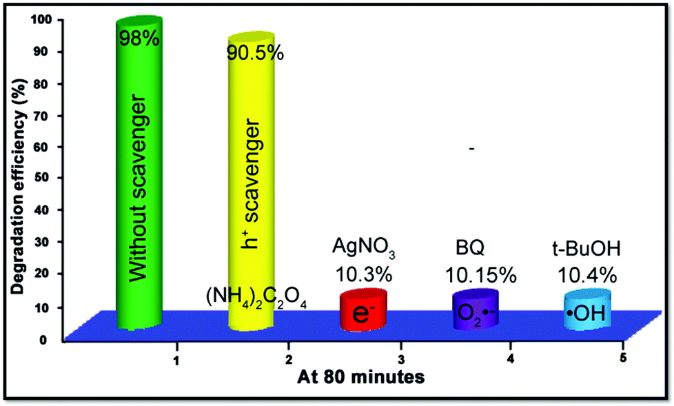
In order to study the role of active substance including electrons (e−), holes (h+), ˙OH and O2˙− during the process of catalytic reaction, 1 mmol of AgNO3, (NH4)2C2O4, t-BuOH, and benzoquinone (BQ) were added into 25 mL 10−5 M RhB solution as electron, hole, ˙OH and O2˙− sacrificial agents, respectively. The results of the trapping experiments are exhibited in Fig. 9. The degradation efficiency of RhB just reveals a slight decline from 98% to 90.5% with the existence of (NH4)2C2O4, while the addition of AgNO3, BQ and t-BuOH quenchers greatly reduced the catalytic activity to about 10%, indicating that electrons, ˙OH and O2˙− all play crucial roles in the procedure of photocatalysis.
 |
| | Fig. 9 Parallel experiments with various active species scavengers for the photodegradation of RhB by the ZnO–SnS 3D porous photocatalyst under visible light for 80 min, indicating that electrons, ˙OH and O2˙− play crucial roles in the procedure of photocatalysis. | |
A possible catalytic process is illustrated in Fig. 10 based on the above investigation. The p–n junction formed at the interface of n-ZnO and p-SnS gives rise to carrier transfer between ZnO and SnS until their Fermi levels align and reach the thermal equilibrium state. Generally, a photocatalyst with a special p–n junction is employed to reduce the recombination rate of photogenerated electrons and holes through an internal electric field, so that high photocatalytic activity is achieved. Meanwhile, the carrier separation ability is based on the matched band gap structure of the two semiconductors,18,58 which is responsible for an efficient carrier generation and separation process. However, the band positions of ZnO and SnS calculated above indicates the formation of a type I p–n heterojunction, which seems adverse to the electron transfer ability. Nevertheless, the EIS and CV results do confirm the enhanced carrier transfer rate of ZnO–SnS compared to pure ZnO and SnS, and there must be other ways to facilitate the transfer of electrons. It is confirmed by the previous research and the characterization results of TEM and FTIR spectra49 that a defect level exists in ZnO–SnS.61–63 In order to determine the type of the defect level (VO, Oietc.), the PL spectrum shows green emission at 540 nm of ZnO–SnS (Fig. S3, ESI†), confirming the defect type of VO.64–66 Because the energy level of VO is about 0.9 V deeper than that of the CB of ZnO (−0.46 V),47,67 SnS will possess a higher CB (−0.12 V) compared with VO (Fig. 10a). Therefore, the photoelectron in SnS can be easily transferred to VO of ZnO, which forms a quasi-type II p–n junction and greatly promotes the separation and transfer of carriers. The junction may partly compensate the losses induced by the initial energy barrier in the following way: when carriers diffuse on the interface of the two semiconductors, a space charge region is formed between n-type ZnO and p-type SnS (Fig. 10b). For the purpose of achieving an equilibrium condition, charge carriers diffuse and drift between SnS and ZnO, where a depletion layer is created because of the formation of the positive charge at the n-type ZnO and negative charge at the p-type SnS. This is helpful to separate the optical carriers present in the diffusion region: the excited electrons on the SnS surface will transfer to the capture center (VO) of ZnO, whereas holes on ZnO will migrate to SnS. This not only facilitates the charge separation but also accumulates electrons and holes in SnS and ZnO (eqn (7)). Considering the higher reduction capacity of ZnO (−0.46 V vs. NHE) than O2/O2˙− (−0.28 V), the gathered electrons on ZnO will absorb O2 and generate O2˙− (eqn (8)), which will then react with H2O to produce H2O2 and ˙OH (eqn (9)). H2O2 will then change into the active substance ˙OH and finally degrade the organic dye to CO2 and H2O (eqn (10) and (11)). Besides, owing to the weak oxidation potential of SnS (1.38 V vs. NHE) compared with RhB (−5.96 eV vs. vacuum,68 the value of the vacuum potential relative to NHE (ϕ) ranges from ϕ = 4.44–4.85 V from the literature),69,70 holes on the SnS surface have the possibility to convert organic dyes to intermediate colourless compounds (just like aldehyde and acid),50,71,72 and further oxidize them to CO2 and H2O (eqn (12)).
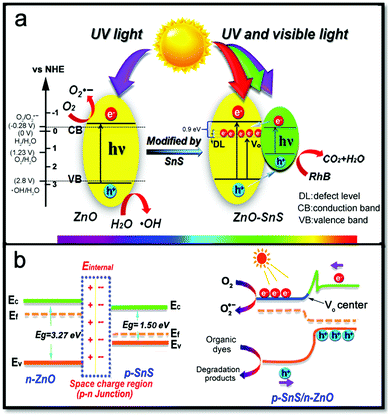 |
| | Fig. 10 Mechanism for the degradation procedure of RhB with the 3D porous ZnO–SnS heterojunction as a catalyst: (a) the design of the p–n heterojunction with enhanced light harvesting range and (b) efficient carrier separation and transfer rate of the heterojunction. | |
As a consequence, the ZnO–SnS heterojunction exhibits enhanced catalytic activity compared to pure SnS and ZnO.73,74
| | | ZnO–SnS + hν → ZnO(e−) + SnS(h+) | (7) |
| | | O2˙− + H2O → H2O2 + ˙OH | (9) |
| | | ˙OH + organic dye → CO2 + H2O | (11) |
| SnS(h+) + organic dye → intermediate colorless |
| | | compounds (aldehyde or acid) → CO2 + H2O | (12) |
4. Reusability of the catalyst
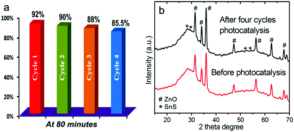
Finally, to test the stability and reusability of the ZnO–SnS heterojunction, cycling experiments were carried out in the photodegradation of RhB under visible light. After another four cycles of photodegradation, there is no significant change in the photocatalytic activity of the ZnO–SnS heterojunction (Fig. 11a). The degradation efficiency for the four cycles is found to be slightly decreased from 92% to 85.5%, which may be rooted in the photo-bleaching on the surface of ZnO–SnS.75,76 The XRD pattern (Fig. 11b) of the ZnO–SnS heterojunction after four photocatalytic reactions still reveals that the phase and structure remain intact.39 These results indicate that the ZnO–SnS heterojunction photocatalyst is sufficiently stable and not deactivated during the photodegradation of the organic dye.
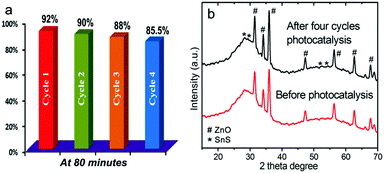 |
| | Fig. 11 (a) Recyclability test of the photocatalytic decomposition of RhB in four catalytic cycles under visible light and (b) XRD patterns of the ZnO–SnS heterojunction before and after photocatalytic reaction, indicating the high stability of 3D porous ZnO–SnS. | |
5. Conclusions
The concept of this study is to design a 3D porous ZnO–SnS p–n heterojunction photocatalyst with n-ZnO and p-type photosensitizers (SnS). Benefiting from its advantages of high surface area, wide light-harvesting ability and high carrier transfer ability, the ZnO–SnS heterojunction gives rise to an obviously enhanced photocatalytic activity in the degradation of RhB and MB under visible light irradiation, which is 10 times higher than that of flower-like ZnO with a first-order rate constant of 0.05 min−1 during the degradation of RhB. Furthermore, the catalyst possesses high stability and reusability, and can be reused for at least four consecutive runs without appreciable loss.
This work is of great significance owing to the following innovations. Firstly, it empowers us to design a novel environmentally friendly photocatalyst for handling organic dyes with a facile solution method. Secondly, it testifies the possibility of using SnS as an environmentally amicable sensitizer that may substitute Cd-based sensitizers. Thirdly, it furnishes researchers a fresh idea to explore 3D porous structures in the field of photocatalysis.
Acknowledgements
This work was supported by the NSFC (21574018 and 51433003), the Science Technology Program of Jilin Province (20130204025GX), Jilin Provincial Education Department (543), Changbai Mountain Scholar Project by Education Department of the Jilin Province, and Jilin Provincial Key Laboratory of Advanced Energy Materials (Northeast Normal University).
Notes and references
- Z. Zou, J. Ye, K. Sayama and H. Arakawa, Nature, 2001, 414, 625 CrossRef CAS PubMed.
- F. Zhai, H. T. Wei, S. M. Zhan, G. Jin, B. Yang, H. Z. Sun and Z. H. Huang, Chin. J. Polym. Sci., 2015, 33, 215 CrossRef CAS.
- X. Wang, C. Li and G. Shi, Phys. Chem. Chem. Phys., 2014, 16, 10142 RSC.
- F. Wang, S. Song, K. Li, J. Li, J. Pan, S. Yao, X. Ge, J. Feng, X. Wang and H. J. Zhang, Adv. Mater., 2016, 28, 10679 CrossRef CAS PubMed.
- Y. Li, S. Ouyang, H. Xu, X. Wang, Y. Bi, Y. Zhang and J. Ye, J. Am. Chem. Soc., 2016, 138, 13289 CrossRef CAS PubMed.
- X. Lin, Y. S. Wang, J. Zheng, C. Liu, Y. Yang and G. B. Che, Dalton Trans., 2015, 44, 19185 RSC.
- Y. M. Liang, N. Guo, L. L. Li, R. Q. Li, G. J. Ji and S. C. Gan, New J. Chem., 2016, 40, 1587 RSC.
- N. Caicedo, J. S. Thomann, R. Leturcqa and D. Lenoble, CrystEngComm, 2016, 18, 5502 RSC.
- H. Kim, D. Jeong and D. Jang, CrystEngComm, 2016, 18, 898 RSC.
- J. P. Wang, Y. M. Chen, W. H. Shen, Z. Q. Zhu, Y. S. Xu and Y. J. Fang, Catal. Commun., 2017, 89, 52 CrossRef CAS.
- Z. C. Wu, H. Wang, Y. J. Xue, B. E. Li and B. Y. Geng, J. Mater. Chem. A, 2014, 2, 17502 CAS.
- Z. L. Zhang, Y. J. Ji, J. Li, Y. X. Zhu, Z. Y. Zhong and F. B. Su, CrystEngComm, 2016, 18, 2808 RSC.
- S. A. Ansari, M. M. Khan, M. O. Ansari, J. Lee and M. H. Cho, J. Phys. Chem. C, 2013, 117, 27023 CAS.
- C. Han, Z. Chen, N. Zhang, J. C. Colmenares and Y. J. Xu, Adv. Funct. Mater., 2015, 25, 221 CrossRef CAS.
- J. Yan, L. Zhang, H. Yang, Y. Tang, Z. Lu, S. Guo, Y. Dai, Y. Han and M. Yao, Sol. Energy, 2009, 83, 1534 CrossRef CAS.
- H. Abdullah, D. H. Kuo, Y. R. Kuo, F. A. Yu and K. B. Cheng, J. Phys. Chem. C, 2016, 120, 7144 CAS.
- D. Sarkar, C. K. Ghosh, S. Mukherjee and K. K. Chattopadhyay, ACS Appl. Mater. Interfaces, 2013, 5, 331 CAS.
- H. Xu, Y. Xu, H. Li, J. Xia, J. Xiong, S. Yin, C. Huang and H. Wan, Dalton Trans., 2012, 41, 3387 RSC.
- J. S. Jang, H. G. Kim and S. H. Lee, J. Phys. Chem. Solids, 2012, 73, 1372 CrossRef.
- D. K. Ma, M. L. Guan, S. S. Liu, Y. Q. Zhang, C. W. Zhang, Y. X. He and S. M. Huang, Dalton Trans., 2012, 41, 5581 RSC.
- G. G. Liu, G. X. Zhao, W. Zhou, Y. Y. Liu, H. Pang, H. B. Zhang, D. Hao, X. G. Meng, P. Li, T. Kako and J. H. Ye, Adv. Funct. Mater., 2016, 26, 6822 CrossRef CAS.
- K. Chang, X. Hai, H. Pang, H. B. Zhang, L. Shi, G. G. Liu, H. M. Liu, G. X. Zhao, M. Li and J. H. Ye, Adv. Mater., 2016, 28, 10033 CrossRef CAS PubMed.
- A. E. Kandjani, Y. M. Sabri, S. R. Periasamy, N. Zohora, M. H. Amin, A. Nafady and S. K. Bhargava, Langmuir, 2015, 31, 10922 CrossRef CAS PubMed.
- S. Khanchandani, P. K. Srivastava, S. Kumar, S. Ghosh and A. K. Ganguli, Inorg. Chem., 2014, 53, 8902 CrossRef CAS PubMed.
- J. Chao, Z. Xie, X. Duan, Y. Dong, Z. Wang, J. Xu, B. Liang, B. Shan, J. Ye, D. Chen and G. Shen, CrystEngComm, 2012, 14, 3163 RSC.
- M. Patel, A. Chavda, I. Mukhopadhyay, J. Kim and A. Ray, Nanoscale, 2016, 8, 2293 RSC.
- Z. Zhang, C. Shao, X. Li, Y. Sun, M. Zhang, J. Mu, P. Zhang, Z. Guo and Y. Liu, Nanoscale, 2013, 5, 606 RSC.
- L. Zhu, L. Wang, F. Xue, L. Chen, J. Fu, X. Feng, T. Li and Z. L. Wang, Adv. Sci., 2017, 4, 1600185 CrossRef PubMed.
- I. Y. Y. Bu, Superlattices Microstruct., 2015, 88, 704 CrossRef CAS.
- S. Sohila, R. Ramesh and C. Muthamizhchelvan, J. Mater. Sci.: Mater. Electron., 2013, 24, 4807 CrossRef CAS.
- H. W. Do, Y. H. Kwon and H. K. Cho, J. Mater. Sci.: Mater. Electron., 2015, 26, 8609 CrossRef CAS.
- B. Ghosh, M. Das, P. Banerjee and S. Das, Semicond. Sci. Technol., 2009, 24, 025024 CrossRef.
- Z. W. Xiao, F. Y. Ran, H. Hosono and T. Kamiya, Appl. Phys. Lett., 2015, 106, 152103 CrossRef.
- N. K. Reddy, M. Devika, K. R. Gunasekhar and E. S. R. Gopal, Nano, 2016, 11, 1650077 CrossRef CAS.
- A. B. Makama, A. Salmiaton, E. B. Saion, T. S. Y. Choong and N. Abdullah, AIP Conf. Proc., 2016, 1733, 020018 CrossRef.
- M. Sun, S. Huang, L. Chen, Y. Li, X. Yang, Z. Yuan and B. Su, Chem. Soc. Rev., 2016, 45, 3479 RSC.
- Z. Zhang, Q. Zhang, L. Jia, W. Wang, H. Xiao, Y. Han, N. Tsubaki and Y. Tan, Catal. Sci. Technol., 2016, 6, 1842 CAS.
- X. Li, X. Hao, A. Abudula and G. Guan, J. Mater. Chem. A, 2016, 4, 11973 CAS.
- S. Khanchandani, S. Kundu, A. Patra and A. K. Ganguli, J. Phys. Chem. C, 2013, 117, 5558 CAS.
- T. Ling, D. Y. Yan, Y. Jiao, H. Wang, Y. Zheng, X. Zheng, J. Mao, X. W. Du, Z. P. Hu, M. Jaroniec and S. Z. Qiao, Nat. Commun., 2016, 7, 12876 CrossRef CAS PubMed.
- G. Zhang, Z. Fu, Y. Wang and H. Wang, Adv. Powder Technol., 2015, 26, 1183 CrossRef CAS.
- T. Gong, L. Qin, J. Lu and H. Feng, Phys. Chem. Chem. Phys., 2016, 18, 601 RSC.
- R. Buonsanti, A. Llordes, S. Aloni, B. A. Helms and D. J. Milliron, Nano Lett., 2011, 11, 4706 CrossRef CAS PubMed.
- G. Xiong, U. Pal, J. G. Serrano, K. B. Ucer and R. T. Williams, Phys. Status Solidi C, 2006, 3, 3577 CrossRef CAS.
- D. Das and R. K. Dutta, J. Colloid Interface Sci., 2015, 457, 339 CrossRef CAS PubMed.
- Y. M. Wang, Z. Phys. Chem., 2008, 222, 927 CrossRef CAS.
- Y. H. Zheng, L. R. Zheng, Y. Y. Zhan, X. Y. Lin, Q. Zheng and K. M. Wei, Inorg. Chem., 2007, 46, 6980 CrossRef CAS PubMed.
- W. Peng, S. Qu, G. Cong and Z. Wang, Cryst. Growth Des., 2006, 6, 1518 CAS.
- L. Jing, Z. Xu, J. Shang, X. Sun, W. Cai and H. Guo, Mater. Sci. Eng., A, 2002, 332, 356 CrossRef.
- S. Meng, D. Li, X. Fu and X. Fu, J. Mater. Chem. A, 2015, 3, 23501 CAS.
- M. Ge, Z. Na, Y. Zhao, J. Li and L. Liu, Ind. Eng. Chem. Res., 2012, 51, 5167 CrossRef CAS.
- R. Dhanabal, S. Velmathi and A. C. Bose, Catal. Sci. Technol., 2016, 6, 8449 CAS.
- M. Basu, N. Garg and A. K. Ganguli, J. Mater. Chem. A, 2014, 2, 7517 CAS.
- R. G. Pearson, Inorg. Chem., 1988, 27, 734 CrossRef CAS.
- M. K. Chen, M. H. Shih, C. K. Lee, C. I. Wu, D. P. Tsai and G. R. Lin, Nanoscale, 2016, 8, 4579 RSC.
- N. Serpone, D. Lawless and R. Khairutdinov, J. Phys. Chem., 1995, 99, 16646 CrossRef CAS.
- Q. S. Zeng, Z. L. Chen, Y. Zhao, X. H. Du, F. Y. Liu, G. Jin, F. X. Dong, H. Zhang and B. Yang, ACS Appl. Mater. Interfaces, 2015, 7, 23223 CAS.
- B. L. He, B. Dong and H. L. Li, Electrochem. Commun., 2007, 9, 425 CrossRef CAS.
- M. Jahan, Z. Liu and K. P. Loh, Adv. Funct. Mater., 2013, 23, 5363 CrossRef CAS.
- X. Pan, Y. Zhao, S. Liu, C. L. Korzeniewski, S. Wang and Z. Fan, ACS Appl. Mater. Interfaces, 2012, 4, 3944 CAS.
- Y. P. Xie, Z. B. Yu, G. Liu, X. L. Ma and H. M. Cheng, Energy Environ. Sci., 2014, 7, 1895 CAS.
- F. Kayaci, S. Vempati, I. Donmez, N. Biyikli and T. Uyar, Nanoscale, 2014, 6, 10224 RSC.
- X. J. Bai, L. Wang, R. L. Zong, Y. H. Lv, Y. Q. Sun and Y. F. Zhu, Langmuir, 2013, 29, 3097 CrossRef CAS PubMed.
- S. Monticone, R. Tufeu and A. V. Kanaev, J. Phys. Chem. B, 1998, 102, 2854 CrossRef CAS PubMed.
- L. Wu, Y. Wu, X. Pan and F. Kong, Opt. Mater., 2006, 28, 418 CrossRef CAS.
- S. A. Studenikin, N. Golego and M. Cocivera, J. Appl. Phys., 1998, 84, 2287 CrossRef CAS.
- Y. H. Zheng, C. Q. Chen, Y. Y. Zhan, X. Y. Lin, Q. Zheng, K. M. Wei, J. F. Zhu and Y. J. Zhu, Inorg. Chem., 2007, 46, 6675 CrossRef CAS PubMed.
- T. Takirawa, T. Watanabe and K. Honda, J. Phys. Chem., 1978, 82, 1391 CrossRef.
- J. Rossmeisl, E. Skúlason, M. E. Björketun, V. Tripkovic and J. K. Nørskov, Chem. Phys. Lett., 2008, 466, 68 CrossRef CAS.
- J. E. B. Randles, Trans. Faraday Soc., 1956, 52, 1573 RSC.
- T. Watanabe, T. Takirawa and K. Honda, J. Phys. Chem., 1977, 81, 19 CrossRef.
- Z. He, S. G. Yang, Y. M. Ju and C. Sun, J. Environ. Sci., 2009, 21, 268 CrossRef CAS.
- S. Khanchandani, S. Kundu, A. Patra and A. K. Ganguli, J. Phys. Chem. C, 2012, 116, 23653 CAS.
- Y. Hu, H. H. Qian, Y. Liu, G. H. Du, F. M. Zhang, L. B. Wang and X. Hu, CrystEngComm, 2011, 13, 3438 RSC.
- N. Kislov, J. Lahiri, H. Verma, D. Y. Goswami, E. Stefanakos and M. Batzill, Langmuir, 2009, 25, 3310 CrossRef CAS PubMed.
- Y. Yang, D. S. Kim, Y. Qin, A. Berger, R. Scholz, H. Kim, M. Knez and U. Gösele, J. Am. Chem. Soc., 2009, 131, 13920 CrossRef CAS PubMed.
Footnote |
| † Electronic supplementary information (ESI) available: SEM, TEM and HRTEM pictures of SnS, absorption of MB and MO solution, photocatalytic degradation curves for MB and MO, PL spectra of ZnO and ZnO–SnS, the degradation efficiency under various conditions, the efficiency and rate constants of different catalysts for the degradation of RhB under visible light, and comparison of photocatalytic degradation performance in other references with this work. See DOI: 10.1039/c7cp01687e |
|
| This journal is © the Owner Societies 2017 |
Click here to see how this site uses Cookies. View our privacy policy here. 
 Open Access Article
 This Open Access Article is licensed under a
  c,
Haiming
Xie
a and
Haizhu
Sun
c,
Haiming
Xie
a and
Haizhu
Sun