
Straintronics in two-dimensional in-plane heterostructures of transition-metal dichalcogenides†
Wei
Wei
,
Ying
Dai
* and
Baibiao
Huang
School of Physics, State Key Laboratory of Crystal Materials, Shandong University, Jinan 250100, China. E-mail: daiy60@sdu.edu.cn
First published on 1st December 2016
Abstract
For in-plane heterostructures between 2D transition-metal dichalcogenides (TMDs), namely, MoSe2/MoS2, MoS2/MoSe2, WSe2/MoS2 and MoS2/WSe2, intrinsic strain can be introduced resulting from lattice mismatch between two constituents, which significantly influences electronic properties (straintronics). Intrinsic strain can reduce or decrease the coupling strength between nonmetal p and metal d orbitals, and therefore modifies the splitting between bonding and antibonding states at the high-symmetry k-points. In this case, relative upward or downward shift of band edge at specific k-points leads to band gap reduction or enhancement and the indirect–direct band gap transition. Upon consideration of spin–orbit coupling (SOC) effects, energy splitting in valence bands will further shift the band edge at a specific k-point, and changes the band gap nature, such as indirect–direct band gap transition. It is of interest that intense states hybridization exists within the interline region, and therefore band alignments for in-plane heterostructures of 2D TMDs should be reconsidered, which is crucial for transport and optical features. In addition, states hybridization plays a role in the amplitude of band edge shift since individual 2D TMDs present different resistance to the strain. However, we found that intrinsic strain has no effects on the SOC-induced energy splitting in valence bands of these in-plane heterostructures, while the extent of states hybridization determines the magnitude of energy splitting. In addition, charge transfer across the interline also has effects on the band gap. In the presence of strain, the bonding strength of two 2D TMDs is reduced.
1. Introduction
Since the successful access of graphene,1 there has been a growing interest in atomically thin 2D materials for applications in electronics and optoelectronics. Among these newly discovered 2D materials, single-layered transition-metal dichalcogenides (TMDs) have caused an intense surge in research activities due to distinctive electronic and optical properties.2–4 2D TMDs such as MoS2, MoSe2, MoTe2, WS2 and WSe2 reveal direct band gaps at the K point of the Brillouin zone, which is different from their few-layer and bulk cases with indirect band gaps.5–7 As intrinsic direct band gap semiconductors, 2D TMDs therefore show great potential for optoelectronic applications in the visible frequency range. 2D MoS2, for example, has been successfully used in phototransistors, low-power field effect transistors and logic circuits.8–14 In addition, MoS2 and other 2D TMDs have a strong spin–orbit coupling (SOC) ascribed to the d orbitals of the heavy metal atoms, and can consequently be an interesting platform to explore spintronics. In combination with the strong SOC, inversion symmetry breaking also offers a possibility to integrate the spintronics and valleytronics in these 2D TMDs.15,16Constructing heterostructures of two distinct semiconductors is presently the central concept in modern materials science and technology. As the emergent advances in 2D materials, analogous heterostructures have been realized with two diverse 2D structures. An important example is the construction of heterostructures between two different 2D TMDs that are vertically stacked layer by layer to form so-called van der Waals (vdW) heterostructures with diverse geometric and energy band alignments.17–19 However, the electronic and optical properties of such vdW heterostructures of 2D TMDs indicate strong sensitivity to the interlayer distance and twist angle.20,21 In addition, the possible presence of contamination in between two monolayers makes the vdW heterostructures of 2D TMDs impractical in applications.
In 2010, large-area atomic layer of h-BN/graphene material, consisting of hybridized, randomly distributed domains of h-BN and graphene phases with compositions ranging from pure BN to pure graphene was synthesized and characterized.22 This constitutes formation of a new material with properties complementary to those of h-BN and graphene, enabling a rich variety of electronic structures, properties and applications. Experimental results indeed reveal that the structural features and band gap of such h-BNC materials are distinct from those of graphene, doped graphene and h-BN. In h-BNC, heterointerfaces formed between h-BN and graphene phases are actually 1D interlines and therefore h-BNC could also be deemed as an in-plane heterostructure. Kaloni et al.23 demonstrated the band gap opening in h-BNC, which is due to the broken sublattice symmetry in the presence of B and N and the change in the on-site energy of C. It has also been found that the band gap can be continuously tuned as a function of the h-BN concentration, which is desirable for transport and optical properties. In addition, there are investigations about the band structure properties of more ideal h-BN/graphene in-plane heterostructures.24–29
In 2014, in-plane heterostructures of 2D TMDs were first identified by the one-step or two-step chemical vapor deposition (CVD) method, which permits modification of the atomic composition of a single monolayer to manifest in-plane heterostructures.30–40 In-plane heterostructures of 2D TMDs, such as between MoS2 and WS2,30–35 MoSe2 and WSe2,36,37 MoS2 and MoSe238 as wells as MoS2 and WSe2,39,40 manifest the ultimate thickness limit for junctions between semiconducting materials. In the CVD process for these 2D heterostructures, the second TMD material is epitaxially grown from the edge of the first one with the formation of a seamless in-plane heterojunction. In the in-plane heterostructures, detailed atomic structure indicates a single hexagonal monolayer lattice and the same crystal orientation, confirming the atomic-sharp heterointerfaces. As the in-plane heterointerface is formed between 2D materials, it is actually one-dimensional (1D) and we can refer to it as interline. In the in-plane heterostructures of 2D TMDs, atoms of two TMDs are linked by covalent bonds rather than the weak vdW forces in vertical vdW bilayers; this ensures the epitaxial quality and boosts the optical and electronic performance of the in-plane heterostructures.35,36 In particular, the intrinsic p–n junction behavior39,40 and type-I38 or type-II34 energy band alignment have been demonstrated in the in-plane heterostructures of 2D TMDs. As a consequence, it is expected that in-plane heterostructures of 2D TMDs would comprise a significant platform for electronic engineering within the 2D plane and open up new realms in materials science and nanodevice applications.
In experiments, h-BNC is more like a phase of h-BN in graphene.22 However, in-plane heterostructures of 2D TMDs from the CVD method suggest the continuous growth and coherent lattice. The in-plane heterostructure of h-BN/graphene implies the connection between a semiconductor and metal, and the band structure is largely characterized as metallic (based on an in-plane superlattice model rather than doped configurations).24–29 In-plane heterostructures of 2D TMDs combine two semiconducting 2D monolayers and the band structures indicate sizable band gaps. As a result, differences between the two kinds of in-plane heterostructures in geometry and electronic properties are critical for the expected applications in electronics and optoelectronics.
Although in-plane heterostructures of 2D TMDs have already been successfully realized, a comprehensive description about the local electronic properties over the 1D interlines is needed. In particular, effects of intrinsic strain on the electronic features of the 1D interlines must also be clearly identified, which is mandatory for correctly understanding the physics of the 1D interlines. Kang et al.41 investigated the tunability of band alignment and charge localization in MoS2/WS2 in-plane heterostructure. It has been found that a transition from type-II to type-I band alignment takes place when tensile strain is applied in the WS2 region. In this work, however, the strain is artificially applied and the effects of local structure relaxation are ignored. In addition, the important effects of states hybridization and SOC on band structures should be considered to discuss the band alignment. In these existing in-plane heterostructures of 2D TMDs, two types can be classified. On the one hand, in-plane heterostructures such as those between MoS2 and WS2, MoSe2 and WSe2 can be regarded as a type of heterostructure without intrinsic strain due to the negligible lattice mismatch. On the other hand, those with intrinsic strain induced by the lattice mismatch could be deemed as another type, such as in-plane heterostructures between MoS2 and MoSe2 as well as MoS2 and WSe2. It is well acknowledged that strain can significantly alter the electronic properties (i.e., straintronics) of 2D materials. In the in-plane heterostructures of 2D TMDs with intrinsic strain, however, the straintronics have not yet been unraveled, which is quite important for applications in electronics and optoelectronics. In particular, altering the growth sequence of two 2D TMDs with different lattice constants to experimentally realize the in-plane heterostructures introduces intrinsic strain of different natures (tensile or compressive; see below) and local electronic properties are also different. As a result, investigations of straintronics in the in-plane heterostructures of 2D TMDs are of great interest for complementing experimental observations and unraveling new insights into the exotic properties of 1D interlines.
1.1 Computational methods
In the present work, we conducted first-principles electronic calculations based on density functional theory (DFT) to reveal straintronics in the in-plane heterostructures of 2D TMDs. First-principles DFT calculations were performed using the projector-augmented wave method, as implemented in the plane-wave basis code Vienna ab initio simulation package.42,43 Regarding the exchange–correlation functional, the Perdew, Burke and Ernzerhof44 in the framework of generalized gradient approximation45 was employed. A cutoff energy of 470 eV for the plane-wave expansion of wave functions was adopted and the conjugate-gradient algorithm was applied to fully relax the lattice constant and atomic position (<0.02 eV Å−1). In the integration over the first Brillouin zone, the Monkhorst and Pack scheme of k-point sampling was performed:46 a 17 × 17 × 1 surface grid was used for the 2D hexagonal unit cells; while a 10 × 8 × 1 grid was employed for the in-plane heterostructures of 2D TMDs.2. Results and discussion
As a starting point, we present in Fig. 1(a) the model of unit cells for 2D TMDs and the lattice constants are calculated. In accordance with previous results at the DFT level of theory,47–51 the lattice constants were calculated to be 3.183 Å, 3.182 Å, 3.319 Å and 3.316 Å for 2D MoS2, WS2, MoSe2 and WSe2, respectively. As a result, when in-plane heterostructures are formed between MoS2 and MoSe2 or WSe2, intrinsic strain should be induced due to the lattice mismatch. In a process of CVD epitaxial growth, a tensile strain will be applied to MoS2 if MoSe2 or WSe2 is taken as the growth edge; in turn, MoSe2 or WSe2 experiences a compressive strain when MoS2 is grown first. In experiments, in-plane heterostructures of 2D TMDs were identified to connect along the zigzag direction,30,38–40 and we therefore converted the hexagonal cell to a rectangular one for building the in-plane heterostructure models (Fig. 1(a)). | ||
| Fig. 1 (a) Top view of hexagonal and rectangular unit cells of 2D TMDs; big (green) and small (yellow) spheres represent S (Se) and Mo (W) atoms, respectively; arrows indicate zigzag and armchair edges. (b) Rectangular Brillouin zone and a hexagonal one shown for comparison. (c) Band gap variation of 2D MoS2 as function of uniaxial and biaxial strain. | ||
With respect to 2D TMDs with rectangular unit cells, the band structures were calculated in the Brillouin zone presented in Fig. 2(b) along the direction of R–Y–Γ–X–R–Γ. In Fig. 2(b), a hexagonal Brillouin zone is shown for comparison. On the basis of rectangular unit cells, band structures for 2D MoS2, MoSe2 and WSe2 are characterized as direct gap and, as indicated in Table 1, our results are consistent with previous results at the DFT level of theory.17,47–51 In the absence of inversion symmetry in 2D TMDs, a significant physical characteristic is the strong SOC effects, which are stamped by the sizable energy splitting in valence bands at the K-point of the hexagonal 2D Brillouin zone.5–7,15,16 As a consequence, the optical absorption properties are dominated by two low-energy excitons from the vertical transitions between spin–orbit-split valence bands to the conduction band at the K-point. Taking SOC into account to calculate the band structures of rectangular TMD unit cells, we obtained the splitting energy for the valence bands and our results are in agreement with previous results.15,16 As presented in Fig. S1 (in ESI†), the band gap is located at a k-point on 0.675 Γ–X (henceforth referred to as the A point). In addition, we confirmed that band gaps locate within the direction of Γ–X in the rectangular Brillouin zone, and we therefore present the band structures along X′–Γ–X for 2D TMDs. In these 2D TMDs, the largest energy splitting due to the SOC appears at the A-point. As summarized in Table 1, band gaps with SOC included are smaller than those without SOC and the decrease of the amplitude is ordered as MoS2 < MoSe2 < WSe2. As is known, the magnitude of energy splitting in valence bands for 2D TMDs in this work is ordered as MoS2 < MoSe2 < WSe2, and the energy splitting gives rise to band gap reduction upon considering SOC. Consequently, MoS2 presents the smallest gap reduction of 0.08 eV, while WSe2 indicates the largest gap reduction of 0.28 eV, as shown in Table 1. In addition, the band gap reduction in these 2D TMDs is slightly larger than half of the energy splitting, further supporting the fact that band gap reduction can be attributed to energy splitting in the valence bands. Formation of interlines between different 2D TMDs are expected to influence spin–orbit splitting behavior, as discussed later.
 | ||
| Fig. 2 (a) Slab model proposed for WSe2/MoS2 in-plane heterostructure; region B is fixed during structure relaxation, while region A is taken out as superlattice model after structural relaxation to simulate interline region of in-plane heterostructures of 2D TMDs. (b) Top and (c) side views of such superlattice model; in (c) numbered shadow regions correspond to stoichiometric units, on which band structure is projected. Green (big), yellow (small), purple (big) and cyan (small) spheres represent Mo, S, W and Se atoms, respectively. | ||
| MoS2 | MoSe2 | WSe2 | |
|---|---|---|---|
| E g (eV) | 1.67 | 1.44 | 1.54 |
| E g-soc (eV) | 1.59 | 1.33 | 1.26 |
| ΔSOC (meV) | 149 | 186 | 465 |
In Fig. 1(c), we show the band gap evolution of 2D MoS2 with strain applied along the zigzag, armchair and both (biaxial) directions. As a tensile strain is applied, the band gap decreases monotonously and a direct–indirect transition occurs, which is in good agreement with previous studies.52–54 Amin et al.55 pointed out that compressive (tensile) train reduces (increases) the nonmetal–metal bond length due to an increasing (decreasing) coupling between the nonmetal and metal atoms, which modifies electronic structures. As a result, the band gap can be reduced or enhanced, and thus the direct–indirect gap transition can be explained in terms of coupling strength. In general, the valence band maximum (VBM) and the conduction band minimum (CBM) are dominated by metal d orbitals (dxy + dx2−y2 and dz2 for VBM and CBM, respectively). As compressive (tensile) strain is applied, it will strengthen (weaken) the coupling between nonmetal p and metal dxy + dx2−y2 orbitals (nonmetal p and metal dz2 orbitals), which further changes the bonding and antibonding states at the specific high-symmetry k-points. In other words, it leads to an anisotropic shift of the valence or conduction bands along different directions in the Brillouin zone, and results in transition of a band gap nature. As seen in Fig. 1(c), it shows identical behavior of the band gap reduction when the strain is applied along the zigzag and armchair directions, while the band gap is apparently smaller than those under uniaxial strain when biaxial strain is applied. It can also be noted that the MoS2 band gap under compressive biaxial strain is slightly larger than that under compressive uniaxial strain. Incidentally, other 2D TMDs such as MoSe2 and WSe2 demonstrate the same trend with respect to band gap variation as a function of strain. In light of such strain–gap relationship, we can expect that the nature of intrinsic strain (compressive or tensile) in the interline region will determine the local electronic features of in-plane heterostructures of 2D TMDs. In the presence of intrinsic tensile strain applied to one of the constituent TMDs, for instance, the in-plane heterostructure manifests a combination of one 2D TMD with direct band gap and one 2D TMD with indirect band gap. We show later the nature of the band gap of in-plane heterostructures of 2D TMDs with constituents presenting different band-gap natures.
In this work, four cases are inspected for in-plane heterostructures of 2D TMDs with intrinsic strain: (a) MoS2 epitaxially grown from the edge of MoSe2 (MoSe2/MoS2) with tensile strain being applied to MoS2; (b) MoSe2 epitaxially grown from the MoS2 (MoS2/MoSe2) edge, in this case compressive strain is applied to MoSe2; (c) WSe2 first synthesized as the growth front for MoS2 (WSe2/MoS2) and inducing tensile strain to MoS2; (d) converting the growth sequence as in the case of (c), that is, MoS2/WSe2 gives rise to compressive strain to WSe2.
In order to simulate the abovementioned in-plane heterostructures of 2D TMDs, we propose a slab model as in the case of simulating a surface. In Fig. 2(a), a slab model of half-infinity WSe2/MoS2 in-plane heterostructure is shown. In such a model, the width of WSe2/MoS2 slab is larger than 50 Å while the vacuum is greater than 24 Å. The slab is then fully relaxed allowing the atoms to move in directions b and c, and the positions of bottom atoms (region B) are fixed. We take a part (region A) from the relaxed slab model and make it a superlattice to omit the metallic edge states of 2D TMDs. In the case of MoS2 nanoribbons, for example, band structures illustrate that the majority spin bands and minority spin bands are asymmetric, and both spin channels show metallic features.56 States near the Fermi level in both spin channels are dominated by 4d electrons of edge Mo atoms and 3p electrons of edge S atoms. As a result, a superlattice model with the formation of two 1D interlines can avoid metallic edge states induced by the zigzag termination of 2D TMDs and the electronic features of 1D interlines can be clearly analyzed. As shown in Fig. 2(b) and (c), the periodic superlattice model is used to simulate the interline region of the in-plane heterostructures. The width for the superlattice is larger than 22 Å, and the number of Mo or W rows in the heterostructure is defined as n. We demonstrated in our test calculations that band gap and band dispersion show slight dependence on n, and n = 4 in the current work is sufficient for simulating interlines. As we increase n, the band structure shows a similar dispersion relationship and the gap changes in range within 0.05 eV. Here we emphasize that constructing an in-plane heterostructure in such a way can include all local structural information on which the correct electronic properties are obtained. As subsequently illustrated, in-plane heterostructures of 2D TMDs with and without local structure relaxation will present significantly different electronic properties. In addition, we determined that the in-plane heterostructures of 2D TMDs constructed in this work are patterned 2D superlattice models, and the band structures are plotted over a rectangular Brillouin zone along the path R–Y–Γ–X–R–Γ, as shown in Fig. 2(b). However, the band gap of the in-plane heterostructures of 2D TMDs is also located at the k-point on 0.675 Γ–X, namely, the A-point. Hereafter, as a result, we present the band structure of in-plane heterostructures of 2D TMDs along the symmetric direction of X′–Γ–X for simplicity. Indeed, the A-point resembles the K-point of the hexagonal Brillouin zone.
In our calculations for band structures, we collected contributions from constituent TMDs and plotted them with the gradient ramp. In Fig. 3(a), for example, the MoSe2/MoS2 band structure is shown with color changing from blue to red, corresponding to normalized contribution weight of MoSe2 and MoS2. As shown in Fig. 3(a), the MoSe2/MoS2 band structure demonstrates an indirect gap with the VBM located at the Γ-point and the CBM at the A-point. However, the energy difference between VBM at the Γ-and A-point is 12.5 meV. If we employ a superlattice model for MoSe2/MoS2 without local structure relaxation, this energy difference becomes 122.3 meV, which verifies the effects of specific structure on the interline electronic properties, as seen in Fig. S2 (ESI†). Fig. S2 (ESI†) also shows that the VBM at Γ-point is shifted upward with respect to the VBM at A-point, which is due to the change in bonding nature. In addition, the indirect band gap for MoSe2/MoS2 is 1.41 eV, which is smaller than the band gaps of constituent MoS2 (1.67 eV) and MoSe2 (1.44 eV). Again, the indirect band gap will be 1.30 eV for MoSe2/MoS2 without relaxing the local structure, further exhibiting the effects of local structure on the properties. Interestingly, when converting the experimental growth sequence, that is, MoS2/MoSe2, an indirect–direct band gap transition is found (Fig. 3(b)). In comparison with the MoS2/MoSe2 band structure without local structure relaxation (see Fig. S2, ESI†), the degeneracy of CBM at the A-point disappears. A similar behavior of the structure–property relationship has also been found for WSe2/MoS2 and MoS2/WSe2, as demonstrated in Fig. 3(c) and (d) and Fig. S2 in the ESI.† Here we also emphasize that intrinsic strain of a different nature gives rise to different electronic properties of 2D TMD interlines. In addition to the indirect–direct transition, band gap values indicate differences. As an example, MoSe2/MoS2 with intrinsic tensile strain shows a band gap of 1.41 eV, while the band gap of MoS2/MoSe2 with intrinsic compressive strain increases by 0.17 eV, as summarized in Table 2.
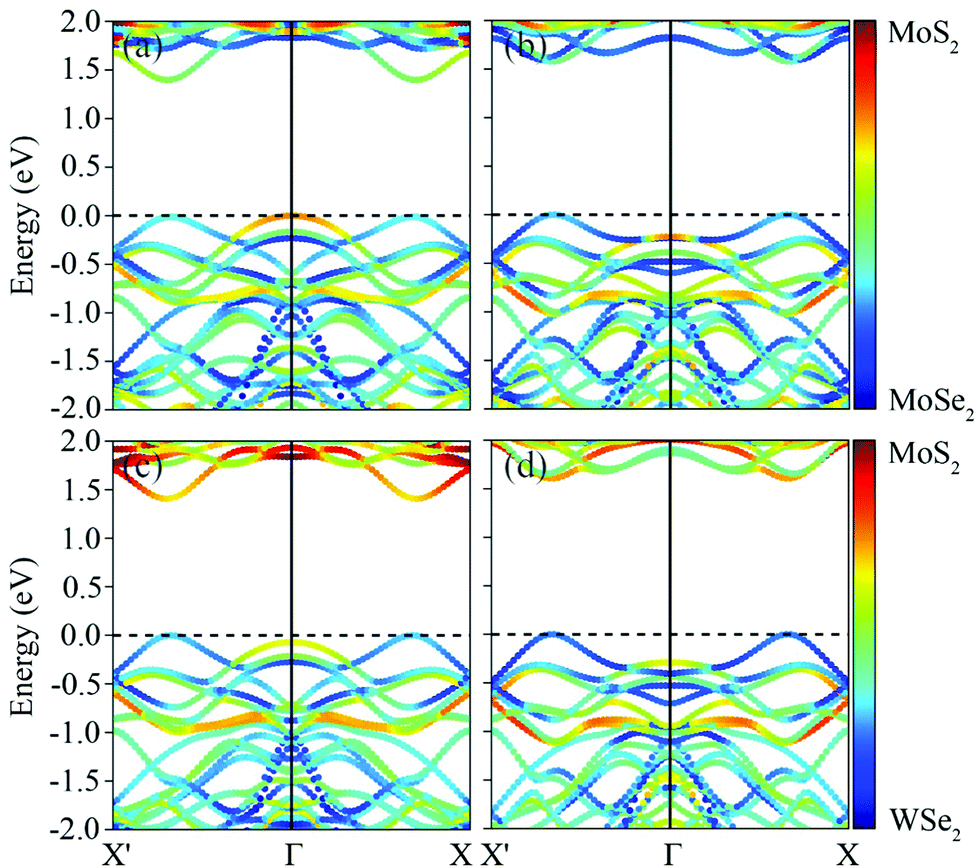 | ||
| Fig. 3 Band structures for (a) MoSe2/MoS2, (b) MoS2/MoSe2, (c) WSe2/MoS2 and (d) MoS2/WSe2 in-plane heterostructures. Fermi level is set to 0. | ||
| E g (eV) | E g-soc (eV) | ΔSOC (meV) | |
|---|---|---|---|
| MoSe2/MoS2 | 1.41 | 1.30 | 175 |
| MoS2/MoSe2 | 1.58 | 1.48 | 172 |
| WSe2/MoS2 | 1.40 | 1.20 | 360 |
| MoS2/WSe2 | 1.61 | 1.40 | 363 |
In Fig. 2(c) of the side view for in-plane heterostructures of 2D TMDs, shadow regions are labeled to refer to the stoichiometric units of constituent TMDs near the interline, from which contributions to the entire band structure are extracted. It should be pointed out that the units near the interline chosen for the projected band structures are sufficient to appreciate the change in contribution to the band structure. As can be noted in Fig. 3(a), electronic states of VBM at the Γ-point are largely attributed to MoS2, which are confirmed by the projected band structures illustrated in Fig. 4. We can also see from Fig. 4 that each MoSe2 (or MoS2) unit on one side of the interline makes unequal contributions to the band edge states, but gradually increases or decreases. An identical phenomenon with MoSe2/MoS2 has been found in the projected band structures of MoS2/MoSe2, as shown in Fig. S3 (ESI†).
 | ||
| Fig. 4 Projected band structures on stoichiometric units of constituent MoSe2 and MoS2. (a–f) Corresponds to numbered shadow regions from 1 to 6. Fermi level is set to 0. | ||
In the cases of MoSe2/MoS2 and MoS2/MoSe2, we can regard the band alignment as type-I to a first approximation. Upon careful inspection of the projected band structures presented in Fig. 4, we can determine that MoSe2 actually makes a larger contribution to CBM at the A-point than MoS2 (53% and 47%, respectively). However, MoSe2 contributes as high as 64% to VBM at the A-point, compared to MoS2 at 36%. As a result, this can be strong evidence for the hybridization states in the in-plane heterostructures near the interline region. In previous works, band alignment of independent 2D MoSe2 and MoS2 has been demonstrated to be type-II,57,58 but without considering interlining effects. We should keep in mind that strong states hybridization occurs over an interline region with a finite length (around 22 Å in our models), and such type-I band alignment is confined within a region not far from the interline. However, states hybridization near the interline will play an important role in determining optical and transport properties and, consequently, impact the application performance of in-plane heterostructures as nanodevices.
With respect to WSe2/MoS2 and MoS2/WSe2, very similar gap values as in the cases of MoSe2/MoS2 and MoS2/MoSe2 are demonstrated, as summarized in Table 2. In contrast, as shown in Fig. 3(c) and (d), the band gaps are direct locating at the A-point. Analogous to MoSe2/MoS2, local structure relaxation causes an indirect–direct band gap crossover in WSe2/MoS2 with the energy difference between VBM at the Γ- and A-point being 67.2 meV, as indicated in Fig. S2 (ESI†). It is interesting that WSe2/MoS2 and MoS2/WSe2 reveal band alignments more like type-II with the VBM located on WSe2 and the CBM on MoS2. In the case of WSe2/MoS2, such a type-II band alignment is verified by the projected band structures shown in Fig. 5. It can be seen that VBM at the A-point is largely composed of WSe2 (67%) in spite of relatively minor states hybridization from MoS2 (33%), while CBM at the A-point is mainly contributed by MoS2 (67%) with a minor contribution from WSe2 (33%). In addition, contributions from both WSe2 and MoS2 to VBM at the A-point gradually decrease when approaching the interline, while the opposite occurs for CBM. In the case of MoS2/WSe2, states hybridization enhances for CBM at the A-point, as shown in Fig. S4 (ESI†). In this section, we point out that a type-II band alignment implies effective spatial separation and accumulation of excitons. As a result, WSe2/MoS2 and MoS2/WSe2 in-plane heterostructures with type-II band alignment suggest the great potential in energy-conversion applications, such as excitonic solar cells. In particular, photon-induced Coulomb drag could probably be realized over the interline region due to the type-II band alignment and significant excitonic effects in MoS2 and WSe2. Coulomb drag is a transport phenomenon whereby long-range Coulomb interaction between charge carriers in two closely spaced but electrically isolated conductors induces voltage in one of the conductors when an electrical current is passed through the other.59 In experiments, for example, Coulomb drag has been realized in bilayer graphene.60,61
 | ||
| Fig. 5 Projected band structures on stoichiometric units of constituent WSe2 and MoS2. (a–f) Correspond to numbered shadow regions from 1 to 6. Fermi level is set to 0. | ||
Amin et al.55 demonstrated that the VBM at Γ-point rises continuously with respect to the VBM at K-point, which can be an explanation for the indirect–direct gap transition in in-plane heterostructures of 2D TMDs. In the case of MoSe2/MoS2, tensile strain is applied to MoS2 and the strained MoS2 will present an indirect band gap. The in-plane MoSe2/MoS2 heterostructure therefore can be regarded as a combination of MoSe2 with a direct band gap and MoS2 with an indirect band gap. As discussed above, MoSe2 and MoS2 contribute almost equally to the VBM at the A-point, and VBM at the Γ-point (deriving mainly from MoS2) is shifted upward with respect to VBM at the A-point. In contrast, in the case of MoS2/MoSe2 a compressive strain is applied to MoSe2 and the strained MoSe2 reveals a direct band gap. In this situation, VBM at the Γ-point is significantly shifted downward in comparison to VBM at the A-point. As a consequence, the indirect–direct band gap transition occurs. However, the upward shift of VBM at the Γ-point in WSe2/MoS2 does not make it higher than VBM at the A-point since the main contributions for VBM at the two points are from different constituents, and a direct band gap at the A-point appears. In addition, when a compressive strain is applied to WSe2 in MoS2/WSe2, VBM at the Γ-point further shifts downward, and thus the direct band gap is maintained. As demonstrated by Amin et al.,55 CBM at the A-point also suffers from significant shift; however, it remains the lowest at the A-point and does not affect our discussion on band gap transition. In the in-plane heterostructures of 2D TMDs, VBM and CBM shifts can also be explained by the effects of bond strength on bonding and antibonding states. In addition, the relative position of VBM at the Γ- and A-point in these in-plane heterostructures of 2D TMDs with intrinsic strain is in close relation to the band edge potential of individual 2D TMD materials.
In the absence of inversion symmetry, energy splitting of the valence band due to SOC effects is a distinct feature of 2D TMDs. It is crucial for understanding optical properties and applications in optoelectronics. As a consequence, knowing how the interline affects spin–orbit splitting is desirable. In these in-plane heterostructures of 2D TMDs considered in this work, the value of SOC strength is also taken from the A-point. In comparison to the energy splitting in constituent TMDs summarized in Table 1, energy splitting for the valence bands of the MoSe2/MoS2 and MoS2/MoSe2 in-plane heterostructures is larger than that of single 2D MoS2 but smaller than that of 2D MoSe2, and comparable with each other, as indicated in Table 2. It is an indication that states hybridization instead of the strain nature has effects on energy splitting. In the cases of WSe2/MoS2 and MoS2/WSe2, energy splitting is also almost the same, which is larger than that of single 2D MoS2 but smaller than that of 2D WSe2. It can be legitimately deduced that the energy splitting values close to those of single 2D WSe2 verifies the main contribution from WSe2 to the valence bands of WSe2/MoS2 and MoS2/WSe2. As we discussed above, the energy splitting in valence bands can reduce the band gap. In both cases of MoSe2/MoS2 and MoS2/MoSe2, band gaps are reduced by approximate 0.1 eV, while 0.2 eV for WSe2/MoS2 and MoS2/WSe2, which reflects the smaller spin–orbit splitting of Mo than that of W. In addition, SOC effects shift the VBM downward at the Γ-point and therefore result in an indirect–direct band gap transition in MoSe2/MoS2, as shown in Fig. S5 in the ESI.† It is an indication that energy splitting induced by SOC effects makes the VBM at A-point shift upward, and it finally surpasses the tensile strain-induced upward shift of the VBM at Γ-point. As a result, the indirect–direct band gap transition occurs due to SOC effects. It should be pointed out that effects of strain and SOC combined determine the band gap nature of in-plane heterostructures of 2D TMDs. In essence, formation of interline between two 2D TMDs averages the energy splitting due to states hybridization.
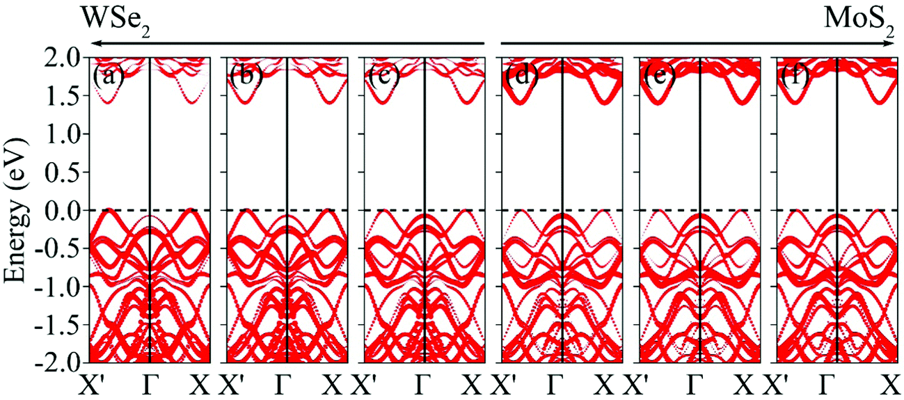
To obtain an in-depth description of the straintronics in the in-plane heterostructures of 2D TMDs, we averaged the lattice constants of the models. It was also acquired in view of the fact that the in-plane heterostructures are grown on the same substrate. In case of MoSe2/MoS2 with averaged lattice constants (referred to as MoSe2/MoS2-a), compressive strain is applied to MoSe2 and tensile strain is applied to MoS2 simultaneously. In this case, VBM at the Γ-point shifts downward and the band structure is characterized in a direct gap at the A-point, as indicated in Fig. 6(a). As summarized in Table 3 of the electronic parameters, the MoSe2/MoS2-a band gap is larger than that of MoSe2/MoS2, while smaller than that of MoS2/MoSe2. The states hybridization persists and the band alignment can be roughly regarded as type-I. In addition, the valence-band energy splitting is almost unchanged in comparison to MoSe2/MoS2 or MoS2/MoSe2, as revealed in Fig. S6 in the ESI.† The situation for WSe2/MoS2 with an averaged lattice constant (referred to as WSe2/MoS2-a) is demonstrated in Table 3 and Fig. 6(b). It still presents a type-II band alignment with VBM and CBM, mainly located on WSe2 and MoS2, respectively. As shown in Table 3 together with Fig. S6 (ESI†), energy splitting due to SOC effects is almost the same as WSe2/MoS2 and MoS2/WSe2. In comparison to MoS2/MoSe2 and MoS2/WSe2, a significant variation in MoSe2/MoS2-a and WSe2/MoS2-a is that CBM at the A-point is degenerate.
 | ||
| Fig. 6 Band structures for (a) MoSe2/MoS2-a and (b) WSe2/MoS2-a in-plane heterostructures with averaged lattice constants. Fermi level is set to 0. | ||
| E g (eV) | E g-soc (eV) | ΔSOC (meV) | |
|---|---|---|---|
| MoSe2/MoS2-a | 1.49 | 1.40 | 173 |
| WSe2/MoS2-a | 1.53 | 1.33 | 355 |
In cases of MoSe2/MoS2-a and WSe2/MoS2-a with average lattice constants, tensile and compressive strain exist simultaneously. Therefore, opposite shift direction of the VBM at the Γ-point competes is indicated. Upon comparing Fig. 3 and 6, it is clear that the energy difference between the VBM at the Γ- and A-point in MoSe2/MoS2-a is larger than that in MoSe2/MoS2, but smaller than that in MoS2/MoSe2. The same situation is true for WSe2/MoS2-a, which supports our discussion on the effects of strain on the shift of band edge states and the reason for indirect–direct band gap transition. In previous studies on the out-of-plane heterostructures of 2D TMDs, such effects of strain on the band structure nature have also been demonstrated from first-principles.62,63 In the MoS2/WSe2 out-of-plane heterostructure with an average lattice constant of constituent monolayers, for example, MoS2 undergoes tensile strain while WSe2 bears compressive strain, and the band structure indicates a direct band gap at the K-point of the hexagonal Brillouin zone.62 In this case, VBM at the K-point is largely contributed by W dxy + dx2−y2 orbitals, while CBM at the K-point is due to the Mo dz2 orbital, and it shows a type-II band alignment. However, the WS2/MoSe2 out-of-plane heterostructure turns out to be an indirect band gap, which is ascribed to the smaller spin–orbit splitting of Mo than that of W. In MoS2/WSe2 and WS2/MoSe2 out-of-plane heterostructures, the energy splitting in valence bands induced by the SOC effects are 460 and 190 meV, respectively.62 It is interesting that the energy splitting values are almost the same as those of individual 2D WSe2 and 2D MoSe2 of 460 and 179 meV (186 meV in this work).63 According to Amin et al.,62 both MoS2/WSe2 and WS2/MoSe2 out-of-plane heterostructures present type-II band alignment; in the case of the former, VBM at the K-point is mainly located on WSe2, and MoSe2 for the latter. In light of the weak van der Waals interlayer interaction, states hybridization between the two constituents is feeble. As a consequence, SOC-induced energy splitting in valence bands in the two out-of-plane heterostructures is almost the same as that in individual constituents. It should be pointed out that strain exists in MoS2/WSe2 and WS2/MoSe2 out-of-plane heterostructures, and the intrinsic strain has almost no effects on spin–orbit splitting, which supports our previous conclusion.
As previously identified, TMDs going from bulk to monolayer results in the transition from indirect to direct band gap, which indicates that interlayer interactions also have influence on band structure nature.64–67 In addition, Kaloni et al.68 suggests that interlayer interaction can also adjust the band structure nature in graphene/TMDs van der Waals heterostructures, where strain also plays a role. An intrinsic electric field can also be established, which is attributed to the charge transfer in the in-plane heterostructures of 2D TMDs with the formation of 1D interlines.69 As suggested by Kaloni et al.,70 the internal electric field can be related with the Löwdin transferred charge through a parallel plate capacitor model. It has been confirmed in silicene-based systems that large amounts of charge transfer provide a large band gap opening. In these in-plane heterostructures of 2D TMDs, therefore, charge transfer across the interlines could also affect the band gap value.
In the in-plane heterostructures of 2D TMDs with intrinsic strain, interlines form and the band gap shows dependency on several factors, as summarized below. In the first place, a difference in the metal d orbital determines the relative position of VBM and CBM. As an important factor, strain shifts the bonding and antibonding state at specific k-points, and further changes the band gap value and nature. The third factor is SOC effects, which shift the VBM at specific high-symmetry k-points and therefore alter the band gap. In addition, states hybridization could affect the shift amplitude of VBM or CBM along with the strain since different 2D TMDs show different resistance to the strain. In the end, charge transfer also plays a role in determining the band gap.
In this section, we calculated formation energy by subtracting the total energies of constituent TMDs from the total energy of the in-plane heterostructure to determine the influence of strain on structure stability. As indicated in Fig. 7, formation energies for MoSe2/MoS2 and WSe2/MoS2 with intrinsic tensile strain are slightly smaller than those of MoS2/MoSe2 and MoS2/WSe2 with intrinsic compressive strain. However, the formation energies are significantly lowered when we averaged lattice constants. In addition, formation energies for in-plane heterostructures with unequal metal atoms are approximately 0.1 eV smaller than those with the same metal atom. In our previous work,69 we obtained very negative formation energies for MoS2/WS2, demonstrating strong covalent bonding, which is free of strain. It is therefore an indication that lattice shrinking or expanding is energy consuming in the in-plane heterostructures with intrinsic strain.
 | ||
| Fig. 7 Formation energy (Ef) for in-plane heterostructures of 2D TMDs considered in this work. | ||
3. Conclusions
In conclusion, we found a direct–indirect band gap transition in 2D TMDs when the applied strain changes from compressive to tensile. In addition, the gap–strain relationship under uniaxial and biaxial strain shows identical behavior, but the band values indicate difference. In the in-plane heterostructures of 2D TMDs with the formation of 1D interlines, strains of a different nature can be introduced within the interline region and significantly influence electronic properties, that is, straintronics. In the current work, we investigated the straintronics in the in-plane heterostructures of 2D TMDs with intrinsic tensile strain, compressive strain, and both tensile and compressive strain. In light of the models of in-plane heterostructures that we proposed, we emphasized the importance of local structure relaxation, which has strong effects on the electronic properties such as indirect–direct band gap crossover. As the nature of intrinsic strain changes, both the band gap value and nature change; for example, the position of band edges can be shifted and indirect–direct band gap crossover occurs. In addition, degeneracy of band edges can also be broken due to intrinsic strain. In general, strain changes nonmetal–metal coupling strength and thus alters the splitting between bonding and antibonding states at a specific k-point, which results in the band gap reduction or enhancement and indirect–direct band gap transition in individual 2D TMDs and in-plane heterostructures of 2D TMDs. In the in-plane heterostructures, intense states hybridization has been found in the interline region, which significantly affects the band alignment of constituent TMDs. It is of interest that states hybridization rather than intrinsic strain influences the energy splitting due to SOC in the valence bands. It should be pointed out that the SOC effects also have substantial effects on the band gap and even causes the indirect–direct band gap transition. In addition, charge transfer across the interline will also affect the band gap, which needs further investigation. In this work, we examined the influence of strain on formation energy, which indicates that lattice shrinking or expanding will reduce bonding strength in these in-plane heterostructures of 2D TMDs. Here, we also note that intrinsic strain could influence the formation of defects and therefore affects the p–n junction behavior of in-plane heterostructures.Acknowledgements
W. Wei thanks Prof. Z. Meng for assistance. This work is financially supported by the National Basic Research Program of China (973 program, 2013CB632401), National Natural Science Foundation of China (11404187, 11374190, 21333006), Taishan Scholar Program of Shandong Province and Fundamental Research Funds of Shandong University.Notes and references
- K. S. Novoselov, A. K. Geim, S. V. Morozov, D. Jiang, Y. Zhang, S. V. Dubonos, I. V. Grigorieva and A. A. Firsov, Science, 2004, 306, 666–669 CrossRef CAS PubMed.
- J. N. Coleman, M. Lotya, A. O'Neill, S. D. Bergin, P. J. King, U. Khan, K. Young, A. Gaucher, S. De, R. J. Smith, I. V. Shvets, S. K. Arora, G. Stanton, H.-Y. Kim, K. Lee, G. T. Kim, G. S. Duesberg, T. Hallam, J. J. Boland, J. J. Wang, J. F. Donegan, J. C. Grunlan, G. Moriarty, A. Shmeliov, R. J. Nicholls, J. M. Perkins, E. M. Grieveson, K. Theuwissen, D. W. McComb, P. D. Nellist and V. Nicolosi, Science, 2011, 331, 568–571 CrossRef CAS PubMed.
- M. Chhowalla, H. S. Shin, G. Eda, L.-J. Li, K. P. Loh and H. Zhang, Nat. Chem., 2013, 5, 263–275 CrossRef PubMed.
- X. Qian, J. Liu, L. Fu and J. Li, Science, 2014, 346, 1344–1347 CrossRef CAS PubMed.
- Z. Y. Zhu, Y. C. Cheng and U. Schwingenschlögl, Phys. Rev. B: Condens. Matter Mater. Phys., 2011, 84, 153402 CrossRef.
- A. Ramasubramaniam, Phys. Rev. B: Condens. Matter Mater. Phys., 2012, 84, 115409 CrossRef.
- K. F. Mak, C. Lee, J. Hone, J. Shan and T. F. Heinz, Phys. Rev. Lett., 2010, 105, 136805 CrossRef PubMed.
- C.-C. Wu, D. Jariwala, V. K. Sangwan, T. J. Marks, M. C. Hersam and L. J. Lauhon, J. Phys. Chem. Lett., 2013, 4, 2508–2513 CrossRef CAS.
- A. Gupta, V. Arunachalam and S. Vasudevan, J. Phys. Chem. Lett., 2015, 6, 739–744 CrossRef CAS PubMed.
- H. S. Ahn and A. J. Bard, J. Phys. Chem. Lett., 2016, 7, 2748–2752 CrossRef CAS PubMed.
- A. Splendiani, L. Sun, Y. Zhang, T. Li, J. Kim, C.-Y. Chim, G. Galli and F. Wang, Nano Lett., 2010, 10, 1271–1275 CrossRef CAS PubMed.
- B. Radisavljevic, A. Radenovic, J. Brivio, V. Giacometti and A. Kis, Nat. Nanotechnol., 2011, 6, 147–150 CrossRef CAS PubMed.
- B. Radisavljevic, M. B. Whitwick and A. Kis, ACS Nano, 2011, 5, 9934–9938 CrossRef CAS PubMed.
- Z. Yin, H. Li, H. Li, L. Jiang, Y. Shi, Y. Sun, G. Lu, Q. Zhang, X. Chen and H. Zhang, ACS Nano, 2012, 6, 74–80 CrossRef CAS PubMed.
- D. Xiao, G.-B. Liu, W. Feng, X. Xu and W. Yao, Phys. Rev. Lett., 2012, 108, 196802 CrossRef PubMed.
- L. Sun, J. Yan, D. Zhan, L. Liu, H. Hu, H. Li, B. K. Tay, J.-L. Kuo, C.-C. Huang, D. W. Hewak, P. S. Lee and Z. X. Shen, Phys. Rev. Lett., 2013, 111, 126801 CrossRef PubMed.
- L. Kou, T. Frauenheim and C. Chen, J. Phys. Chem. Lett., 2013, 4, 1730–1736 CrossRef CAS PubMed.
- R. Long and O. V. Prezhdo, Nano Lett., 2016, 16, 1996–2003 CrossRef CAS PubMed.
- S. Tongay, W. Fan, J. Kang, J. Park, U. Koldemir, J. Suh, D. S. Narang, K. Liu, J. Ji, J. Li, R. Sinclair and J. Wu, Nano Lett., 2014, 14, 3185–3190 CrossRef CAS PubMed.
- X. Zhu, N. R. Monahan, Z. Gong, H. Zhu, K. W. Williams and C. A. Nelson, J. Am. Chem. Soc., 2015, 137, 8313–8320 CrossRef CAS PubMed.
- C.-H. Lee, G.-H. Lee, A. M. van der Zande, W. C. Chen, Y. L. Li, M. Y. Han, X. Cui, G. Arefe, C. Nuckolls, T. F. Heinz, J. Guo, J. Hone and P. Kim, Nat. Nanotechnol., 2014, 9, 676–681 CrossRef CAS PubMed.
- L. Ci, L. Song, C. Jin, D. Jariwala, D. Wu, Y. Li, A. Srivastava, Z. F. Wang, K. Storr, L. Balicas, F. Liu and P. M. Ajayan, Nat. Mater., 2010, 9, 430–435 CrossRef CAS PubMed.
- T. P. Kaloni, R. P. Joshi, N. P. Adhikari and U. Schwingenschlögl, Appl. Phys. Lett., 2014, 104, 073116 CrossRef.
- R. Martinez-Gordillo and M. Pruneda, Phys. Rev. B: Condens. Matter Mater. Phys., 2015, 91, 045411 CrossRef.
- J. M. Pruneda, Phys. Rev. B: Condens. Matter Mater. Phys., 2012, 85, 045422 CrossRef.
- J. M. Pruneda, Phys. Rev. B: Condens. Matter Mater. Phys., 2010, 81, 161409 CrossRef.
- P. Srivastava, M. Deshpande and P. Sen, Phys. Chem. Chem. Phys., 2011, 13, 21593–21599 RSC.
- J. He, K.-Q. Chen, Z.-Q. Fan, L.-M. Tang and W. P. Hu, Appl. Phys. Lett., 2010, 97, 193305 CrossRef.
- Q. Sun, Y. Dai, Y. Ma, W. Wei and B. Huang, RSC Adv., 2015, 5, 33037–33043 RSC.
- K. Bogaert, S. Liu, J. Chesin, D. Titow, S. Gradečak and S. Garaj, Nano Lett., 2016, 16, 5129–5134 CrossRef CAS PubMed.
- Y. Yoo, Z. P. Degregorio and J. E. Johns, J. Am. Chem. Soc., 2015, 137, 14281–14287 CrossRef CAS PubMed.
- K. Chen, X. Wan, J. Wen, W. Xie, Z. Kang, X. Zeng, H. Chen and J.-B. Xu, ACS Nano, 2015, 9, 9868–9876 CrossRef CAS PubMed.
- X.-Q. Zhang, C.-H. Lin, Y.-W. Tseng, K.-H. Huang and Y.-H. Lee, Nano Lett., 2015, 15, 410–415 CrossRef CAS PubMed.
- K. Chen, X. Wan, W. Xie, J. Wen, Z. Kang, X. Zeng, H. Chen and J. Xu, Adv. Mater., 2015, 27, 6431–6437 CrossRef CAS PubMed.
- Y. Gong, J. Lin, X. Wang, G. Shi, S. Lei, Z. Lin, X. Zou, G. Ye, R. Vajtai, B. I. Yakobson, H. Terrones, M. Terrones, B. K. Tay, J. Lou, S. T. Pantelides, Z. Liu, W. Zhou and P. M. Ajayan, Nat. Mater., 2014, 13, 1135–1142 CrossRef CAS PubMed.
- C. Huang, S. Wu, A. M. Sanchez, J. J. P. Peters, R. Beanland, J. S. Ross, P. Rivera, W. Yao, D. H. Cobden and X. Xu, Nat. Mater., 2014, 13, 1096–1101 CrossRef CAS PubMed.
- Y. Gong, S. Lei, G. Ye, B. Li, Y. He, K. Keyshar, X. Zhang, Q. Wang, J. Lou, Z. Liu, R. Vajtai, W. Zhou and P. M. Ajayan, Nano Lett., 2015, 15, 6135–6141 CrossRef CAS PubMed.
- M. Mahjouri-Samani, M.-W. Lin, K. Wang, A. R. Lupini, J. Lee, L. Basile, A. Boulesbaa, C. M. Rouleau, A. A. Puretzky, I. N. Ivanov, K. Xiao, M. Yoon and D. B. Geohegan, Nat. Commun., 2015, 6, 7749 CrossRef CAS PubMed.
- X. Duan, C. Wang, J. C. Shaw, R. Cheng, Y. Chen, H. Li, X. Wu, Y. Tang, Q. Zhang, A. Pan, J. Jiang, R. Yu, Y. Huang and X. Duan, Nat. Nanotechnol., 2014, 9, 1024–1030 CrossRef CAS PubMed.
- M.-Y. Li, Y. Shi, C.-C. Cheng, L.-S. Lu, Y.-C. Lin, H. L. Tang, M.-L. Tsai, C.-W. Chu, K.-H. Wei, Jr., H. He, W.-H. Chang, K. Suenaga and L.-J. Li, Science, 2015, 349, 524–528 CrossRef CAS PubMed.
- J. Kang, H. Sahin and F. M. Peeters, J. Phys. Chem. C, 2015, 119, 9580–9586 CAS.
- G. Kresse and J. Furthmuller, Phys. Rev. B: Condens. Matter Mater. Phys., 1996, 54, 11169 CrossRef CAS.
- G. Kresse and J. Joubert, Phys. Rev. B: Condens. Matter Mater. Phys., 1999, 59, 1758 CrossRef CAS.
- J. P. Perdew, K. Burke and M. Ernzerhof, Phys. Rev. Lett., 1996, 77, 3865 CrossRef CAS PubMed.
- J. P. Perdew and Y. Wang, Phys. Rev. B: Condens. Matter Mater. Phys., 1992, 45, 13244 CrossRef.
- H. J. Monkhorst and J. D. Pack, Phys. Rev. B: Solid State, 1976, 13, 5188 CrossRef.
- S.-H. Lin and J.-L. Kuo, Phys. Chem. Chem. Phys., 2015, 17, 29305–29310 RSC.
- H. Li, M. Huang and G. Cao, Phys. Chem. Chem. Phys., 2016, 18, 15110–15117 RSC.
- B. Rajbanshi, S. Sarkar and P. Sarkar, Phys. Chem. Chem. Phys., 2015, 17, 26166–26174 RSC.
- W. Huang, X. Luo, C. K. Gan, S. Y. Quek and G. Liang, Phys. Chem. Chem. Phys., 2014, 16, 10866–10874 RSC.
- Y. Ma, Y. Dai, M. Guo, C. Niu, J. Lu and B. Huang, Phys. Chem. Chem. Phys., 2011, 13, 15546–15553 RSC.
- H. Peelaers and C. G. Van de Walle, Phys. Rev. B: Condens. Matter Mater. Phys., 2012, 86, 241401 CrossRef.
- M. Ghorbani-Asl, S. Borini, A. Kuc and T. Heine, Phys. Rev. B: Condens. Matter Mater. Phys., 2013, 87, 235434 CrossRef.
- P. Johari and V. B. Shenoy, ACS Nano, 2012, 6, 5449–5456 CrossRef CAS PubMed.
- B. Amin, T. P. Kaloni and U. Schwingenschlögl, RSC Adv., 2014, 4, 34561–34565 RSC.
- Y. Li, Z. Zhou, S. Zhang and Z. Chen, J. Am. Chem. Soc., 2008, 130, 16739–16744 CrossRef CAS PubMed.
- J. Kang, S. Tongay, J. Zhou, J. Li and J. Wu, Appl. Phys. Lett., 2013, 102, 012111 CrossRef.
- Y. Guo and J. Robertson, Appl. Phys. Lett., 2016, 108, 233104 CrossRef.
- B. N. Narozhny and A. Levchenko, Rev. Mod. Phys., 2016, 88, 025003 CrossRef.
- S. Kim, I. Jo, J. Nah, Z. Yao, S. K. Banerjee and E. Tutuc, Phys. Rev. B: Condens. Matter Mater. Phys., 2011, 83, 161401 CrossRef.
- J. I. A. Li, T. Taniguchi, K. Watanabe, J. Hone, A. Levchenko and C. R. Dean, Phys. Rev. Lett., 2016, 117, 046802 CrossRef CAS PubMed.
- B. Amin, T. P. Kaloni, G. Schreckenbach and M. S. Freund, Appl. Phys. Lett., 2016, 108, 063105 CrossRef.
- B. Amin, N. Singh and U. Schwingenschlögl, Phys. Rev. B: Condens. Matter Mater. Phys., 2015, 92, 075439 CrossRef.
- Y. Ma, Y. Dai, M. Guo, C. Niu, J. Lu and B. Huang, Phys. Chem. Chem. Phys., 2011, 13, 15546–15553 RSC.
- L. Sun, J. Yan, D. Zhan, L. Liu, H. Hu, H. Li, B. K. Tay, J.-L. Kuo, C.-C. Huang, D. W. Hewak, P. S. Lee and Z. X. Shen, Phys. Rev. Lett., 2013, 111, 126801 CrossRef PubMed.
- K. F. Mak, C. Lee, J. Hone, J. Shan and T. F. Heinz, Phys. Rev. Lett., 2010, 105, 136805 CrossRef PubMed.
- Y. Ma, Y. Dai, M. Guo, C. Niu and B. Huang, Nanoscale, 2011, 3, 3883–3887 RSC.
- T. P. Kaloni, L. Kou, T. Frauenheim and U. Schwingenschlögl, Appl. Phys. Lett., 2014, 105, 233112 CrossRef.
- W. Wei, Y. Dai and B. Huang, Phys. Chem. Chem. Phys., 2016, 18, 15632–15638 RSC.
- T. P. Kaloni, G. Schreckenbach and M. S. Freund, J. Phys. Chem. C, 2014, 118, 23361–23367 CAS.
Footnote |
| † Electronic supplementary information (ESI) available. See DOI: 10.1039/c6cp07823k |
| This journal is © the Owner Societies 2017 |