
4 nm ZnO nanocrystals fabrication through electron beam irradiation on the surface of a ZnO nanoneedle formed by thermal annealing†
Jian-Min
Li
Department of Physics, Zhejiang University, Hangzhou 310027, People's Republic of China. E-mail: phyjmli@zju.edu.cn
First published on 23rd November 2016
Abstract
A vertically-oriented growth of the monolithic ZnO nanocrystals (NCs)-on-nanoneedle (NN) single-crystalline (SC) hybrids is presented with intrinsic nanoscale complexity, consisting of spatially homogeneously distributed ultrahigh-density (2.0 × 104 μm−2) on-site homoepitaxial growth of 4 nm ZnO NCs on the surface of vertically oriented high-density (8 × 108 cm−2) SC [10![[1 with combining macron]](https://www.rsc.org/images/entities/char_0031_0304.gif) 0] ZnO NNs. The electron-beam stimulated “self-additive on-surface oxidation-limited growth” at room temperature is proposed for the on-site growth of numerous ZnO NCs on the (0001) facets of a single ZnO NN. Compared with heterojunctions, the unprecedented compact monolithic ZnO NCs-on-NN SC hybrids, growing from the inside out, may hold great promise for enhanced photovoltaic performance (e.g., electron mobility) of ZnO NC-sensitized solar cells.
0] ZnO NNs. The electron-beam stimulated “self-additive on-surface oxidation-limited growth” at room temperature is proposed for the on-site growth of numerous ZnO NCs on the (0001) facets of a single ZnO NN. Compared with heterojunctions, the unprecedented compact monolithic ZnO NCs-on-NN SC hybrids, growing from the inside out, may hold great promise for enhanced photovoltaic performance (e.g., electron mobility) of ZnO NC-sensitized solar cells.
Nowadays, the ever-increasing miniaturization of devices continues to increase the structural complexity and functional integration of nanomaterials,1,2e.g., microtetrapod-on-nanowire (NW) hybrids3 and complicated micro-nanocrystal tetrapods.4 Vertically oriented one-dimensional (1-D) NWs are becoming critical for enhanced efficiency in photovoltaics and photodetectors owing to their exposed large surface-to-volume ratio.5–8 Due to their multi-functional properties, in particular piezoelectricity, standing-up II–VI direct compound semiconductor zinc oxide (ZnO) NWs have been identified as important components of piezoelectric nanogenerators for future self-powered nanosystems.9,10 On the other hand, due to the quantum confinement effect,11 zero-dimensional (0-D) semiconductor nanocrystals or quantum dots (QDs) provide numerous possibilities in optoelectronic devices (including LEDs and solar cells) and biological imaging.12 Generally, building uniquely integrated nanodevices or hybrid nanocrystals could take advantage of 0-D and 1-D nanostructures together. In order to boost light harvesting and fast electron transportation, vertically aligned NWs coated with QDs were specifically designed for energy scavenging.13 Such material design could not only increase the density of devices, but also combine the advantageous optoelectronic and piezoelectric properties of the individual components and exhibit novel superior properties that may be attributed to cooperative effects. Compared with nanocomposite structures, single-crystalline (SC) solids in principle have the best performance. As a perfect combination, construction of monolithic 0-D QD-on-1-D NW SC hybrids represents a highly integrated and compact conceptual framework with advantages over existing solutions for maximizing the efficiency of advanced energy conversion-and-storage applications such as most promising high-efficiency photoanodes. However, the practical realization of integration of 0-D QDs with 1-D NWs is still a great long-standing nanotechnology challenge due to the inevitable coalescence and thermal instability of 0-D QDs: first, the coalescence or aggregation of QDs is often inevitable, resulting in deteriorating performance. Most QDs are prepared by “wet” chemistry methods, i.e., solution-processed colloidal QDs in organic media, which require a tough solvent removal processing scheme. Thus, developing new “dry” strategies for the eco-friendly QDs is highly desirable. Second, most of the investigated LED phosphor QDs are cadmium-based.14 As a less toxic alternative to cadmium-free QDs,15 ZnO is an excellent candidate for environment-friendly “green” nanomaterial in 3rd generation QD-sensitized solar cells (QDSSCs or Gratzel solar cells).16–18 Finally, the central challenge of advanced materials is the controllable growth and fabrication of given structures or components at a given localization for given functions. The new clean technology should also facilitate delicate nanomanufacture where QDs could be densely integrated with SC NWs precisely.
Here, we demonstrate a feasible approach to integration of ultrahigh-density (2.0 × 104 μm−2) monolithic ZnO 4 nm nanocrystals (NCs) homoepitaxially grown on the surface of vertically oriented high-density (8 × 108 cm−2) nanoneedles (NNs) or nanopillars by a combination of zinc (Zn) foil thermal oxidation and electron beam irradiation (EBI). The monolithic ZnO 0-D NC-on-1-D NN SC hybrid fabrication process comprises two steps: (i) to grow [100] SC ZnO NNs directly by thermal oxidation of pure Zn foils, and (ii) then subsequently use a single [100] SC ZnO NN to generate on-site growth of 4 nm ZnO NCs on (0001) facets of the vertically oriented SC ZnO NN enabled by EBI. This strategy presents a scalable, “dry”, internal oxidation method of vertically oriented growth of monolithic ZnO NC-on-NN SC hybrids without post-solvent removal treatment—an ability not available by any chemical means.
A piece of cold-rolled metallic Zn foil (purity, 99.9%) was slowly heated (3 K min−1) up to 948 K for 24 h under ambient conditions (in a horizontal tubular electric furnace with two ends open to the atmosphere), and subsequently naturally cooled down to room temperature (RT). By this simple approach, the initial silver-colored smooth Zn foil becomes dark gray with a “rugged” topography (inset in Fig. 1a). When looking closely at the image of this as-grown product on the roughening surface of the Zn foils using a high-magnification scanning electron microscope (SEM), one sees dense grass-like NW or NN arrays with a sharp-tip morphology, of approximately 60–180 nm in diameter (Fig. 1b). The cross-sectional SEM image indicates that the NNs of up to 10 μm in length (a high aspect-ratio >100) are quasi-vertically oriented with respect to the substrate surface of the Zn foils (Fig. 1c). The area density of the ZnO NN surface was estimated to be 8 × 108 cm−2 by counting the NNs in the SEM images. It deserves mention here that by using low-cost equipment, the Zn foil thermal oxidation is the easiest method to achieve vertically oriented growth of large-scale ZnO NNs directly on Zn foils where the top Zn layers were oxidized into ZnO.
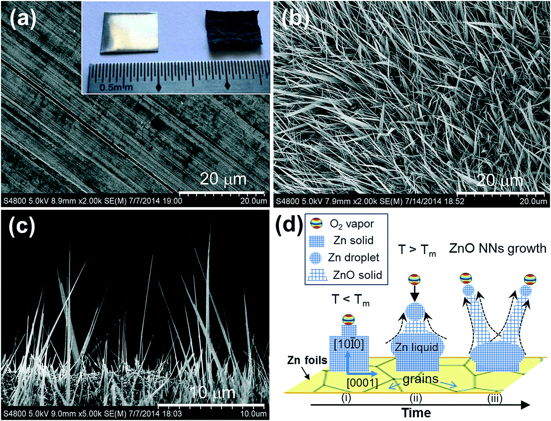 | ||
| Fig. 1 (a) Scanning electron microscopy (SEM) image of highly surface-textured cold-rolled Zn foils at the beginning. Inset in (a): comparison of digital photographs before (left)/after (right) oxidation indicate the strong surface roughening of ZnO NNs on Zn foil. (b) Plane-view SEM image of ZnO NNs grown on Zn foils. (c) Side-view SEM image of ZnO NN arrays grown on Zn foils. (d) A schematic representation showing the “self-catalytic creeping VLS growth” mechanism of vertically aligned ZnO NNs on a Zn foil substrate. | ||
Recently, the thermal oxidation of Zn foil to form nanowires was also reported; however, the underlying growth mechanism remains unclear.19 How do ZnO NNs spontaneously grow through thermal oxidation of pure Zn foils in air? First, the actual oxidation process of metallic Zn occurs even at the low temperature of 653 K, below its melting-point (Tm = 692 K).20 Similar to the previous catalyst-assisted vapor-phase transport,21,22 the ZnO NWs result from oxidation of Zn foils with an O2 vapor source, Zn + O2 ⇒ ZnO. Upon heating of the Zn foils at a temperature below 948 K, the top Zn layers react with O2 from the atmosphere, and may already oxidize into ZnO “grain stems” as “seeding” nanocatalysts. Second, the optimal growth temperature (948 K) is above the Tm of the Zn substrate, i.e., Zn would be in the liquid state, a vapor–solid (VS) growth mode could be excluded. Third, due to ZnO NNs with no catalyst tipped, the main evidence of the widely used vapor–liquid–solid (VLS) route for 1-D nanostructure growth,23,24 a regular VLS mechanism is unlikely at work as well. At temperatures above Tm, Zn small liquid droplets will “creep” along the surfaces of the ZnO “grain stems” and then diffuse up to the top of the growth front of a NW. Note that a liquid Zn droplet is creeping or moving during growth rather than being fixed. As shown in Fig. 1d, a novel mechanism called “self-catalytic creeping VLS mechanism” is therefore proposed for promoting ZnO NN growth at elevated temperatures, instead of the VS mode. The Zn liquid phase itself plays a pivotal catalyst role in mediating mass transport from the root to the growth front of a NW. This self-catalytic ZnO NN growth process is sustained to a certain length until creeping Zn droplets oxidize completely. In the thermal oxidation process, transport of the Zn droplets onto the growth front of a NW is controlled by the competition between oxidation and the upward-diffusion velocity of Zn. During the Zn transportation, the droplets will oxidize and creep simultaneously. Thus the droplet is becoming smaller with the decelerated growth rate of the tipping, resulting in ZnO NNs with a tapered growth geometry. Because the surface energy (509 ergs cm−2) of Zn basal planes {0001} is lower (763.5 ergs cm−2) than that of {100} planes,25 as the oxidation process proceeds, the ZnO will nucleate and grow along the [100] direction in 1D nanostructures.
Except for a few Zn peaks (red, JCPDS no. 65-3358) from the residual Zn foils underneath as supporting substrate (Fig. 2a), all the recorded powder X-ray diffraction (PXRD) peaks can be readily indexed to the hexagonal wurtzite-type (WZ) structure of the ZnO phase (JCPDS no. 36-1451). A strong and sharp (100) or (100) diffraction peak in the as-grown sample suggests that a re-orientation of Zn texture was found from the original [002] or [0001] to the [100] growth direction (the blue arc arrow is drawn to guide the eye). During thermal oxidation. As a template, the vertical orientation [100] of Zn nanocrystal facet exposure out of the (0002) Zn foils would induce the ZnO NN vertical growth on Zn foils during the thermal oxidation. As shown in Fig. 2b, both our samples and commercial ZnO powders (purity, 99.999%) exhibit six Raman peaks at 99.6 cm−1 (E2(low)), 437.8 cm−1 (E2(high)), 409.6 cm−1 (E1(TO)), 378.6 cm−1 (A1(TO)), 332.1 cm−1 (E2 − E1), and 1153.3 cm−1 (the second order vibration (2LO)) modes of ZnO WZ structure.26–28 The E1(LO) mode peak at 583.2 cm−1 in bulk ZnO indicates that there are oxygen vacancies (Vo) in the ZnO NNs.28 An intense new low-wavenumber Raman-active line, centered at 71.2 cm−1 (the black arrow is drawn to guide the eye), was observed for ZnO NNs when compared with that of commercial ZnO powders. Presently the reason is still unknown, probably due to defect-related symmetry breaking of ZnO. The photoluminescence (PL) spectrum of the ZnO NNs exhibits a medium near-band-edge emission at 379.8 nm in the ultraviolet (UV) and a broad green emission at 506.7 nm (Fig. 2c). The green emission is usually attributed to defect emissions such as oxygen deficiency, manifested in the form of Vo or zinc interstitials (Zni) in ZnO.29 The PL spectrum was fitted with eight Gaussian-type peaks at 466 nm (VZn−), 485 nm (VoOi), 510 nm (Vo1), 521 nm (OZn), 544 nm (O0i), 574 nm (VoZn), 620 nm (Vo+), and 765 nm (Vo).30–32 Additionally, X-ray photoelectron spectroscopy (XPS) measurement on our ZnO NNs (Fig. 2d) indicated that the O1s peak fittings were fitted using two individual subpeaks at 531.1 eV (the blue arrow guides the eyes), and 532.9 eV (the green arrow guides the eyes), respectively. The recent work indicates that O1s at 531.1 eV was considered as evidence of the existence of oxygen deficiency.33,34 The dominant percentage of the oxygen deficiency-related defect components was estimated to be ∼59.4%. It is well known that Zn and ZnO have the same crystal structure (hexagonal close packed, hcp) but with different lattice parameters for Zn: a = b = 2.67 Å, c = 4.95 Å, and ZnO: a = b = 3.25 Å, c = 5.21 Å. Both the above-mentioned high surface energy of {100} planes and the low lattice mismatch (4.8%) between Zn/ZnO interfaces along the prism plane [100] favor the preferential interface nucleation-and-growth of continuous ZnO NNs over the Zn surface.35 Lastly, due to a large thermal expansion coefficient mismatch between Zn and ZnO, the growth of ZnO NNs is inclined, tilted or canted with the substrate surface when the growth has finished, which is responsible for the “rugged” solid surface in the final morphology.
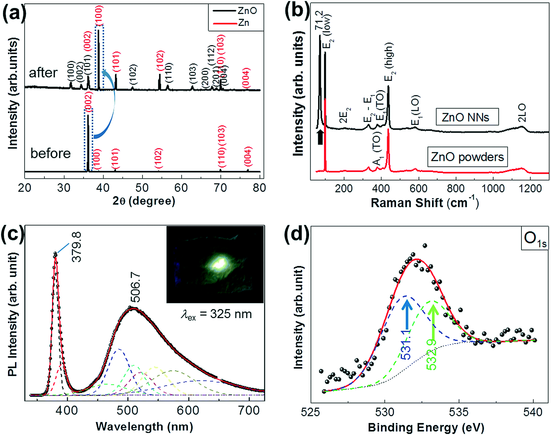 | ||
| Fig. 2 (a) PXRD patterns with CuKα radiation obtained from ZnO NNs grown on Zn foils (before and after growth for comparison). (b) RT Raman spectrum of the ZnO NNs on Zn foils using a 532 nm laser. (c) PL (Edinburgh Instruments FLS920) spectra of stimulated emission in ZnO NNs measured at RT. (d) Fitting of O1s core-level XPS spectra of the ZnO NNs. The background (dashed black lines) was removed using the standard Shirley subtraction method. The peak fittings were performed using a pure Gaussian function. The dotted lines and arrows are drawn to guide the eye. | ||
After heavy ultrasonic treatment of the ZnO NNs grown on Zn foils using a probe sonicator (Misonix S-4000), a drop of the liquid containing the ZnO NNs was sprayed onto a holey carbon copper grid for high-resolution transmission electron microscopy (HRTEM) (FEI, TECANAL G2 F20) microstructure characterization. A representative HRTEM image reveals that the NN is SC in nature (Fig. 3d), and the adjacent lattice planes were about 2.53 Å apart, corresponding to the distance between two (0002) crystal planes of WZ ZnO. This shows that the SC ZnO NNs arrays are grown on Zn foils along the [100] direction and enclosed by (0001) facets, which is different from the arrayed [0001] ZnO NWs grown from aqueous solutions.36 Intriguingly, the SC ZnO NNs were found to be easily damaged when subjected to focused EBI (settings, magnification: 590 kx, spot size: 1, dose: 14![[thin space (1/6-em)]](https://www.rsc.org/images/entities/char_2009.gif) 800 e Å−2 s−1) even for one minute. Representative close-up serial HRTEM images show surface morphology evolution for a single ZnO NN by the EBI process with time increasing to 4 min (Fig. 3b–d). A striking feature was observed, that a massive amount of NCs start to precipitate from the ZnO NN parent phases (the arrows are drawn to guide the eye) and spatially homogeneously distributed on the surface of the SC ZnO NN. Remarkably, the growth of ZnO QDs is self-additive and non-injection, and the ZnO NCs are well separated and “built-in” on the ZnO NN (Fig. 3d), avoiding the coalescence of NCs. The SAED pattern of NC-on-NN hybrids indicates that the compact ZnO SC hybrid has the same SC structure as that of the initial ZnO NN (inset in Fig. 3e), suggesting a homoepitaxial growth of high-quality monolithic ZnO NC-on-NN SC hybrids. Namely, the numerous well-isolated 0-D ZnO NCs combined with a single 1-D ZnO NN self-assembled into a new level of more complex nanoarchitecture. The average diameter statistics of the ZnO QDs are about 4 nm made with 102 ZnO NCs (Fig. 3f), which is close to that of chemically synthesized colloidal ZnO QDs.37 The area density of the ZnO NC on-site homoepitaxial growth on the single vertically oriented SC ZnO NN was estimated to be 2.0 × 104 μm−2 by counting NCs in the TEM images, implying an ultrahigh-density nucleation-and-growth, which is attractive for high-performance QDSSCs and field emission applications. More HRTEM images of the ultrahigh-density ZnO NC homoepitaxial growth on another ZnO NN are given in Fig. 4, showing the excellent reproducibility. Furthermore, under EBI, the on-site homoepitaxial growth of NCs on the surface of an individual ZnO NN was investigated by in situ TEM technique at RT (Video S1†).
800 e Å−2 s−1) even for one minute. Representative close-up serial HRTEM images show surface morphology evolution for a single ZnO NN by the EBI process with time increasing to 4 min (Fig. 3b–d). A striking feature was observed, that a massive amount of NCs start to precipitate from the ZnO NN parent phases (the arrows are drawn to guide the eye) and spatially homogeneously distributed on the surface of the SC ZnO NN. Remarkably, the growth of ZnO QDs is self-additive and non-injection, and the ZnO NCs are well separated and “built-in” on the ZnO NN (Fig. 3d), avoiding the coalescence of NCs. The SAED pattern of NC-on-NN hybrids indicates that the compact ZnO SC hybrid has the same SC structure as that of the initial ZnO NN (inset in Fig. 3e), suggesting a homoepitaxial growth of high-quality monolithic ZnO NC-on-NN SC hybrids. Namely, the numerous well-isolated 0-D ZnO NCs combined with a single 1-D ZnO NN self-assembled into a new level of more complex nanoarchitecture. The average diameter statistics of the ZnO QDs are about 4 nm made with 102 ZnO NCs (Fig. 3f), which is close to that of chemically synthesized colloidal ZnO QDs.37 The area density of the ZnO NC on-site homoepitaxial growth on the single vertically oriented SC ZnO NN was estimated to be 2.0 × 104 μm−2 by counting NCs in the TEM images, implying an ultrahigh-density nucleation-and-growth, which is attractive for high-performance QDSSCs and field emission applications. More HRTEM images of the ultrahigh-density ZnO NC homoepitaxial growth on another ZnO NN are given in Fig. 4, showing the excellent reproducibility. Furthermore, under EBI, the on-site homoepitaxial growth of NCs on the surface of an individual ZnO NN was investigated by in situ TEM technique at RT (Video S1†).
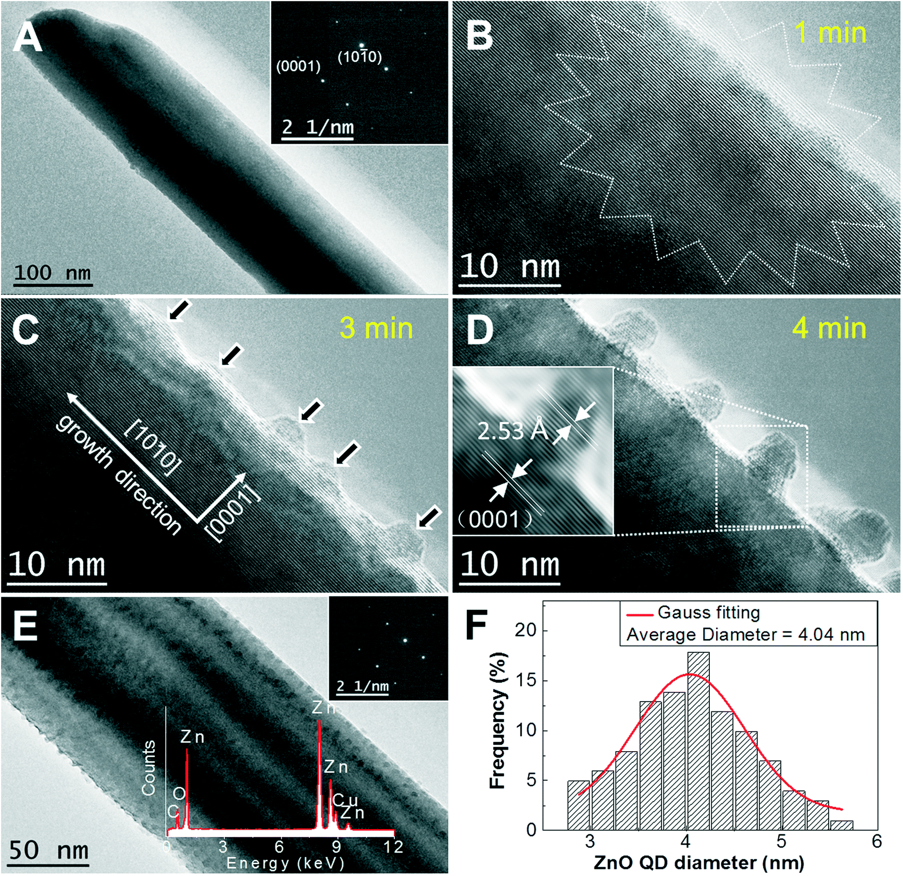 | ||
| Fig. 3 (a) Initial TEM image of an individual ZnO NN. Inset: its corresponding selected area electron diffraction (SAED) pattern confirming the growth of ZnO NNs along the [100] direction of WZ ZnO. (b–d) A series of HRTEM images of a single [100] ZnO NN under EBI at different irradiation times. The white star circle in (b) guides the eyes for variations in the EBI region. Inset in (d): corresponding enlarged simulated HRTEM image of the white dashed box area shown in (d) indicates the on-site homoepitaxial growth of numerous NCs on (0001) facets on the [100] direction of WZ ZnO NNs. (e) HRTEM image of ultrahigh-density 4 nm ZnO NC on-site homoepitaxial growth on an individual SC ZnO NN. Inset, bottom: a representative EDAX pattern collected from an individual NC-on-NN hybrid indicating that the hybrid is pure ZnO. The tiny Cu peak came from the TEM grid. (f) The diameter distribution of the ZnO NCs on the surface of a ZnO NN, showing the very homogenous distribution. The diameter (red line) from TEM images was fitted using a pure Lorentzian function. | ||
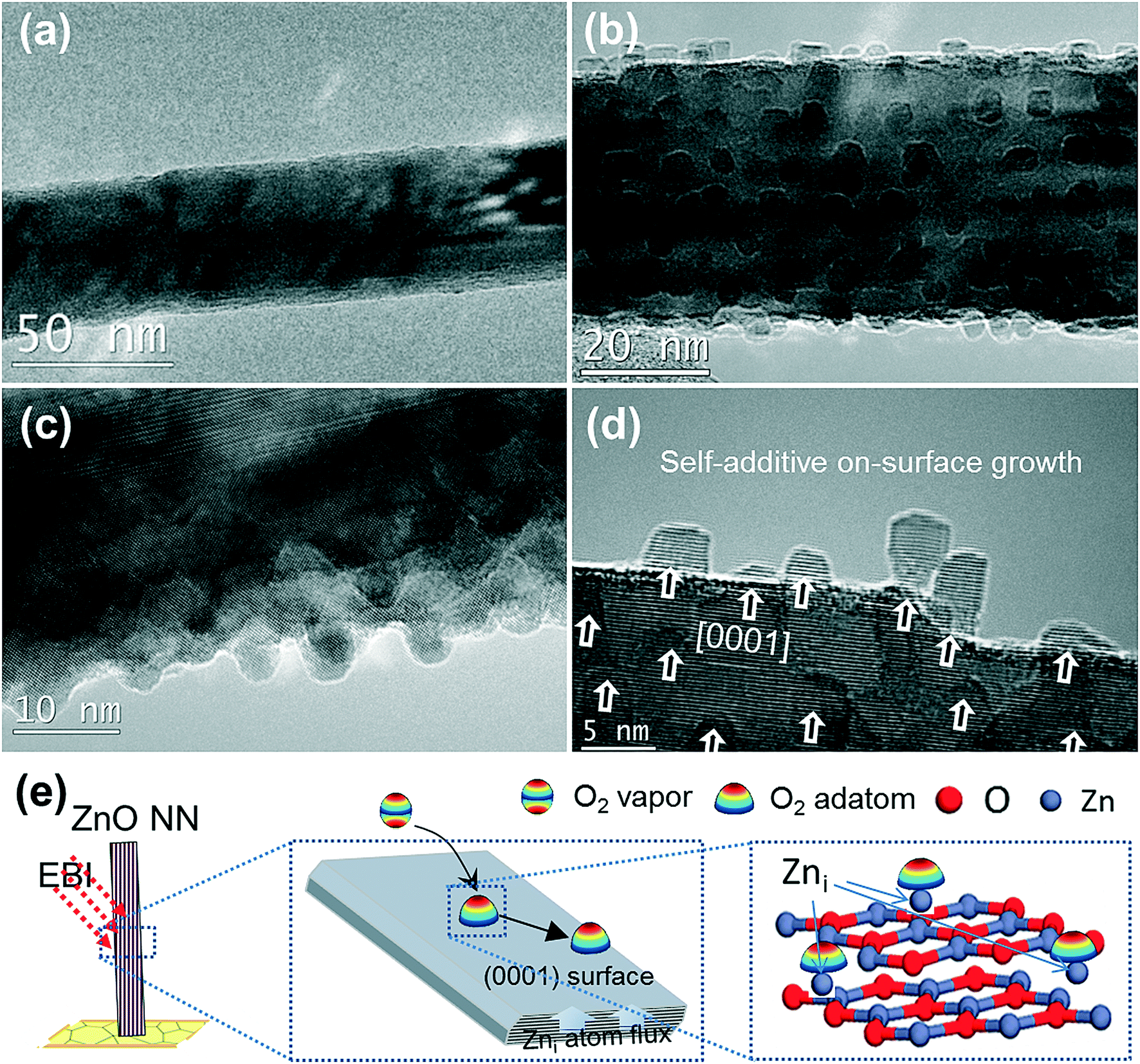 | ||
| Fig. 4 (a) Initial HRTEM image of another individual ZnO NN. (b)–(d) HRTEM images of an individual ZnO NN subjected to EBI. The arrows are drawn to guide the eye. (e) The electron-beam stimulated “self-additive on-surface oxidation-limited growth” at RT with numerous ZnO NCs on (0001) facets of a SC ZnO NN into a monolithic ZnO NC-on-NN SC hybrid. The inset shows physisorbed O2 molecules on Zni on the ZnO (0001) surface. | ||
Combined with the microstructural characterization (including PXRD, Raman, PL and XPS analysis) of the ZnO NNs grown (Fig. 2), the ZnO NNs can be determined to be highly defective SC with a higher concentration or numerous Vo or Zni, which is probably due to the synthesis method. Namely, there is a higher concentration of excessive Zni exposed in ZnO NNs, serving as active sites for triggering the following reaction of ZnO nuclei as follows, Zni + O2 ⇒ ZnO. The total pressure at the specimen corresponds to the ‘6’ scale ∼ 1.18 × 10⁻⁵ Pa in the high-vacuum TEM, the partial pressure of O2 in the electron microscope column is estimated to be roughly 1.18 × 10⁻⁷ Pa.38 With this O2 partial pressure, the surrounding O2 vapors condense and are preferentially adsorbed onto a lower surface energy plane, i.e. the {0001} surface of the ZnO NNs, which is thermodynamically favorable. As a result, all arriving O2 molecules react with the Zn-rich ZnO (0001) surface of ZnO NNs. Previous results suggested that Zn-terminated ZnO (0001)-Zn polar faces are reactive for catalytic dehydrogenation and oxidation reactions.39 Numerous ZnO NCs form through absorbing surrounding O2 vapors, where defect or disorder is notably absent in the images (Fig. 3d and 4d). The direct on-site homoepitaxial growth of ZnO NCs directly from the Zni and physisorbed O2 molecules along the [0001] c-axis is related to an “interfacial assembly” on (0001) facets of SC [100] ZnO NNs. According to Van de Walle,40 Zni are shallow donors in n-type ZnO and are fast diffusers with migration barriers as low as 0.57 eV; they are therefore unlikely to be stable. During the EBI process, the electron energy is confined locally within ZnO NNs, and a single ZnO NN interacts strongly with the electron beam within the region (∼π (200 nm)2), absorbing a substantial amount of electron-beam energy estimated to be about 200 kV × (14800 e Å−2 s−1 × π (2000)2 Å2 × 240 s) ≈ 9 × 10¹⁸ eV, lowering the activation energy for self-diffusion of Zni, largely promoting outward migration of the small-diameter inner Zni along the spacious “Vo channels” to the surface of the ZnO NN (Fig. 3e). Although small, the Zn flux from the inside out is adequate. In contrast, the oxygen partial pressure is deficient in a TEM and the O2 near the Zni would be quickly consumed and depleted upon oxidation, the isolated ZnO NC continues to grow on the surface of the ZnO NN parent phases until the local oxygen partial pressure is completely exhausted. It is therefore proposed that the electron-beam stimulated “self-additive on-surface oxidation-limited growth” between oxygen partial pressure in electron microscopy and excessive Zni sites in the ZnO NN parent phases at RT (Fig. 4e).
Proceeding with the EBI process up to 25 minutes, the average diameter of ZnO NCs increases up to ∼6 nm (Fig. 5), exhibiting sluggish growth kinetics. Due to the isolation of “built-in” ZnO NCs on the ZnO NN in our case (Fig. 3d), the nucleation-and-growth of one ZnO NC is noninvasive during EBI, i.e. not growing into the other ZnO NC (Video S2†). Thus, due to EBI-assisted controlled oxidation of the Zni in electron microscopy, the unique reaction-limited on-site growth of ZnO NCs is responsible for the intrinsic stability (i.e., self-limiting growth) of the ZnO NCs. More significantly, it is in the quantum-confined size regime (diameter ≤7 nm for ZnO),41 thus tunable energy gaps and multiple exciton generation of ZnO QDs42,43 could be expected. Unfortunately; we lack the facility to quantitatively measure the optical properties of a single all-ZnO SC hybrid at nanoscale. Further work is under way on property measurement for such monolithic ZnO NC-on-NN SC hybrid arrays.
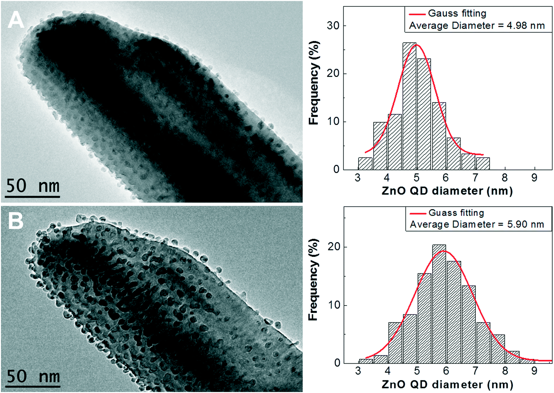 | ||
| Fig. 5 Self-limiting growth and thermal stability of ZnO NCs subjected to EBI. Comparative high-magnification TEM images of a single ZnO NN under FEB irradiation at different EBI times: (a) t = 15 min, and (b) t = 25 min. Right: the corresponding diameter distributions of ZnO NCs. | ||
In summary, our work experimentally proves that the EBI effect can be used for the effective integration of ultrahigh-density well-separated ZnO NCs homoepitaxially grown on the surface of an individual vertically oriented SC ZnO NN. The fabrication is made by a two-step zinc foil thermal oxidation and electron beam irradiation combination. To our knowledge, it is the first realization of ultrahigh-density ZnO NC on-site homoepitaxial growth on vertically oriented dense SC ZnO NNs from Zn foil substrate in this manner, which will encourage follow-up research. Detailed work is required to determine how electron energy and O2 vapor stimulated the ZnO NC growth in a gaseous environment (an environmental TEM); in particular, this question becomes essential when the EBI becomes a potential route to monolithic NC-on-NN SC hybrids. The vertically oriented growth of the monolithic ZnO 0-D NC-on-1-D NN SC hybrids is technologically important for engineered QD single-photon sources.44 Methodologically speaking, the microscopy-based “dry” electron-beam method provides a better solution with the advantages of fast-imaging and good positioning simultaneously.45 Due to its compatibility with the electron-beam lithography technique in chip fabrication where the programmable scanning electron-beam is focused on each nanowire at a time to get the NC array, the combination approach is amenable to the fabrication of nanodevices for industrial applications.
Acknowledgements
The author thanks Prof. R. Tenne for useful comments and J. Fang for experimental help. Supported by the National Science Foundation of Zhejiang Province (LY14E020005), and in part by the Fundamental Research Funds for the Central Universities of China (2014FZA3004).Notes and references
- S. Mann, Nat. Mater., 2009, 8, 781 CrossRef CAS PubMed.
- K. Miszta, et al. , Nat. Mater., 2011, 10, 872 CrossRef CAS PubMed.
- J. M. Li, Nanotechnology, 2010, 21, 175603 CrossRef PubMed.
- J. M. Li, X. L. Zeng, Q. Huang and Z. A. Xu, CrystEngComm, 2012, 14, 7800 RSC.
- J. M. Li, Cryst. Growth Des., 2009, 9, 4171 CAS.
- R. Elnathan, et al. , Nano Today, 2014, 9, 172 CrossRef CAS.
- X. Sun, Q. Li, J. C. Jiang and Y. B. Mao, Nanoscale, 2014, 6, 8769 RSC.
- A. Qurashi, J. H. Kim and Y. B. Hahn, Sol. Energy Mater. Sol. Cells, 2012, 98, 476 CrossRef.
- Z. L. Wang and J. H. Song, Science, 2006, 312, 242 CrossRef CAS PubMed.
- S. Wang, Z. L. Wang and Y. Yang, Adv. Mater., 2016, 28, 2881 CrossRef CAS PubMed.
- L. E. Brus, J. Chem. Phys., 1984, 80, 4403 CrossRef CAS.
- C. B. Murray, D. J. Norris and M. G. Bawendi, J. Am. Chem. Soc., 1993, 115, 8706 CrossRef CAS.
- S. S. Mali, H. J. Kim, P. S. Patil and C. K. Hong, Dalton Trans., 2013, 42, 16961 RSC.
- I. Robel, M. Kuno and P. V. Kamat, J. Am. Chem. Soc., 2007, 129, 4136 CrossRef CAS PubMed.
- R. Roy, M. Das and P. D. Dwivedi, Mol. Immunol., 2015, 63, 184 CrossRef CAS PubMed.
- B. O'Regan and M. Gratzel, Nature, 1991, 353, 737 CrossRef.
- G. H. Carey, A. L. Abdelhady, Z. J. Ning, S. M. Thon, O. M. Bakr and E. H. Sargent, Chem. Rev., 2015, 115, 12732 CrossRef CAS PubMed.
- R. Gao, Z. Q. Liang, J. J. Tian, Q. F. Zhang, L. D. Wang and G. Z. Cao, Nano Energy, 2013, 2, 40 CrossRef CAS.
- C. Florica, N. Preda, A. Costas, I. Zgura and I. Enculescu, Mater. Lett., 2016, 170, 156 CrossRef CAS.
- T. W. Kima, T. Kawazoea, S. Yamazakib, J. Limb, T. Yatsuia and M. Ohtsu, Solid State Commun., 2003, 127, 21 CrossRef.
- J. M. Li, L. G. Dai, X. P. Wan and X. L. Zeng, Appl. Phys. Lett., 2012, 101, 173105 CrossRef.
- J. M. Li, X. P. Wang, L. G. Dai and Z. A. Xu, CrystEngComm, 2013, 15, 1179 RSC.
- R. S. Wagner and W. C. Ellis, Appl. Phys. Lett., 1964, 4, 89 CrossRef CAS.
- J. Kim, J. Tersoff, S. Kodambaka, M. C. Reuter, E. A. Stach and F. M. Ross, Science, 2008, 322, 1070 CrossRef PubMed.
- V. Sahni, J. P. Perdew and J. Gruenebaum, Phys. Rev. B: Condens. Matter Mater. Phys., 1981, 23, 6512 CrossRef CAS.
- C. A. Arguello, D. L. Rousseau and S. P. S. Porto, Phys. Rev., 1969, 181, 1351 CrossRef CAS.
- J. M. Calleja and M. Cardona, Phys. Rev. B: Solid State, 1977, 16, 3753 CrossRef CAS.
- G. J. Exarhos and S. K. Sharma, Thin Solid Films, 1995, 270, 27 CrossRef CAS.
- A. Janotti and C. G. Van de Walle, Rep. Prog. Phys., 2009, 72, 126501 CrossRef.
- A. B. Djurisic and Y. H. Leung, Small, 2006, 2, 944 CrossRef CAS PubMed.
- S. Mahamuni, et al. , J. Appl. Phys., 1999, 85, 2861 CrossRef CAS.
- B. X. Lin, Z. Fu and Y. Jia, Appl. Phys. Lett., 2001, 79, 943 CrossRef CAS.
- V. G. Pol, R. Reisfeld and G. A. Gedanken, Chem. Mater., 2002, 14, 3920 CrossRef CAS.
- J. M. Li, X. L. Zeng, Y. H. Dong and Z. A. Xu, CrystEngComm, 2013, 15, 2372 RSC.
- In contrast, the Zn/ZnO interface along the basal plane {0001} is calculated to have a misfit of 21.6%.
- L. Vayssieres, Adv. Mater., 2003, 15, 464 CrossRef CAS.
- P. V. Radovanovic, N. S. Norberg, K. E. McNally and D. R. Gamelin, J. Am. Chem. Soc., 2002, 124, 15192 CrossRef CAS PubMed.
- For reference, the partial pressure of O2 in a vacuum is previously considered to be about two orders of magnitude smaller than the total pressure in JEM-2010.
- O. Dulub, U. Diebold and G. Kresse, Phys. Rev. Lett., 2003, 90, 016102 CrossRef PubMed.
- A. Janotti and C. G. Van de Walle, Phys. Rev. B: Condens. Matter Mater. Phys., 2007, 76, 165202 CrossRef.
- E. A. Meulenkamp, J. Phys. Chem. B, 1998, 102, 5566 CrossRef CAS.
- V. A. Fonoberov and A. A. Balandin, Appl. Phys. Lett., 2004, 85, 5971 CrossRef CAS.
- V. A. Fonoberov, K. A. Alim, A. A. Balandin, F. X. Xiu and J. L. Liu, Phys. Rev. B: Condens. Matter Mater. Phys., 2006, 73, 165317 CrossRef.
- S. Buckley, K. Rivoire and J. Vuckovic, Rep. Prog. Phys., 2012, 75, 126503 CrossRef PubMed.
- J. M. Li, Nanotechnology, 2004, 15, 551 CrossRef CAS.
Footnote |
| † Electronic supplementary information (ESI) available. See DOI: 10.1039/c6ce02187e |
| This journal is © The Royal Society of Chemistry 2017 |