
 Open Access Article
 This Open Access Article is licensed under a Creative Commons Attribution-Non Commercial 3.0 Unported Licence
Dielectrophoretic assembly of liquid-phase-exfoliated TiS3 nanoribbons for photodetecting applications†
R.
Frisenda
 *a,
E.
Giovanelli
a,
P.
Mishra
a,
P.
Gant
a,
E.
Flores
b,
C.
Sánchez
b,
J. R.
Ares
b,
D.
Perez de Lara
a,
I. J.
Ferrer
b,
E. M.
Pérez
*a and
A.
Castellanos-Gomez‡
*a
*a,
E.
Giovanelli
a,
P.
Mishra
a,
P.
Gant
a,
E.
Flores
b,
C.
Sánchez
b,
J. R.
Ares
b,
D.
Perez de Lara
a,
I. J.
Ferrer
b,
E. M.
Pérez
*a and
A.
Castellanos-Gomez‡
*a
aInstituto Madrileño de Estudios Avanzados en Nanociencia (IMDEA-Nanociencia), Campus de Cantoblanco, E-28049 Madrid, Spain. E-mail: riccardo.frisenda@imdea.org; emilio.perez@imdea.org; andres.castellanos@csic.es
bMaterials of Interest in Renewable Energies Group (MIRE Group), Dpto. de Física de Materiales, Universidad Autónoma de Madrid, 28049 Madrid, Spain
First published on 15th May 2017
Abstract
Liquid-phase exfoliation is a technique capable of producing large quantities of two-dimensional materials in suspension. Despite many efforts in the optimization of the exfoliation process itself, not much has been done towards the integration of liquid-phase-exfoliated materials in working solid-state devices. In this article, we use dielectrophoresis to direct the assembly of liquid-phase-exfoliated TiS3 nanoribbons between two gold electrodes to produce photodetectors working in the visible region. Through electrical and optical measurements we characterize the responsivity of the device and we find values as large as 3.8 mA W−1, which are more than one order of magnitude higher compared to state-of-the-art devices based on liquid-phase-exfoliated two-dimensional materials assembled by drop-casting or ink-jet methods.
Right after the first works on mechanically exfoliated two-dimensional (2D) materials,1–3 other preparation methods oriented toward their larger scale production have been rapidly explored and developed. A significant example of a bottom-up approach is chemical vapor deposition (CVD) that provides a way to synthesize high quantities of homogenous materials with large crystalline domains,4–6 but is costly and complicated. From the top-down perspective, liquid-phase exfoliation (LPE) is an appealing route to produce large amounts of 2D materials in the form of small crystallites suspended in a solvent.7–13 LPE represents a cheap technique that can be easily scaled up and has strong potential to be used in printed electronics.
Significant efforts have been made in the optimization of the LPE process,14–19 mostly aimed at controlling the thickness and lateral size of the flakes and increasing the concentration of the suspensions. However, the integration of LPE materials into functional devices still remains largely unexplored, with the exception of devices based on graphene inks.20,21 Additionally, Withers et al.22 showed that heterostructures could be assembled from liquid-phase-exfoliated 2D crystals and they designed a photodetector with a gate-tunable photoresponsivity of up to 43 μA W−1. In a different study, Yang et al.23 incorporated liquid-phase-exfoliated materials as dielectrics in graphene-based photodetectors. Zhu et al.24 reported similar findings on the outstanding dielectric properties of liquid inks made from thickness-sorted 2D hexagonal boron nitride.
Here, we demonstrate how titanium trisulfide (TiS3) nanoribbons obtained by LPE can be assembled between two metallic electrodes by dielectrophoresis (DEP) to fabricate photodetectors. TiS3 is a layered material that belongs to the family of semiconducting transition metal trichalcogenides and exhibits pronounced in-plane anisotropy25 and great potential to be used in optoelectronics.26–28 In the present paper we use DEP-assisted deposition to assemble liquid-phase-exfoliated TiS3 nanoribbons in between metallic electrodes to produce solid-state photodetectors. The device based on colloidal TiS3 shows improved responsivities as large as 3.8 mA W−1 compared to state-of-the-art LPE-based devices. The novel deposition method based on DEP, together with the excellent photodetecting properties of TiS3 retained in the liquid-phase-exfoliated material, paves the way for fabrication of novel and cheap photodetectors which can be easily scaled up for industrial applications.
Bulk TiS3 was prepared by surface sulfurization of bulk Ti powder at 500 °C, similarly to the procedure described in ref. 29. Fig. 1a shows a scanning electron microscopy (SEM) picture of lamellar bulk TiS3 and in the inset a photograph of the as-synthetized bulk TiS3 (Fig. S1, ESI†). We prepared TiS3 suspensions by ultrasonication of the bulk material in isopropyl alcohol (IPA). We employed successive centrifugation–redispersion sequences to sort out the suspensions according to TiS3 crystallite dimensions. Fig. 1b shows a photograph of four suspensions of TiS3 in IPA. From suspension A, resulting directly from the sonication step, three other suspensions labelled B, C and D were prepared. The centrifugation procedure led to the following order of decreasing particle weight in the suspension: B > C > D, whereas suspension A contains all possible particle dimensions. The different suspensions are stable from a few hours to several weeks and any of the suspensions can be easily redispersed by simple stirring, which enables long-term use of the colloids.
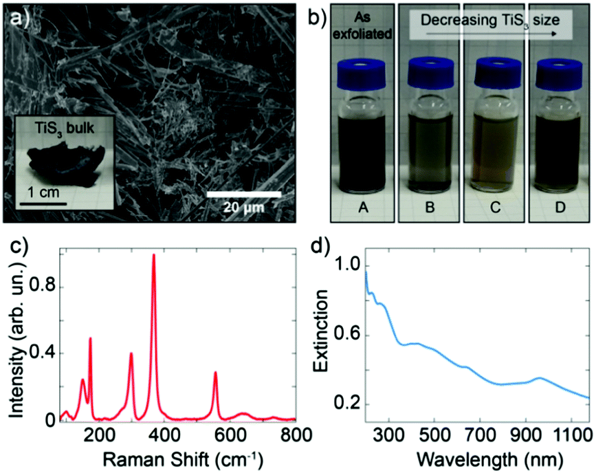 | ||
| Fig. 1 (a) SEM image of the lamellar TiS3 bulk material. Inset: Photograph of bulk TiS3. (b) Optical image of the colloidal suspensions of exfoliated TiS3 in IPA. (c) Raman spectrum (normalized at 368 cm−1) and (d) UV-Vis-NIR spectrum of colloidal suspension D. | ||
Fig. 1c shows the Raman spectrum of suspension D measured with an excitation wavelength of 532 nm and an optical power of 2 mW. Raman spectra of all four colloids present similar features (Fig. S2–S4, ESI†), indicating that LPE results in analogous structures. The Raman spectra are in agreement with those of the bulk30–33 and with those of mechanically exfoliated few-layer TiS3,34 with additional bands that indicate the presence of TiO2 in the form of the anatase polytype,35,36 probably due to surface/edge oxidation of TiS3. Raman analysis of the bulk confirms that TiO2 is found right from the beginning in the starting material, but further oxidation during the sonication process cannot be excluded.37
The optical properties of liquid-phase-exfoliated TiS3 were studied by UV–Vis–NIR spectroscopy (Fig. 1d and Fig. S5, ESI†). These absorption properties are in agreement with an optical bandgap of 1.07 eV (corresponding to an absorption onset of 1160 nm) reported for as synthesized bulk material.38 This is expected as the band structure of TiS3 is mostly thickness independent.38,39 The Tauc plot (Fig. S6, ESI†), which is generated from the absorption data of suspension D, confirms that the TiS3 nanoribbons have a direct optical bandgap of 1.02 eV, consistent with values from the literature.29,38,40
In order to integrate liquid-phase-exfoliated TiS3 into functional devices, we employed DEP-assisted deposition. In the DEP phenomenon, a non-uniform electric field polarizes the suspended particles of a colloid within the corresponding solvent and gradients in the electric field force the alignment of the particles (dipoles) with the local field lines and push these particles towards regions of most intense field. The relative polarizabilities of both components of the colloid (suspended particles and solvent) are crucial for this process. In previous studies, DEP has been used successfully as a method to assemble carbon nanotubes41 or graphene42–44 between metallic electrodes, but its use with other two-dimensional materials is rather scarce and very recent.28
In our implementation of the technique, sketched in Fig. 2a, a 1 MHz sinusoidal signal of 10 V peak-to-peak is applied between drain and source electrodes, which are separated by 5 μm. A drop of the TiS3 colloidal suspension is cast onto the electrodes and the electric field generated by the oscillating source–drain voltage polarizes the nanoribbons with respect to the solvent. The gradients in the electric fields push these nanoribbons toward the region of highest electric field intensity. TiS3 nanoribbons are thus deposited in a controlled way, preferentially bridging the electrodes, between which the electric field intensity is the highest. This allows the fabrication of a fully packed TiS3 channel out of a suspension of relatively low concentration. TiS3 LPE was performed in IPA due to its ability to efficiently stabilize the resulting colloidal nanoribbons, its relatively low boiling point, and its weak polarizability (≈7 Å3, see ref. 45). The DEP force acting on tube-shaped particles (which is a good approximation to the TiS3 nanoribbons) can be written as:
| FDEP ∝ εm Re[(εp* − εm*)/(εm*)]∇|E|2 |
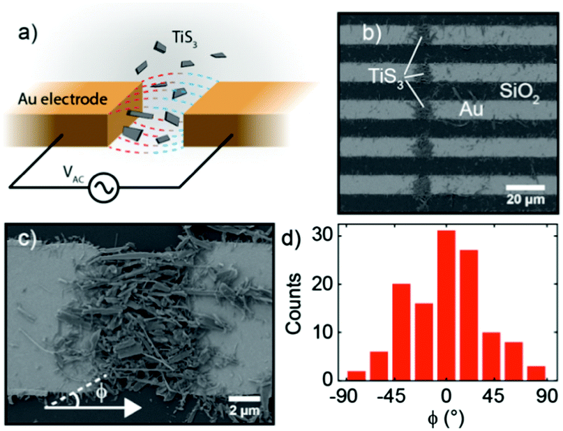 | ||
| Fig. 2 (a) Sketch of the DEP technique used to fabricate TiS3-based photodetecting devices from the liquid-phase-exfoliated material. (b and c) SEM images of aligned TiS3 nanoribbons between gold electrodes assembled from suspension D. (d) Angular distribution of the assembled TiS3 nanoribbons where 0° corresponds to a nanoribbon oriented along the source–drain electrode direction. The angle was measured from 123 nanoribbons identified in the SEM image of panel (c). | ||
From now on in the main text we will focus on the DEP-based assembly from suspension D, which contains the smallest particles. A SEM image of the resulting device is shown in Fig. 2b and c shows a zoom in the region separating one particular pair of electrodes. From these images, it can be seen that most of the TiS3 nanoribbons have accumulated in the region between the electrodes, where the source and drain electrodes face each other, with only a small amount of the material deposited on the side of the electrodes or on the SiO2 surface. Moreover, thanks to DEP-assisted deposition, TiS3 nanoribbons mostly adopt an orientation that is parallel to the source–drain direction, as confirmed by the analysis of the angular distribution of the nanoribbons in relation to the electrodes shown in Fig. 2d. The peak at 0° indicates that the preferred TiS3 configurations are those in which the nanoribbon length is parallel to the source–drain direction (Fig. S7, ESI†). A distribution of the nanoribbon lengths is shown in Fig. S8 of the ESI.†
After the DEP assembly, we characterized the electrical transport of the fabricated device at room temperature and under high-vacuum conditions (P ≈ 2 × 10⁻⁶ mbar). Fig. 3a shows the current–voltage (I–V) characteristics of the device recorded in the dark and under illumination with a blue laser (λ = 405 nm). The laser has been focused on the device surface in a spot size of approximately 120 μm diameter. Under dark conditions, the I–V characteristic is asymmetric in bias and the maximum current flowing through the device reaches approximately 25 μA at a bias voltage of 1 V. Upon illumination, the device shows an enhancement of the current because of the photogeneration of charge carriers, visible in the I–V curves of Fig. 3a recorded for increasing laser intensities. For samples with a large amount of loosely connected nanoribbons the electrical characteristics turned out not to be reproducible because of continuous switching that we attribute to the electromechanical motion of the nanoribbons. See for example a device built from suspension A (Fig. S9 and S10, ESI†) which shows frequent switches in current with and without illumination.
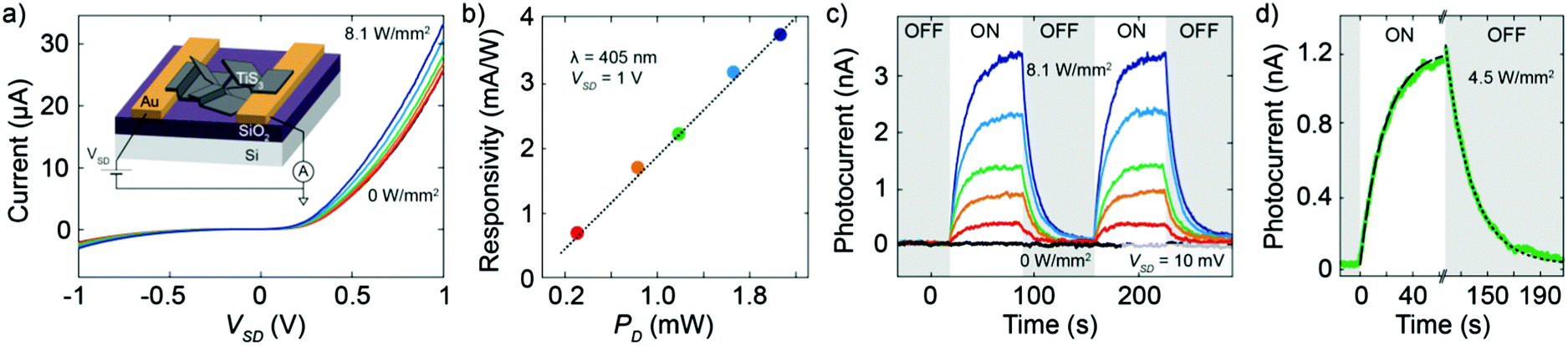 | ||
| Fig. 3 (a) Current–voltage characteristics of the LPE-based TiS3 device in the dark and upon illumination with a laser (wavelength 405 nm) for increasing light power densities up to 8.1 W mm−2. Inset: Schematic illustration of the fabricated device. (b) Responsivity at a bias voltage of 1 V as a function of light power. The dashed line is a linear fit to the data. (c) Time response of the photocurrent recorded at a bias voltage of 10 mV upon a modulated optical excitation (frequency 8 mHz) for increasing laser power densities up to 8.1 W mm−2. (d) Time response at an optical power density of 4.5 W mm−2. The dashed lines are fit to an exponential decay function; the time constant of the system is 8 ± 2 s. | ||
The generated photocurrent in the device made from suspension D reaches a value of 7.4 μA at 1 V with a light/dark current ratio of 1.3. Fig. 3b shows the responsivity of the device at a bias of 1 V as a function of the incident laser power PD. The responsivity at each laser power is calculated from the I–V curves by dividing the photocurrent at a voltage of 1 V by the product of the total incident illumination power density and the active area of the device. The largest responsivity is 3.8 mA W−1, recorded for the largest excitation power PD. The extracted responsivity is low when compared to that of a single TiS3 nanoribbon26 which is many orders of magnitude higher. This can be explained by the fact that in the present case the transport in the device is dominated by the TiS3/TiS3 interfaces and not by the intrinsic TiS3 material properties, giving lower overall performances, as was already observed18 in the case of LPE MoS2. Interestingly, the responsivity shows a pronounced linear dependence on the excitation power. This monotonous increase in responsivity for increasing incident power is relatively unusual in low-dimensional semiconducting photodetectors, for which a monotonous decrease as a function of power is usually observed. Such a linear increasing behavior has been explained theoretically in other semiconducting devices by the presence of recombination centers with different intragap energies in the semiconductor.18,46 The incident light shifts the Fermi level, thus changing the occupancy of these centers, which can result in a larger lifetime of the carriers at higher incident power densities. Due to the LPE method our devices are likely to contain various defects, which could account for the linear dependence of the responsivity on the excitation power.
Finally, in order to study the time response of the device we measured the source–drain current as a function of time while switching on and off the illumination. Fig. 3c shows the photocurrent recorded during several switching cycles at a bias voltage of 10 mV and with increasing illumination power. The response time extracted from Fig. 3d is τ = (8 ± 2) s. In addition, we studied the photoresponse with a laser of 638 nm in order to rule out a possible contribution to the photoresponse due to the presence of TiO2 given its negligible response for excitation wavelengths longer than 500 nm.47 The small variations in the responsivity at 638 nm and 405 nm (Fig. S11, ESI†) are in good agreement with the energy dependence of TiS3 nanoribbon absorptivity, excluding any significant contribution of TiO2 to the photoresponse of the device.
In conclusion, we have studied a solid-state photodetector based on liquid-phase-exfoliated TiS3 nanoribbons. We have shown that a dielectrophoresis-based deposition method can produce high-quality devices by assembling the TiS3 ink onto metallic electrodes. Electrical and optical measurements reveal that the responsivities and the general performances of our devices are better compared to state-of-the-art photodetectors based on liquid-phase-exfoliated materials.
We acknowledge funding from the European Commission (Graphene Flagship, CNECTICT-604391). A. C. G. acknowledges financial support from the MINECO (Ramón y Cajal 2014 RYC-2014-01406 and MAT2014-58399-JIN) and from the Comunidad de Madrid (MAD2D-CM Program (S2013/MIT-3007)). R. F. acknowledges support from NWO through the research program Rubicon with project number 680-50-1515. D. PdL. acknowledges the support from MICINN/MINECO (Spain) through the program FIS2015-67367-C2-1-P. E. M. P. acknowledges funding from the European Research Council MINT (ERC-StG-2012-307609), the MINECO of Spain (CTQ2014-60541-P) and the Comunidad de Madrid (MAD2D project, S2013/MIT-3007). E. G. acknowledges support from the AMAROUT II program (Marie Curie Action, FP7-PEOPLE-2011-COFUND (291803)). E. F., C. S., J. R. A. and I. J. Ferrer acknowledge support from MINECO through the project MAT2015-65203R.
Notes and references
- K. S. Novoselov, A. K. Geim, S. V. Morozov, D. Jiang, Y. Zhang, S. V. Dubonos, I. V. Grigorieva and A. A. Firsov, Science, 2004, 306, 666–669 CrossRef CAS PubMed.
- M. Yi and Z. Shen, J. Mater. Chem. A, 2015, 3, 11700–11715 CAS.
- A. Castellanos-Gomez, M. Buscema, R. Molenaar, V. Singh, L. Janssen, H. S. van der Zant and G. A. Steele, 2D Mater., 2014, 1, 011002 CrossRef.
- Y. H. Lee, X. Q. Zhang, W. Zhang, M. T. Chang, C. T. Lin, K. D. Chang, Y. C. Yu, J. T. W. Wang, C. S. Chang and L. J. Li, Adv. Mater., 2012, 24, 2320–2325 CrossRef CAS PubMed.
- Y. Zhan, Z. Liu, S. Najmaei, P. M. Ajayan and J. Lou, Small, 2012, 8, 966–971 CrossRef CAS PubMed.
- H. Schmidt, S. Wang, L. Chu, M. Toh, R. Kumar, W. Zhao, A. Castro Neto, J. Martin, S. Adam and B. Özyilmaz, Nano Lett., 2014, 14, 1909–1913 CrossRef CAS PubMed.
- Y. Hernandez, V. Nicolosi, M. Lotya, F. M. Blighe, Z. Sun, S. De, I. McGovern, B. Holland, M. Byrne and Y. K. Gun'Ko, Nat. Nanotechnol., 2008, 3, 563–568 CrossRef CAS PubMed.
- J. N. Coleman, Adv. Funct. Mater., 2009, 19, 3680–3695 CrossRef CAS.
- J. N. Coleman, M. Lotya, A. O'Neill, S. D. Bergin, P. J. King, U. Khan, K. Young, A. Gaucher, S. De and R. J. Smith, Science, 2011, 331, 568–571 CrossRef CAS PubMed.
- V. Nicolosi, M. Chhowalla, M. G. Kanatzidis, M. S. Strano and J. N. Coleman, Science, 2013, 340, 1226419 CrossRef.
- A. Ciesielski and P. Samorì, Chem. Soc. Rev., 2014, 43, 381–398 RSC.
- L. Niu, J. N. Coleman, H. Zhang, H. Shin, M. Chhowalla and Z. Zheng, Small, 2016, 12, 272–293 CrossRef CAS PubMed.
- D. Fadil, R. H. Fayaz and A. B. Kaul, MRS Adv., 2016, 1, 3223–3228 CrossRef CAS.
- A. B. Bourlinos, V. Georgakilas, R. Zboril, T. A. Steriotis and A. K. Stubos, Small, 2009, 5, 1841–1845 CrossRef CAS PubMed.
- G. S. Bang, K. W. Nam, J. Y. Kim, J. Shin, J. W. Choi and S.-Y. Choi, ACS Appl. Mater. Interfaces, 2014, 6, 7084–7089 CAS.
- P. Yasaei, B. Kumar, T. Foroozan, C. Wang, M. Asadi, D. Tuschel, J. E. Indacochea, R. F. Klie and A. Salehi-Khojin, Adv. Mater., 2015, 27, 1887–1892 CrossRef CAS PubMed.
- A. G. Kelly, T. Hallam, C. Backes, A. Harvey, A. S. Esmaeily, I. Godwin, J. Coelho, V. Nicolosi, J. Lauth, A. Kulkarni, S. Kinge, L. D. A. Siebbeles, G. S. Duesberg and J. N. Coleman, Science, 2017, 356, 69–73 CrossRef CAS PubMed.
- S. Ghosh, A. Winchester, B. Muchharla, M. Wasala, S. Feng, A. L. Elias, M. B. M. Krishna, T. Harada, C. Chin, K. Dani, S. Kar, M. Terrones and S. Talapatra, Sci. Rep., 2015, 5, 11272 CrossRef CAS PubMed.
- K. Lee, H.-Y. Kim, M. Lotya, J. N. Coleman, G.-T. Kim and G. S. Duesberg, Adv. Mater., 2011, 23, 4178–4182 CrossRef CAS PubMed.
- F. Torrisi, T. Hasan, W. Wu, Z. Sun, A. Lombardo, T. S. Kulmala, G.-W. Hsieh, S. Jung, F. Bonaccorso and P. J. Paul, ACS Nano, 2012, 6, 2992–3006 CrossRef CAS PubMed.
- D. L. Gonzalez Arellano, H. Lee, E. B. Secor, E. K. Burnett, M. C. Hersam, J. J. Watkins and A. L. Briseno, ACS Appl. Mater. Interfaces, 2016, 8, 29594–29599 CAS.
- F. Withers, H. Yang, L. Britnell, A. P. Rooney, E. Lewis, A. Felten, C. R. Woods, V. Sanchez Romaguera, T. Georgiou, A. Eckmann, Y. J. Kim, S. G. Yeates, S. J. Haigh, A. K. Geim, K. S. Novoselov and C. Casiraghi, Nano Lett., 2014, 14, 3987–3992 CrossRef CAS PubMed.
- H. Yang, F. Withers, E. Gebremedhn, E. Lewis, L. Britnell, A. Felten, V. Palermo, S. Haigh, D. Beljonne and C. Casiraghi, 2D Mater., 2014, 1, 011012 CrossRef.
- J. Zhu, J. Kang, J. Kang, D. Jariwala, J. D. Wood, J.-W. T. Seo, K.-S. Chen, T. J. Marks and M. C. Hersam, Nano Lett., 2015, 15, 7029–7036 CrossRef PubMed.
- J. O. Island, R. Biele, M. Barawi, J. M. Clamagirand, J. R. Ares, C. Sánchez, H. S. van der Zant, I. J. Ferrer, R. D'Agosta and A. Castellanos-Gomez, Sci. Rep., 2016, 6 CAS.
- J. O. Island, M. Buscema, M. Barawi, J. M. Clamagirand, J. R. Ares, C. Sánchez, I. J. Ferrer, G. A. Steele, H. S. van der Zant and A. Castellanos-Gomez, Adv. Opt. Mater., 2014, 2, 641–645 CrossRef CAS.
- J. O. Island, M. Barawi, R. Biele, A. Almazan, J. M. Clamagirand, J. R. Ares, C. Sanchez, H. S. van der Zant, J. V. Alvarez, R. D'Agosta, I. J. Ferrer and A. Castellanos-Gomez, Adv. Mater., 2015, 27, 2595–2601 CrossRef CAS PubMed.
- D. D. Deng, Z. Lin, A. L. Elías, N. Perea-Lopez, J. Li, C. Zhou, K. Zhang, S. Feng, H. Terrones and J. S. Mayer, ACS Nano, 2016, 10, 5006–5014 CrossRef CAS PubMed.
- I. J. Ferrer, M. D. Maciá, V. Carcelén, J. R. Ares and C. Sánchez, Energy Procedia, 2012, 22, 48–52 CrossRef CAS.
- S. P. Gwet, Y. Mathey and C. Sourisseau, Phys. Status Solidi B, 1984, 123, 503–517 CrossRef CAS.
- D. W. Bullett, in Theoretical aspects of band structures and electronic properties of pseudo-one-dimensional solids, ed. H. Kamimura and D. Reidel Publishing Company, Dordrecht, Holland, 1985, pp. 160–230 Search PubMed.
- P. Gard, F. Cruege, C. Sourisseau and O. Gorochov, J. Raman Spectrosc., 1986, 17, 283–288 CrossRef CAS.
- A. S. Pawbake, J. O. Island, E. Flores, J. R. Ares, C. Sanchez, I. J. Ferrer, S. R. Jadkar, H. S. J. van der Zant, A. Castellanos-Gomez and D. J. Late, ACS Appl. Mater. Interfaces, 2015, 7, 24185–24190 CAS.
- A. Lipatov, P. M. Wilson, M. Shekhirev, J. D. Teeter, R. Netusil and A. Sinitskii, Nanoscale, 2015, 7, 12291–12296 RSC.
- T. Ohsaka, F. Izumi and Y. Fujiki, J. Raman Spectrosc., 1978, 7, 321–324 CrossRef.
- L. Mahoney and R. Koodali, Materials, 2014, 7, 2697–2746 CrossRef.
- A. Jawaid, D. Nepal, K. Park, M. Jespersen, A. Qualley, P. Mirau, L. F. Drummy and R. A. Vaia, Chem. Mater., 2016, 28, 337–348 CrossRef CAS.
- A. J. Molina-Mendoza, M. Barawi, R. Biele, E. Flores, J. R. Ares, C. Sánchez, G. Rubio-Bollinger, N. Agraït, R. D'Agosta, I. J. Ferrer and A. Castellanos-Gomez, Adv. Electron. Mater., 2015, 1, 1500126 CrossRef.
- J. Dai and X. C. Zeng, Angew. Chem., Int. Ed., 2015, 54, 7572–7576 CrossRef CAS PubMed.
- J. O. Island, M. Barawi, R. Biele, A. Almazán, J. M. Clamagirand, J. R. Ares, C. Sánchez, H. S. J. van der Zant, J. V. Álvarez, R. D'Agosta, I. J. Ferrer and A. Castellanos-Gomez, Adv. Mater., 2015, 27, 2595–2601 CrossRef CAS PubMed.
- A. Vijayaraghavan, S. Blatt, D. Weissenberger, M. Oron-Carl, F. Hennrich, D. Gerthsen, H. Hahn and R. Krupke, Nano Lett., 2007, 7, 1556–1560 CrossRef CAS PubMed.
- C. D. Sire, F. Ardiaca, S. Lepilliet, J.-W. T. Seo, M. C. Hersam, G. Dambrine, H. Happy and V. Derycke, Nano Lett., 2012, 12, 1184–1188 CrossRef CAS PubMed.
- B. R. Burg, J. Schneider, S. Maurer, N. C. Schirmer and D. Poulikakos, J. Appl. Phys., 2010, 107, 034302 CrossRef.
- B. R. Burg, F. Lütolf, J. Schneider, N. C. Schirmer, T. Schwamb and D. Poulikakos, Appl. Phys. Lett., 2009, 94, 053110 CrossRef.
- R. Bosque and J. Sales, J. Chem. Inf. Comput. Sci., 2002, 42, 1154–1163 CrossRef CAS PubMed.
- V. Klee, E. Preciado, D. Barroso, A. E. Nguyen, C. Lee, K. J. Erickson, M. Triplett, B. Davis, I.-H. Lu and S. Bobek, Nano Lett., 2015, 15, 2612–2619 CrossRef CAS PubMed.
- A. Molina-Mendoza, A. Moya, R. Frisenda, S. A. Svatek, P. Gant, S. Gonzalez-Abad, E. Antolín, N. Agrait, G. R. Bollinger and D. P. de Lara, J. Mater. Chem. C, 2016, 4, 10707–10714 RSC.
Footnotes |
| † Electronic supplementary information (ESI) available. See DOI: 10.1039/c7cc01845b |
| ‡ Present address: Instituto de Ciencia de Materiales de Madrid (ICMM-CSIC), Campus de Cantoblanco, E-28049 Madrid, Spain. |
| This journal is © The Royal Society of Chemistry 2017 |