
 Open Access Article
 This Open Access Article is licensed under a
 Creative Commons Attribution 3.0 Unported Licence
Improved color stability of complementary WOLED with symmetrical doped phosphors in single host: experimental verification and mechanism analysis
Kexiang Wangac,
Zhixiang Gaob,
Yanqin Miao *ac,
Long Gaoac,
Bo Zhaoac,
Huixia Xuac,
Zhongqiang Wangac,
Hua Wangac and
Bingshe Xuac
*ac,
Long Gaoac,
Bo Zhaoac,
Huixia Xuac,
Zhongqiang Wangac,
Hua Wangac and
Bingshe Xuac
aKey Laboratory of Interface Science and Engineering in Advanced Materials of Ministry of Education, Taiyuan University of Technology, Taiyuan, 030024, PR China. E-mail: miaoyanqin@tyut.edu.cn; Fax: +86-351-6010311; Tel: +86-351-6014852
bSchool of Physical Science and Electronics, Shanxi Datong University, Datong, 037009, PR China
cResearch Center of Advanced Materials Science and Technology, Taiyuan University of Technology, Taiyuan, 030024, PR China
First published on 5th July 2017
Abstract
In this work, by symmetrically doping blue and orange phosphors in a single host, a complementary all-phosphor white organic light-emitting diode (WOLED) was demonstrated. Compared with the reference white device with blue-orange sequential cascade dopants in a single host, the proposed WOLED with (blue-orange-blue) symmetrical arranged dopants shows an improved spectra stability with a change in Commission Internationale de L'Eclairage (CIE) coordinates of less than (±0.020, ±0.010) as the driving voltage increases from 4 V to 9 V, corresponding to the luminance increasing from 100 cd m−2 to about 15![[thin space (1/6-em)]](https://www.rsc.org/images/entities/char_2009.gif) 000 cd m−2. The improvement of color stability should be ascribed to the symmetric dopants in the multi-doped single host being able to effectively offset the spectral change caused by the shift of carrier recombination zone with the increase of driving voltage. This is confirmed by systematic probe devices, where the shift of carrier recombination zone was observed to give a more detailed analysis.
000 cd m−2. The improvement of color stability should be ascribed to the symmetric dopants in the multi-doped single host being able to effectively offset the spectral change caused by the shift of carrier recombination zone with the increase of driving voltage. This is confirmed by systematic probe devices, where the shift of carrier recombination zone was observed to give a more detailed analysis.
1 Introduction
White organic light-emitting diodes (WOLEDs) have drawn great attention for their potential applications in solid-state lighting and flat-panel display fields.1–6 Since both fluorescent and phosphorescent materials are used to fabricate WOLEDs, to date, various configurations have been proposed to improve the device performance.7,8 Among these approaches, all phosphor-doped WOLED technology was demonstrated to be the most effective method because phosphors can harvest both singlet and triplet excitons and realize a theoretical internal quantum efficiency of 100%.9–13 In terms of complexity and cost, the single-host structure, i.e., using a large-band gap host doped with two or more emissive dopants to generate white light, suggests its great potential for mass production and commercial reality in the future.14–16During the past decades, many efficient single-host WOLEDs have been developed, and the maximum external quantum efficiency (EQE) have reached the theoretical limit of 20%.17 However, the more stable spectra, which is a crucial parameter for the commercial applications of WOLEDs, still need to be further improved in single-host WOLEDs.18–20 For instance, Han et al.18 reported a single phosphine oxide host for high-efficiency complementary WOLED with extremely low operating voltage and reduced efficiency roll-off, but this white device showed large Commission Internationale de L'Eclairage (CIE) coordinates' variation with (0.45, 0.45) at 1482 cd m−2 shift to (0.42, 0.44) at about 10000 cd m−2. Wang et al.19 reported an efficient dual-emissive-layer WOLED with blue and yellow phosphors doped in a single host, the resulting white device showed a poor color stability with CIE coordinates' variation above (±0.09, ±0.04) from 4 V to 8 V. In short, the voltage-dependent color shifts exceeding a tolerable margin are generally observed in these devices with multi-emission layers structure in single host.
Until now, many reasons have been found to cause the poor color stability for single-host WOLEDs.21 Among these reasons, the shift of carrier recombination zone at different voltages is widely considered to be one of the main factors.22–24 Since the mobility of hole and electron in organic materials generally alters with the change of applied electric field in the devices, which usually causes the shift of carrier recombination zone, leading to a poor color stability for WOLEDs.25–27 Up to date, many efforts have been made to overcome this problem.28–31 For example, the interlayer is introduced between the adjacent emission layers to suppress the variation of color by limiting carriers or excitons in the individual emission zone.32 However, the introduction of the interlayer frequently suppresses the power efficiency and increases the complexity of mass production.33
In this paper, we successfully fabricated blue-orange complementary all-phosphor WOLED without interlayer by symmetrically doping two phosphors in single host (blue-orange-blue) and found that the spectra stability of the WOLED was greatly improved. Compared with the large CIE coordinates' variation nearly above (±0.050, ±0.010) of the reference white device with blue-orange sequential cascade dopants in single host, the proposed symmetrical doped white device shows a more stable electroluminescence (EL) spectra with CIE coordinates' variation less than (±0.020, ±0.010) at the same driving voltage range from 4 V to 9 V, corresponding to the luminance increases from 100 cd m−2 to about 15000 cd m−2. Systematic probe devices were fabricated to detect the main carrier recombination zone. Particularly, the shift of carrier recombination zone was observed to give a more detailed analysis. Furthermore, the resulting color stable WOLED also shows a maximum current efficiency (CE), power efficiency (PE) and EQE of 20.9 cd A−1, 16.8 lm W−1, and 12.2%, respectively.
2 Experimental
As shown in the top of Fig. 1, in this work, two types of white device were mainly investigated, which are the white device with sequential cascade dopants in single host and the white device with symmetrical arranged dopants in single host, named as W1 and W2, respectively. Detailed device structures were shown in follows: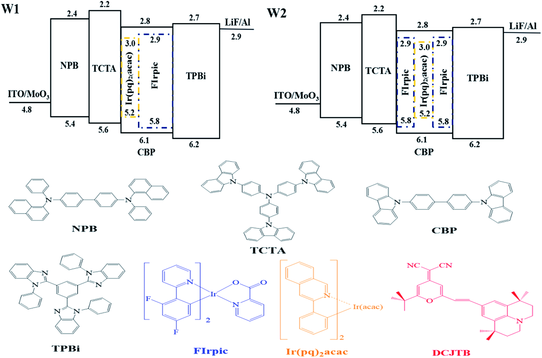 | ||
| Fig. 1 Top: Energy level diagrams and device configurations of W1 and W2. Bottom: molecular structure of the organic materials used in this paper. | ||
Device W1: ITO/MoO3 (3 nm)/NPB (30 nm)/TCTA (10 nm)/CBP:Ir(pq)2acac 8 wt% (10 nm)/CBP:FIrpic 20 wt% (20 nm)/TPBi (35 nm)/LiF (1 nm)/Al (100 nm).
Device W2: ITO/MoO3 (3 nm)/NPB (30 nm)/TCTA (10 nm)/CBP:FIrpic 20 wt% (10 nm)/CBP:Ir(pq)2acac 8 wt% (10 nm)/CBP:FIrpic 20 wt% (10 nm)/TPBi (35 nm)/LiF (1 nm)/Al (100 nm).
In these devices, N,N-bis(naphthalen-1-yl)-N,N-bis(phenyl)-benzidine (NPB), 4,4′,4′′-tri(9-carbazoyl)triphenylamine (TCTA) and 1,3,5-tri(1-phenyl-1H-benzo[d]imidazol-2-yl)-phenyl (TPBi) were used as the hole transporting layer (HTL), electron blocking layer (EBL) and electron transport layer (ETL), respectively; 4,4′-bis(carbazol-9-yl)biphenyl (CBP) was used as a common ambipolar host; bis(4,6-difluorophenyl-pyridine)(picolinate)iridium(III) (Firpic) and bis(2-phenylquinolinato)-acetylacetonate iridium(III) (Ir(pq)2acac) were selected as blue, orange phosphorescent emitters, respectively. Molybdenum trioxide (MoO3) and lithium fluoride (LiF) were used as hole inject layer (HIL) and electron inject layer (EIL), respectively. The molecular structure of the organic materials used in this paper were shown in the bottom. All materials used for device fabrication were obtained through commercial sources and used without further purification.
All the devices were fabricated on the pre-patterned indium tin oxide (ITO) glass substrate with sheet resistance of 10 Ω □−1. ITO substrates were scrubbed and sonicated consecutively with detergent water, deionized water, and acetone, dried in drying cabinet, and then exposed to a UV-ozone environment for 10 min. After these processes, the substrates were transferred into a vacuum chamber for sequential deposition of all organic functional layers by thermal evaporation below a vacuum of 5 × 10⁻⁴ Pa. The deposition rates for organic materials, MoO3, LiF, and aluminum (Al) were about 1, 0.3, 0.1 and 5 Å s−1, respectively. The thickness and deposition rates of the films were controlled by a quartz thickness monitor. The overlap between ITO anode and Al cathode is 3 mm × 3 mm, as the active emissive area of the devices.
The current density–voltage–luminance (J–V–L) characteristics of devices were measured by a computer-controlled BM-7A luminance meter and a Keithley 2400 programmable voltage current source. EL spectra and CIE coordinates of devices were measured by a computer-controlled PR655 Spectra scan spectrometer. The organic films for photoluminescence (PL) test were deposited on the quartz substrate in the same way as the devices, and the PL spectra of the films were investigated by a Fluoromax-4 luminescence spectrometer. The UV-Vis absorption spectrum was recorded by a U-3900 spectrophotometer. All the measurements were carried out directly after fabrication without encapsulation in ambient atmosphere at room temperature.
3 Results and discussion
Generally, due to the alteration of carrier recombination zone, multi-doped single-host WOLEDs without interlayer show unavoidable spectral variation at different driving voltages.19 This was further confirmed in our work.Fig. 2 depicts the normalized EL spectra of the reference device W1 at different driving voltages. Clearly, two intense emission peaks at 470 nm and 600 nm were observed, which were assigned to the emissions from FIrpic and Ir(pq)2acac, respectively. In addition, it can be seen that the relative intensity of blue emission decreases obviously as the driving voltage increases from 4 V to 9 V (corresponding to luminance increases from 100 cd m−2 to about 15000 cd m−2), especially at high driving voltages, i.e., 8 V and 9 V, leading to a poor color stability. Meanwhile, the CIE coordinates of device W1 shift from (0.424, 0.365) to (0.473, 0.376), showing large variation of above (±0.050, ±0.010). The drastically weakened blue emission should be attributed to less exciton recombination and blue emission in FIrpic-doped area with the increase of driving voltage, which may be caused by the change of main carrier recombination zone in device W1. Detailed reasons were given in the next discussion.
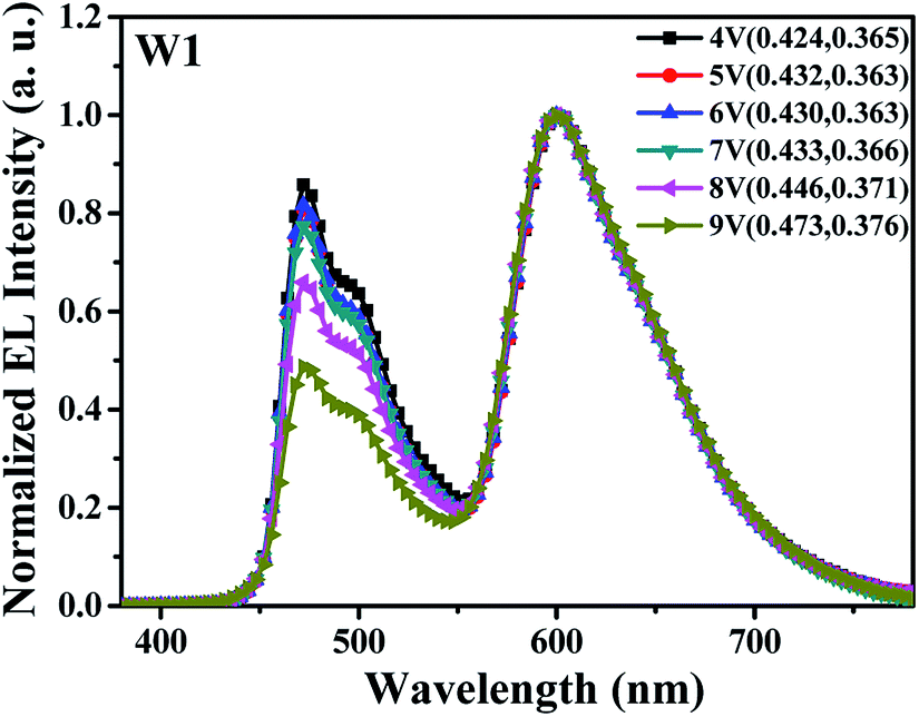 | ||
| Fig. 2 The normalized EL spectra of device W1 at different driving voltages. | ||
In order to explore the main carrier recombination zone and further prove the shift of carrier recombination zone in device W1, by incorporating an ultra-thin 4-(dicyanomethylene)-2-tert-butyl-6-(1,1,7,7-tetramethyljulolidin-4-yl-vinyl)-4H-pyran (DCJTB) layer in the different positions of blue emitting layer (EML), a series of probe devices were fabricated. Detailed structures for probe devices are as follows: ITO/MoO3 (3 nm)/NPB (30 nm)/TCTA (10 nm)/CBP:FIrpic 20 wt% (30 − x nm)/DCJTB (0.5 nm)/CBP:FIrpic 20 wt% (x nm)/TPBi (35 nm)/LiF (1 nm)/Al (100 nm), where x was set as 0 nm, 5 nm, 10 nm, 15 nm, 20 nm, 25 nm, 30 nm, respectively. DCJTB is a typical red fluorescent emitter, possessing high fluorescent quantum yield.34 Here, it was used as a probe with it's emission intensity in EL spectra represents the exciton density of different positions. Fig. 3 shows the normalized EL spectra of all probe devices at a voltage of 7 V, and the inset is the simplified structure diagram for probe devices. It can be seen that the EL spectra for all probe devices contain two emission peaks located at 470 nm and about 630 nm, which are typically derived from the emissions of FIrpic and DCJTB, respectively. Obviously, the probe device with x = 0 nm, corresponding to an ultra-thin DCJTB layer located at CBP/TPBi interface, shows the strongest intensity of red emission. And with the increases of x from 0, 5, 10, 15, 20, 25, to 30 along with the ultra-thin DCJTB layer away from CBP/TPBi interface, the corresponding probe devices exhibit gradually reduced the relative intensity of red emission. This phenomenon proves the main carrier recombination zone is located at the CBP/TPBi interface at 7 V. And the exciton density decreases with the increase of the distance to CBP/TPBi interface. In addition, with the increase of x, the EL spectra for corresponding probe devices display a blue-shift red emission peak. This is because that the emission wavelength for DCJTB is closely related to its doping concentration, which has been widely confirmed.35 Here, the spectral shift of DCJTB should be attributed to the different magnitudes of exciton density in different positions of EML where the ultra-thin DCJTB layer was inserted.
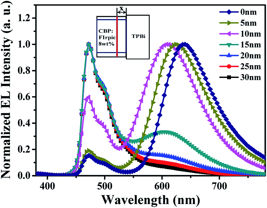 | ||
| Fig. 3 The normalized EL spectra of all probe devices measured at 7 V, and inset is the simple structure diagram of probe devices. | ||
Fig. 4 represents the normalized EL spectra of the probe devices (x = 0 nm, 10 nm, 20 nm, 30 nm) at different voltages from 4 V to 9 V, and the inset is the amplifying EL spectra of red wavelength at different driving voltages. From Fig. 4(a) and (b) (devices with x = 0 nm and 10 nm, where the ultra-thin DCJTB layer is close to the side of cathode in EML), clearly, the emission wavelength of red light from DCJTB shows a slightly blue shift along with the enhancement of blue emission intensity with the increase of driving voltages. The change of EL spectra clearly indicates the shift of carrier recombination zone. That is, the main carrier recombination zone is located at CBP/TPBi interface and the surrounding area near the CBP/TPBi interface in EML, and will slightly move to the direction of anode because electron mobility increases faster than hole mobility with the increase of applied voltage due to the different electric field-dependent mobility for organic materials used in these devices, leading to a decreased exciton density at CBP/TPBi interface and the surrounding area in EML under high driving voltages. With the ultra-thin DCJTB layer arranged in the EML close to the TCTA/CBP interface, corresponding to the devices with x = 20 nm and 30 nm, as shown in Fig. 4(c) and (d), both spectra show dominant blue emission. However, it is interesting that with the applied voltage increases, the intensity of red emission decreases at first and then rise. It can be explained as follows: DCJTB molecule usually shows a strong ability to capture carriers followed by direct exciton formation and emit red emission, especially at low voltages.36 And with the voltage increases, the red emission based on this mechanism will be weakened, resulting in a decreased intensity of red emission. But, the enhancement of red emission at high voltages, i.e., 8 V and 9 V, implies more excitons be used by DCJTB molecules, which is a direct evidence to prove the shift of carrier recombination zone at high driving voltages.
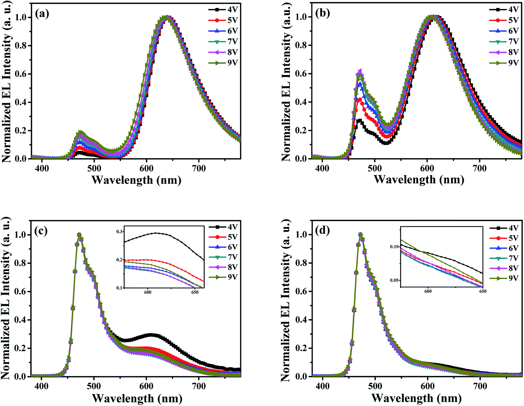 | ||
| Fig. 4 The normalized EL spectra of probe devices measured at different voltages, (a) x = 0 nm; (b) x = 10 nm; (c) x = 20 nm; (d) x = 30 nm. Inset: the amplifying EL spectra of red wavelength at different driving voltages. | ||
On the basis of the above discussion, a more detailed explanation can be given about the poor color stability for device W1. That is, the carrier recombination zone of W1 will slightly shift to anode with the increase of driving voltage, especially at high voltages, which will inevitably lead to a reduction of exciton that be used in the FIrpic-doped zone. In order to overcome this problem and further improve the spectra stability, the white device W2 without additional interlayer was successfully fabricated by symmetrically doping the blue and orange phosphorescent dopants in single host. The normalized EL spectra of device W2 at different driving voltages was shown in Fig. 5(a). Compared with the device W1, the spectra stability of device W2 is greatly improved, with CIE coordinates' variation less than (0.020, 0.010) as the driving voltage increases from 4 V to 9 V, which corresponds to the luminance increases from 100 cd m−2 to about 15000 cd m−2. Notably, within the luminance range of lighting or backlight applications, this WOLED exhibits a negligible CIE coordinates' variation of (±0.003, ±0.000) from 1000 cd m−2 to 5000 cd m−2. The enhanced spectra stability is mainly attributed to symmetrical doped blue phosphorescent dopants in single host that can effectively compensate for the loss of blue light caused by the shift of carrier recombination zone, thus inducing almost constant intensity of blue light.
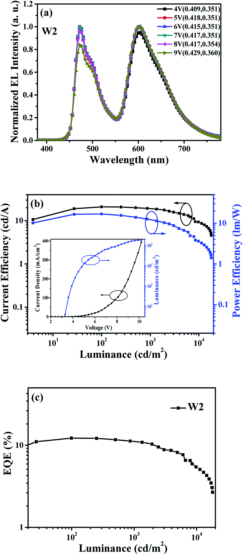 | ||
| Fig. 5 (a) The normalized EL spectra of device W2 at different driving voltages; (b) CE-L-PE characteristic for device W2, inset: J–V–L characteristic for device W2; (c) EQE-L characteristic for device W2. | ||
Fig. 5(b) and (c) show the CE-luminance-PE (CE-L-PE) characteristic and EQE-luminance (EQE-L) characteristic of device W2, and the inset of Fig. 5(b) is J–V–L characteristic. It can be seen that the device W2 shows the maximum CE, PE and EQE of 20.9 cd A−1, 16.8 lm W−1 and 12.2%, respectively. All the device efficiency tested in this work were only recorded in the forward direction and without the use of outcoupling technology. Here, it should be demonstrated that the efficiency of device W2 is relatively low, which may be caused by CBP is not an ideal host for FIrpic for its low triplet energy level (T1), and the more efficient white device may be anticipated by selecting suitable ambipolar hosts with higher T1.
In doped OLEDs, host–guest energy transfer and direct charge trapping followed by an exciton formation on guest are two main emission mechanisms.16,37 In order to clarify the emission mechanism of proposed white device, firstly, the absorption spectra of FIrpic and Ir(pq)2acac, and PL spectra of CBP were investigated.
As shown in Fig. 6, a large spectra overlap between the PL spectra of CBP and the absorption bands of FIrpic and Ir(pq)2acac were observed, indicating that the host–guests energy transfer process from CBP to FIrpic and Ir(pq)2acac can effectively happen in device W2.38 In addition, from the PL spectra of CBP:FIrpic (20 wt%) film and CBP:Ir(pq)2acac (8 wt%) film, it can be seen that the emission from CBP is completely quenched by FIrpic and Ir(pq)2acac, suggesting an efficient energy transfer from host to the dopants under such optimized doping concentrations. Therefore, there should exist the host–guests energy transfer process for blue and orange emissions in device W2. Besides, incomplete energy transfer from FIrpic molecules to Ir(pq)2acac molecules is inevitable since the former has a higher triplet energy than the latter, and there is no interlayer between them.29
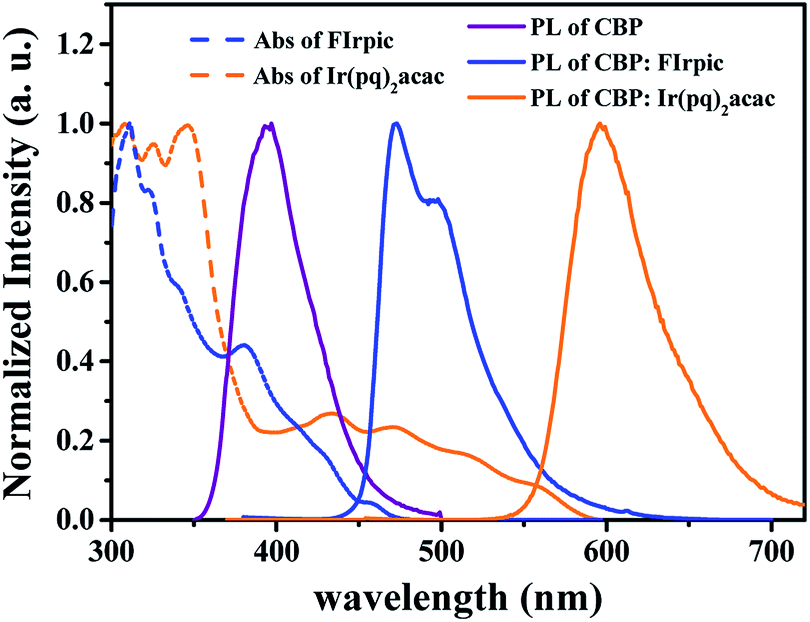 | ||
| Fig. 6 The normalized absorption spectra of FIrpic and Ir(pq)2acac (dissolved in tetrahydrofuran solvent) and the normalized PL spectra of CBP, CBP:FIrpic (20 wt%) and CBP:Ir(pq)2acac (8 wt%) (in thin solid films). | ||
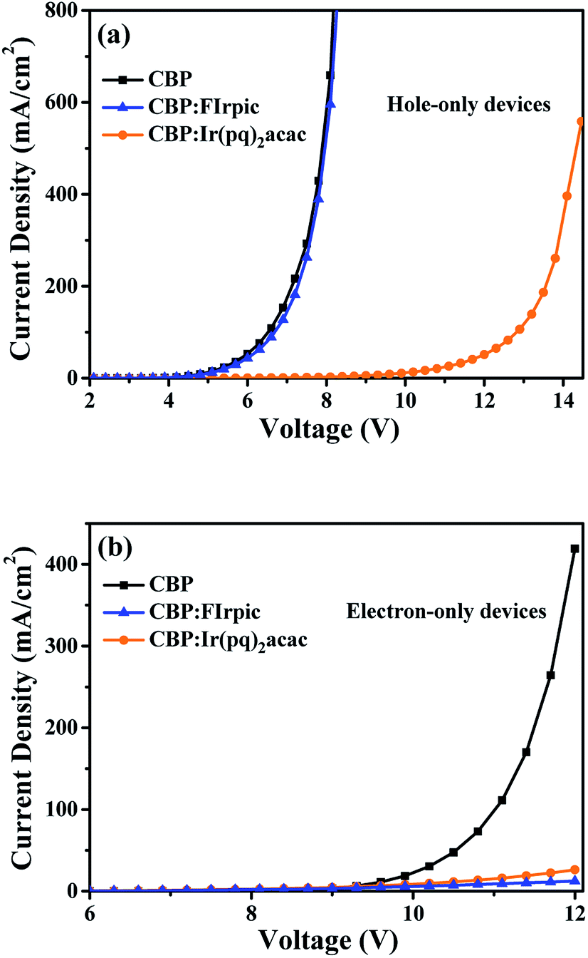
Further, a series of single carrier devices were fabricated to examine the possibility of trapping mechanism in the blue and orange emitters. Detailed device structures are shown in follows:
The hole-only devices: ITO/MoO3 (3 nm)/TCTA (10 nm)/CBP or CBP:FIrpic (20 wt%) or CBP:Ir(pq)2acac (8 wt%) (40 nm)/TCTA (10 nm)/Al (100 nm).
The electron-only devices: ITO/TPBi (10 nm)/CBP or CBP:FIrpic (20 wt%) or CBP:Ir(pq)2acac (8 wt%) (40 nm)/TPBi (10 nm)/LiF (1 nm)/Al (100 nm).
Fig. 7(a) and (b) depict the J–V characteristics of the single carrier devices, where we can see that the doped FIrpic molecules have a negligible impact on hole transport, but FIrpic molecules can effectively trap electrons, meaning that the direct carrier trapping should exist in the emission process of blue light. Meanwhile, it can be seen that the doped Ir(pq)2acac molecules can trap holes and electrons simultaneously, demonstrating the direct carrier trapping also exists in the emission process of orange light.39 Synthetically, as discussed above, the emission processes of blue and orange dopants should include both energy transfer and direct carrier trapping.
 | ||
| Fig. 7 (a) J–V characteristics of hole-only devices; (b) J–V characteristics of electron-only devices. | ||
Actually, the charge trapping was reported to have a deteriorated effect on the color stability of WOLEDs.38,40 The reason are as follows: in multi-doped WOLEDs, if the direct charge trapping dominates the emission of emitters, especially for red emitting materials with narrow energy gap, the spectra of corresponding WOLED is unstable since the narrow-energy gap emitters can efficiently capture charges and emit at low voltages, thus inducing a relative high emission intensity. As the driving voltage increases, more carriers will be injected, and the trapped sites will be filled followed by declined relative emission intensity. However, in our color stable WOLED, though the effect of charge trapping exists, the main emission mechanisms of two emitters are host–guest energy transfer which the majority of excitons generated on CBP and then transferred to blue/orange emitters. Thus, in this work, the charge trapping has a negligible effect on the color stability. The resulting color stable WOLED can be obtained via symmetrical arranged dopants in single host as the above mentioned, which can efficiently offset the spectra shift caused by the shift of carrier recombination zone. This novel design concept further proves the significant potential of symmetric dopants in enhancing the color stability of single-host WOLEDs.
4 Conclusions
In this work, by symmetrically doping the blue and orange phosphorescent dopants in single host, the spectra stability of a blue-orange complementary all-phosphor WOLED was developed successfully. The proposed white device exhibits extremely improved color stability with CIE coordinates' variation less than (±0.020, ±0.010) at the driving voltage range from 4 V to 9 V, corresponding to the luminance increases from 100 cd m−2 to about 15000 cd m−2. It is demonstrated that, with the increase of driving voltage, symmetrical dopants in multi-doped single host can effectively offsets the spectral change caused by the shift of carrier recombination zone. Our work may provide a simple method for realizing high color stability WOLEDs.
Acknowledgements
This work was supported by K. C. Wong Education Foundation – Hong Kong Baptist University (HKBU) Fellowship Programme for Mainland Visiting Scholars 2017–2018 Program for New Century Excellent Talents in University of Ministry of Education of China (NCET-13-0927); Shanxi Provincial Key Innovative Research Team in Science and Technology (No. 201605D131045-10); Natural Science Foundation for Shanxi Province (No. 201601D021018, 201601D011031), Shanxi University Scientific and Technical Innovation Project (No. 2016135).References
- B. W. D'Andrade and S. R. Forrest, Adv. Mater., 2004, 16, 1585 CrossRef.
- Y. Sun, N. C. Giebink, H. Kanno, B. Ma, M. E. Thompson and S. R. Forrest, Nature, 2006, 440, 908 CrossRef CAS PubMed.
- K. T. Kamtekar, A. P. Monkman and M. R. Bryce, Adv. Mater., 2010, 22, 572 CrossRef CAS PubMed.
- H. B. Wu, J. H. Zou, F. Liu, L. Wang, A. Mikhailovsky, G. C. Bazan, W. Yang and Y. Cao, Adv. Mater., 2008, 20, 696 CrossRef CAS.
- H. Wu, G. Zhou, J. Zou, C. L. Ho, W. Y. Wong, W. Yang, J. Peng and Y. Cao, Adv. Mater., 2009, 21, 4181 CrossRef CAS.
- G. Zhou, Q. Wang, C. L. Ho, W. Y. Wong, D. Ma and L. Wang, Chem. Commun., 2009, 24, 3574 RSC.
- Z. Wu and D. Ma, Mater. Sci. Eng., R, 2016, 107, 1 CrossRef.
- G. Zhou, W. Y. Wong and S. Suo, J. Photochem. Photobiol., C, 2010, 11, 133 CrossRef CAS.
- R. Wang, D. Liu, H. Ren, T. Zhang, H. Yin, G. Liu and J. Li, Adv. Mater., 2011, 23, 2823 CrossRef CAS PubMed.
- Y. S. Park, J. W. Kang, D. M. Kang, J. W. Park, Y. H. Kim, S. K. Kwon and J. J. Kim, Adv. Mater., 2008, 20, 1957 CrossRef CAS.
- Z. Zhang, P. Yan, S. Yue, Y. Chen, Q. Wu, D. Qu, R. Guo, P. Wang, Y. Zhao and S. Liu, Org. Electron., 2013, 14, 2172 CrossRef CAS.
- S. Gong, N. Sun, J. Luo, C. Zhong, D. Ma, J. Qin and C. Yang, Adv. Funct. Mater., 2014, 24, 5710 CrossRef CAS.
- Y. Sun and S. R. Forrest, Appl. Phys. Lett., 2007, 91, 263503 CrossRef.
- Q. Wang, J. Ding, D. Ma, Y. Cheng, L. Wang and F. Wang, Adv. Mater., 2009, 21, 2397 CrossRef CAS.
- Y. L. Chang, Y. Song, Z. Wang, M. G. Helander, J. Qiu, L. Chai, Z. Liu, G. D. Scholes and Z. Lu, Adv. Funct. Mater., 2013, 23, 705 CrossRef CAS.
- Q. Wang, J. Ding, D. Ma, Y. Cheng, L. Wang, X. Jing and F. Wang, Adv. Funct. Mater., 2009, 19, 84 CrossRef CAS.
- T. Fleetham, J. Ecton, Z. Wang, N. Bakken and J. Li, Adv. Mater., 2013, 25, 2573 CrossRef CAS PubMed.
- C. Han, G. Xie, H. Xu, Z. Zhang, L. Xie, Y. Zhao, S. Liu and W. Huang, Adv. Mater., 2011, 23, 2491 CrossRef CAS PubMed.
- Q. Wang, D. Ma, J. Ding, L. Wang, Q. Qiao, H. Jia, B. E. Gnade and J. Hoshikawa-Halbert, Org. Electron., 2015, 19, 157 CrossRef CAS.
- N. Sun, Q. Wang, Y. Zhao, D. Yang, F. Zhao, J. Chen and D. Ma, J. Mater. Chem. C, 2014, 2, 7494 RSC.
- S. Chen, Q. Wu, M. Kong, X. Zhao, Z. Yu, P. Jia and W. Huang, J. Mater. Chem. C, 2013, 1, 3508 RSC.
- S. S. Lee, D. Ko, C. H. Chung and S. M. Cho, Synth. Met., 2002, 128, 51 CrossRef CAS.
- U. S. Bhansali, H. Jia, M. A. Q. Lopez, B. E. Gnade, W. H. Chen and M. A. Omary, Appl. Phys. Lett., 2009, 94, 151 CrossRef.
- D. Berner, F. Nuesch, E. Tutiš, C. Ma, X. Wang, B. Zhang and L. Zuppiroli, J. Appl. Phys., 2004, 95, 3749 CrossRef CAS.
- C. H. Hsiao, S. W. Liu, C. T. Chen and J. H. Lee, Org. Electron., 2010, 11, 1500 CrossRef CAS.
- Y. S. Park, J. W. Kang, D. M. Kang, J. W. Park, S. K. Kwon, S. C. Shin and J. J. Kim, Adv. Mater., 2008, 20, 1957 CrossRef CAS.
- K. H. Kim, Y. S. Seo and D. G. Moon, Synth. Met., 2014, 189, 157 CrossRef CAS.
- L. Y. Guo, X. L. Zhang, M. J. Zhuo, C. Liu, W. Y. Chen, B. X. Mi, J. Song, Y. H. Li and Z. Q. Gao, Org. Electron., 2014, 15, 2964 CrossRef CAS.
- Y. Miao, Z. Gao, H. Wang, H. Jia, X. Liu and B. Xu, Org. Electron., 2015, 23, 199 CrossRef CAS.
- X. L. Li, G. Xie, M. Liu, D. Chen, X. Cai, J. Peng, Y. Cao and S. J. Su, Adv. Mater., 2016, 28, 4614 CrossRef CAS PubMed.
- Y. Miao, Z. Gao, Y. Li, A. Zhang, H. Wang, Y. Hao, H. Jia, X. Liu and B. Xu, Synth. Met., 2015, 203, 59 CrossRef CAS.
- F. Zhao, Z. Zhang, Y. Liu, Y. Dai, J. Chen and D. Ma, Org. Electron., 2012, 13, 1049 CrossRef CAS.
- N. Sun, Q. Wang, Y. Zhao, Y. Chen, D. Yang, F. Zhao, J. Chen and D. Ma, Adv. Mater., 2014, 26, 1617 CrossRef CAS PubMed.
- S. Tao, L. Niu, J. Yu, Y. Jiang and X. Zhang, J. Lumin., 2010, 130, 70 CrossRef CAS.
- F. J. Zhang, Z. Xu, D. W. Zhao, S. L. Zhao, L. W. Wang and G. C. Yuan, Phys. Scr., 2008, 77, 055403 CrossRef.
- Y. M. Wang, F. Teng, Z. Xu, Y. B. Hou, S. Y. Yang and X. R. Xu, Mater. Chem. Phys., 2005, 92, 291 CrossRef CAS.
- X. Yang, G. Zhou and W. Y. Wong, Chem. Soc. Rev., 2015, 44, 8484 RSC.
- L. Zhu, J. Chen and D. Ma, J. Appl. Phys., 2015, 118, 175503 CrossRef.
- L. Zhu, Z. Wu, J. Chen and D. Ma, J. Mater. Chem. C, 2015, 3, 3304 RSC.
- S. H. Kim, S. Park, J. E. Kwon and S. Y. Park, Adv. Funct. Mater., 2015, 21, 644 CrossRef.
| This journal is © The Royal Society of Chemistry 2017 |