
 Open Access Article
 This Open Access Article is licensed under a
 Creative Commons Attribution 3.0 Unported Licence
V–VO2 core–shell structure for potential thermal switching†
Keshab Dahal a,
Qian Zhangab,
Yumei Wangac,
Ishwar Kumar Mishraa and
Zhifeng Ren*a
a,
Qian Zhangab,
Yumei Wangac,
Ishwar Kumar Mishraa and
Zhifeng Ren*a
aDepartment of Physics and TcSUH, University of Houston, Houston, Texas 77204, USA. E-mail: zren@uh.edu
bDepartment of Materials Science and Engineering, Harbin Institute of Technology (Shenzhen), Shenzhen, Guangdong 518055, P. R. China
cBeijing National Laboratory for Condensed Matter Physics, Institute of Physics, Chinese Academy of Sciences, Beijing 100190, P. R. China
First published on 5th July 2017
Abstract
Since the cold start of the internal combustion engine is not fuel efficient for vehicles, a warm start is desired. In this work, we propose to use thermal switching materials to warm-up the engine quickly at the cold start. We found that the V–VO2 core–shell structure can be a thermal switching material, which yields a higher electrical conductivity due to the electron transfer from V to VO2 above the insulator to metal transition temperature. The surface of V particles was converted into VO2 by controlled annealing in air, resulting in a V–VO2 core–shell structure. With such a V–VO2 core–shell structure, electrical conductivity increased from 2.1 × 10⁵ to 5.1 × 10⁵ S m−1 through the insulator-to-metal transition, resulting in an electronic thermal conductivity increase from 1.51 to 4.87 W m−1 K−1.
Introduction
The internal combustion (IC) engine converts chemical energy in fuel to mechanical energy. The average fuel conversion efficiency of an IC engine is in the range of 35–40%,1 when the engine is completely warmed up with the lubricant temperature at 100–110 °C.2,3 However, it is only about 9% at the beginning when the engine is cold (with the lubricant below 25 °C).3,4 Therefore, knowledge of how to get the engine warmed up to its optimum temperature very quickly, is extremely important to the overall fuel efficiency of especially personal cars, since vehicles need about 5 to 10 minutes to warm up to their optimal efficiency.3 A warming up time of 5–10 min for each cold start is a very significant portion of the total driving time for personal cars. Ideally, the engine will warm up to the optimal temperature in the shortest time, if the thermal loss is zero below that temperature, but very high above that temperature to keep the engine at the optimal temperature for the best efficiency. This requires materials with thermal conductivity very low, to prevent heat from leaking out, below a certain temperature and very high above that temperature, to dissipate the heat when the engine is warmed up, preventing the engine from overheating. Such a function can only be achieved by a thermal switch: off/on, meaning a significant thermal conductivity change from very low to very high at the required temperature. Unfortunately such a thermal switch within the required temperature range does not exist. Our study mainly aims at demonstrating such a concept in a material structure.It is well known that thermal energy in solid is transported by two components: lattice (κL) and charges5 (κe = LoσT, where Lo = 2.44 × 10⁻⁸ W Ω K−2 is the Lorenz number, σ the electrical conductivity, and T the absolute temperature).6 In order to have a significant change, a phase change is necessary since two different structures will have different κL and κe. With increase in κe, we can expect increase in κ, if κL does not change too much.
In previous studies, some of the materials on their solid–liquid phase transition showed high switching capability, for example, Zn3Sb2,7 Cd0.999SbAg0.001,8 CdSb,8,9 AlSb,10–12 InSb13 etc., undergoes semiconductor to metal transition on melting, with κhigh/κlow ratio of 15.4, 8.25, 4.95, 5.05, 3.76, respectively. However, due to their higher melting temperature, these materials are not suitable for our proposed application in IC engines. Additionally, (C2H4)n14 and NbO2 (ref. 15–18) undergo solid–solid phase transition at 395 and 1080 K. For NbO2 thermal conductivity increases above transition temperature with κhigh/κlow ratio is only 1.02, and thermal conductivity decreases above transition temperature for (C2H4)n. Recently, different strategies have been used to demonstrate thermal switching,19–23 including in homogeneously mass-loaded carbon and boron nitride nanotubes,19 bulk material made of two oxides with different thermal conductivities,22 graphite/hexadecane suspension,24 van der Waals interface effect on boron nano ribbons,25 and electrochemical change on LiCoO2,26 however either thermal conductivity decreases at higher temperature or if increases, the values of κhigh/κlow is less than 2. Furthermore, the thermal conductivity ratio (κhigh/κlow) of 2–5 have been observed by electrochemically tuning the intercalated amount of lithium (Li) in the van der Waals gaps in the bulk MoS2.27
Vanadium dioxide VO2 has recently been studied for its insulator(solid)–metal(solid) phase transition at 68 °C, from monoclinic (insulating) to tetragonal rutile (metallic) crystal structure in bulk materials,28–33 thin films34–40 and nanocrystals.41–45 The associated electrical conductivity increases from 102 S m−1 at room temperature to 103–105 S m−1 at 120 °C.28–46 Accordingly, thermal conductivity increase is expected34,35 due to the increase in κe.
The best reported values of the thermal conductivity of the VO2 thin film34 and polycrystalline31 samples are shown in Fig. S1a in the ESI.† It is clear that even though the electrical conductivity changes by a factor of ∼10 in polycrystalline and more than 100 in film (Fig. S1b in the ESI†), the thermal conductivity only changes by a factor of less than 2, either increases in thin film34,35 or decreases in polycrystalline.31 The reason is that the absolute electrical conductivity of both materials above the insulator–metal transition is not high enough to result in a high κe, so the total κ is not high in metallic phase. It is clear only when the electrical conductivity is high enough, then change in κe can lead to a high total thermal conductivity. Since the total thermal conductivity of VO2 in the insulating state is of 3.5–4.5 W m−1 K−1, according to Wiedemann–Franz (W–F) relationship,6 we need to have electrical conductivity higher than 6 × 10⁶ S m−1 in the metallic state to result in electronic thermal conductivity of about 10 times higher. We know that the electrical conductivity of VO2 cannot satisfy this requirement, so we have to look for new ideas to get the required high electrical conductivity.
Core–shell structure has been proved as a noble way to improve the material properties including electrochemical catalytic performances,47–50 photocatalytic performances,51,52 as well as electrical properties.51,53–56 Such core–shell structure has been reported in the form of nanoparticle,47–50 nano rod,51,52 and nanowire.53–56 In this paper, we report our studies on a V–VO2 core–shell structure (Fig. 1(a)), hoping for the free electrons transferring from V to VO2 above the phase transition temperature to reach the electrical conductivity close to that of V: 5 × 10⁶ S m−1.57 Below the phase transition temperature, it is insulator, since all the electrons of V are confined in V by VO2 shell. However, above the phase transition temperature, VO2 becomes metallic and the free electrons of V can move into VO2 to make the bulk more conducting when VO2 is thin enough. For our V–VO2 core–shell system, it could be possible to achieve thermal conductivity increase by a factor of 5, if we can get dense sample so that in the metallic phase κ would be close to that of vanadium (∼30.7 W m−1 K−1)58 and in the insulating phase κ would be close to that of VO2 (3–6 W m−1 K−1) when each vanadium particles in sample enclosed completely by thin insulating VO2 layer. We're interested in this system because of its temperature driven solid-state thermal switching at temperature close to the optimum temperature of lubricant in the IC engine.
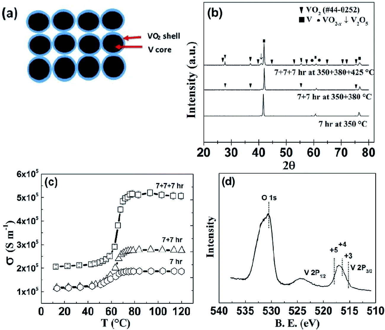 | ||
| Fig. 1 (a) Schematic of the V–VO2 core–shell structure, (b) XRD pattern of the step annealed V–VO2 powder samples, (c) electrical conductivity of core–shell V–VO2 bar samples annealed in air at different conditions as shown, and (d) XPS spectrum of 7 + 7 + 7 h sample, showing the chemical state of V. | ||
Previously, different methods have been used to prepare VO2 thin film. Some of the literatures have reported the preparation of VOx film first, and anneal it at different atmospheres (in air, O2, N2, Ar, etc.) in order to get or improve VO2 phase.59–62 The annealing temperature is different in different reports. Similarly, the preparation of VO2 films from V precursors have been reported in many papers.63–75 Annealing V resulted in different oxides depending on availability of oxygen through the depth, with V2O5 on the top, VO2 in the middle, and VO0.5–1.0 close to the substrate of the film.69–73 Such variation in oxidation state of V was controlled either by supplying low pressure oxygen or by making very thin V film to make the oxygen availability similar throughout the thickness of the film.75
In our case, the V–VO2 core–shell structure was formed by making the compacted pellet first and then converted the surface of each V particle into VO2 by controlled annealing in air. The formation of VO2 was confirmed by different measurements such as DSC heat flow curve and electrical resistivity. The XRD characterization and TEM analysis further confirmed it. The electrical and thermal conductivity near the phase transition temperature was also studied to support the concept.
Experimental
The V–VO2 core–shell structure was developed by a three step annealing of the pressed pellets in air. The V metal powder (99.5%, Alfa Aesar) with particle size <44 micron was cold pressed at ∼460 MPa pressure for 3 minutes to make porous disks. The disks were then cut into bars of 1.5 mm × 1.5 mm × 11 mm, and finally the bars were annealed in air in a tube furnace. The annealing was done at 350, 380, and 425 °C for 7 hour at each temperature, with a heating rate of 2 K min−1. For the XRD analysis, V powder was annealed. The phase formation was studied by XRD (X'Pert PRO PANalytical) with Cu-Kα radiation at room temperature and transmission electron microscope (TEM JEOL 2100F). The microstructure of the polished surface of the sample was studied by a scanning electron microscope (SEM, JEOL 6304F). The electrical as well as thermal conductivity of the samples were measured in the same direction by a four probe method using the thermal transport option (TTO) of a physical properties measurement system (PPMS, D060, Quantum Design) from room temperature to 120 °C. The latent heat of the sample was measured by the differential scanning calorimetry (DSC, 404 C, Netzsch). The errors for electrical conductivity and thermal conductivity are 3% and 5%, respectively.Results and discussion
The formation of V–VO2 core–shell structure (Fig. 1(a)) by oxidizing the surface of V particles is shown in the XRD patterns (Fig. 1(b)). The electrical conductivity of the samples prepared at different conditions is shown in Fig. 1(c). As shown, the sample annealed at 350 °C for 7 h clearly shows the transition in electrical conductivity across the phase transition of VO2. This transition at 68 °C indicates the initiation of formation of VO2, but very thin, since there is no visible peaks of VO2 on XRD pattern of powder sample, annealed in the same condition (Fig. 1(b)). Another sample was annealed at 350 °C for 7 hours plus 380 °C for 7 hour, and it was found that the transition in conductivity is sharper. Upon further annealing, a third sample annealed at 350 °C for 7 hours, then 380 °C for 7 hours, and then 425 °C for 7 hour, shows a much sharper change in electrical conductivity (Fig. 1(c)) by a factor of 2.5, as well as clear appearance of the peaks of VO2 in the XRD pattern (Fig. 1(b)). In comparing the XRD peak intensity, we noticed that the VO2 is still thin, but V2O5 started to form indicated by the arrow, which led us to not anneal the samples at even higher temperature. X-ray photoelectron spectroscopy (XPS) analysis (Fig. 1(d)) also shows that the sample annealed at 350 °C for 7 h + 380 °C for 7 h + 425 °C for 7 h (named as “7 + 7 + 7 h”) contains VO2 as well as V2O5. As we know the 2P3/2 peak of V3+, V4+, and V5+ lies at 515.29 eV,76 516.35 eV,77 and 517.91 eV (ref. 77) respectively. For our 7 + 7 + 7 h annealed sample, VO2 is present as major phase, with trace amount of other oxides of vanadium with oxidation states from +3 to +5 as impurity phase. As the sample annealed at 350 + 380 + 425 °C has the highest electrical conductivity above the transition, we chose this annealing condition for further study. With increase in annealing temperature and time, the sample is also denser, that's probably why the electrical conductivity in the insulating phase is also increased.HRTEM analysis of the V–VO2 core–shell samples is shown in Fig. 2. The high magnification image (Fig. 2(b)) taken at the edge of the sample (Fig. 2(a)) shows the lattice spacing of 0.206 nm, corresponding to the (120) plane of VO2.
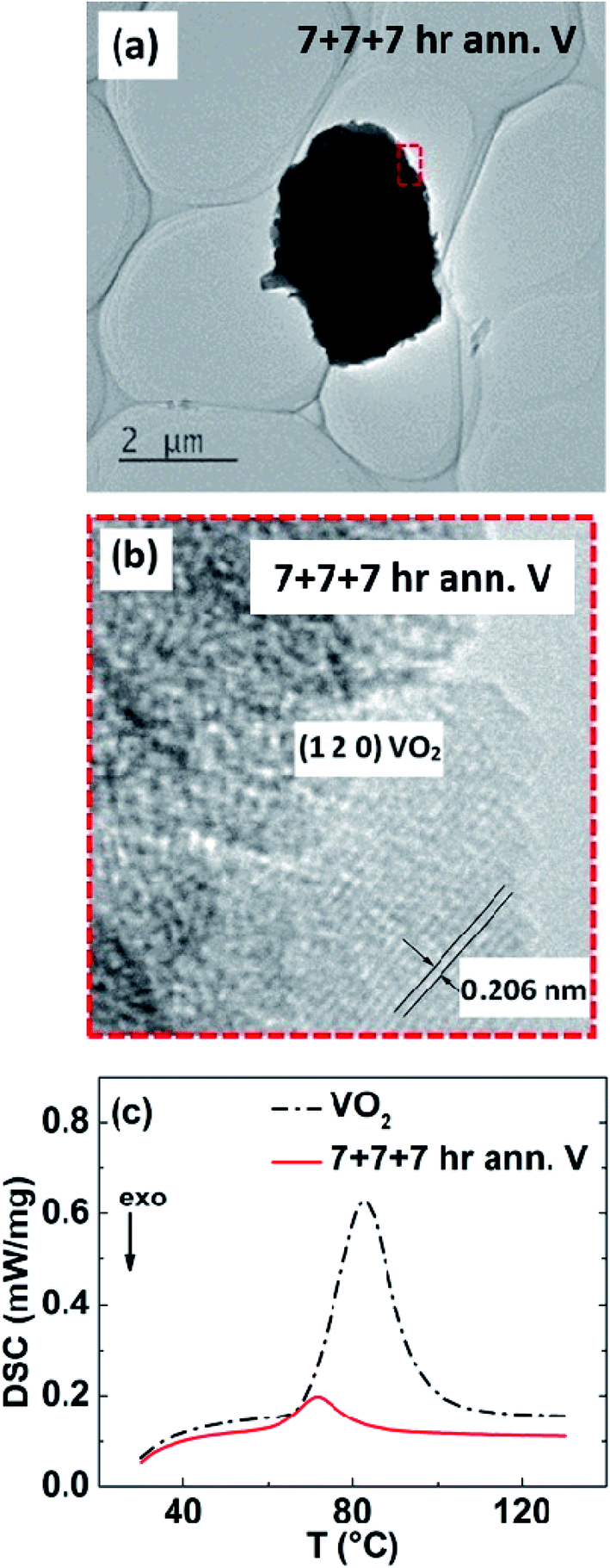 | ||
| Fig. 2 (a) Low magnification TEM image of 7 + 7 + 7 h sample, (b) HRTEM image of the edge of 7 + 7 + 7 h sample, and (c) specific heat absorption curve of the 7 + 7 + 7 h sample compared with that of VO2 bulk polycrystalline sample. | ||
The amount of VO2 formed on V is calculated by the latent heat measurement using DSC. Fig. 2(c) shows the heat absorption curve of the sample by DSC measurement. It is interesting to note that the peak of DSC curve for V–VO2 core–shell structured sample is shifted towards lower temperature due to the size effect.37,38,46 The latent heat for polycrystalline VO2 is found to be 43.37 J g−1 (which is a little bit lower than the reported value (51.65 ± 0.25) J g−1 for the single crystal30), but that of the V–VO2 core–shell sample is 4.97 J g−1, meaning only about 9–11% (mass) is VO2 and the rest about 90% is still V with trace amount of other vanadium oxides as impurity phase.
The thermal conductivity of the samples is shown in Fig. 3(a). It clearly shows a gradual thermal conductivity increase across the phase transition. For the 7 + 7 + 7 h annealed sample, thermal conductivity increased from 8.08 W m−1 K−1 at room temperature to 9.89 W m−1 K−1 at 120 °C, by about 22%. The room temperature total thermal conductivity increased with increasing temperature and time, which is probably due to better and better structure connection of the grains. Hall measurement shows that the carrier concentration increases across the transition (Fig. 3(d)), a clear demonstration of the core–shell modulation doping concept: electrons spill from V into VO2 above the transition. Since the carrier concentration of 7 + 7 + 7 h sample is higher than polycrystalline bulk VO2 sample33 (inset in Fig. 3(d)) before and after phase transition, which further confirms that the increase in electron density of 7 + 7 + 7 h sample above transition temperature is due to the electron spill from V into VO2. The Hall mobility (Fig. 3(e)) increases with temperature across the transition, which also supports the increase in electrical conductivity above the transition, different from most of the reports on VO2 (ref. 33, 36, 78 and 79) showing decrease in mobility. The small change in carrier density indicates that either in the metallic phase the electrons transferred from V to VO2 are not as many as we hope for, or the electrons blocked within V by VO2 in the insulating phase are not as many as we hoped for, or both, which is not understood right now. The electronic thermal conductivity (κe) (Fig. 3(b)) calculated by using W–F relationship, increased from 1.51 W m−1 K−1 at room temperature to 4.87 W m−1 K−1 at 120 °C for 7 + 7 + 7 h sample, with the lattice contribution decreased by 1.55 W m−1 K−1 (Fig. 3(c)). Previous reports29,31,33,80 also showed similar type of decrease in lattice thermal conductivity for sample with VO2 only, however, our sample has VO2 only 9–11% of the whole mass of the sample.
 | ||
| Fig. 3 (a) Thermal conductivity of V–VO2 core–shell samples, (b) electronic thermal conductivity of V–VO2 core–shell samples (empty symbol: using W–F law and filled symbol: effective value), (c) lattice thermal conductivity of V–VO2 core–shell samples (empty symbol: using W–F law and filled symbol: effective value), (d) carrier concentration of 7 + 7 + 7 h sample and inset shows the comparison of carrier concentration of polycrystalline bulk VO2 (ref. 33) with that of 7 + 7 + 7 h sample, (e) comparison of mobility of the 7 + 7 + 7 h sample with that of reported polycrystalline bulk as well as thin film VO2, and (f) effective Lorenz number of core–shell V–VO2 samples prepared at three different conditions. | ||
Even though the electrical conductivity of V could be close to 5 × 10⁶ S m−1 at room temperature,57 our V–VO2 core–shell samples only showed an electrical conductivity of about 5 × 10⁵ S m−1, an order of magnitude lower, which is most likely due to the low density of 5.28 g cm−3 for our V–VO2 core–shell sample (only about 90% of the theoretical density of 5.90 g cm−3). Such a low density will certainly results in low electrical conductivity due to the electron scattering in porous areas (SEM image in Fig. S3 in the ESI†). Another possible reason for the low electrical conductivity is the presence of V2O5 phase, since it has very low electrical conductivity (∼50 S m−1 at 120 °C).81 According to the XRD pattern of 7 + 7 + 7 h sample (after polishing its surface), there exist a trace amount of other oxides like VO2−x (VO0.5, etc.), which might also be responsible for the lowered electrical conductivity. For our sample, VO2−x phase couldn't be avoided completely, since there exist an oxygen gradient along the radial direction of each particle. We also found that the V2O5 phase is present only on the outer surface of each particle since XRD of the polished samples don't have V2O5 peak (Fig. S2 in the ESI†).
In principle, the intrinsic thermal conductivity of V–VO2 core–shell above the transition could be close to that of V (∼30 W m−1 K−1),58 but it is actually much lower (9.89 W m−1 K−1) due to the high porosity (low electrical conductivity), as shown in SEM image in Fig. S3 in the ESI,† as well as the presence of other vanadium oxides (XRD pattern in Fig. 1(b) and S2 in the ESI†). We now face a challenge how to oxidize the outer surface of each particle of a 100% dense pellet. Similarly, we were unable to avoid V2O5 phase on outer surface of each core–shell particle.
The electronic thermal conductivity of 7 + 7 + 7 h sample is increased by 3.36 W m−1 K−1; however, total thermal conductivity increased only by 1.81 W m−1 K−1, across the phase transition. Since, VO2 is only 10% (by mass) present in our sample, the lattice thermal conductivity across the transition shouldn't change by such a large amount (by ∼24% as in Fig. 3(c)), as previous reports shows ∼11% decrease in pure VO2 nano beam80 (calculated theoretically) and ∼27% decrease in VO2 polycrystalline samples29,31 (calculated using W–F relationship). Therefore, we can assume lattice thermal conductivity in the metallic phase (filled symbol in Fig. 3(c)), similar to that in the insulating phase. The effective electrical thermal conductivity (κeffe) in the metallic phase can be calculated by subtracting lattice thermal conductivity in the insulating phase from the total thermal conductivity in the metallic phase, as shown by filled symbol in Fig. 3(b). The effective Lorenz number in the metallic phase can be calculated by using  . The effective Lorenz number (Fig. 3(f)) of 7 h sample is found to be ∼0.85 Lo which is closer to Sommerfeld value (Lo); however, with increase in amount of VO2 on sample, the effective Lorenz number (Leff) decreased to 0.65 Lo for 7 + 7 h and 0.56 Lo for 7 + 7 + 7 h sample, which indicates the deviation of W–F law with increase in concentration of VO2 in the sample. Such a large deviation in W–F law with only 10% VO2 could be due to the fact that each V particle is surrounded by very thin VO2 layer and effect is significant. The decrease in value of effective Lorenz number with increased amount of VO2 is in agreement with the report by Lee et al.,80 as they have reported effective Lorenz number for pure VO2 nano-beam in the metallic phase equal to only ∼0.11 Lo. They also show the switching behavior of thermal conductivity on VO2 samples doped with the tungsten (W). This further indicates that, with only VO2 it is not possible to get increased total thermal conductivity by pursuing higher electrical conductivity. However, the core–shell concept is clearly demonstrated and can be applied to the W doped VO2 materials, which requires a significant amount of work and is out of the scope of this paper. Similarly, the material having phase transition temperature ∼100 °C is better for the application. Therefore, VO2 need to be modified to meet the requirement of phase transition temperature or need to search for new materials with phase transition temperature between 80 and 100 °C to get better performance.
Conclusion
We designed and studied a V–VO2 core–shell structure to realize a potential large change of thermal conductivity at the phase transition of VO2 due to transfer of the free electrons from V to VO2 above the transition temperature via modulation doping principle. The V–VO2 core–shell structure can potentially be used for thermal switching. The VO2 shell was formed by annealing V in air at limited temperatures to avoid formation of V2O5 and other higher oxides. We indeed observed higher electrical conductivity in V–VO2 core–shell samples than any of the reported polycrystalline bulk VO2 materials, but still about an order of magnitude lower than the expected value due to mainly low density (about 90%). Electronic thermal conductivity increased by 3.36 W m−1 K−1; however, total thermal conductivity increased by only 1.81 W m−1 K−1 across the phase transition, indicating the effective Lorenz number to be 0.56 Lo in the metallic phase. Even though the overall thermal conductivity increased only by 22%, it demonstrated the concept: increase thermal conductivity through increase of electronic thermal conductivity as a result of solid–solid phase transition.Acknowledgements
This work was supported by the US Department of Energy under a Contract DE-SC0010831 and Toyota Motors of North America.References
- J. B. Heywood, Internal Combustion Engine Fundamentals, McGraw-Hill, New York, 1988 Search PubMed.
- J. P. Zammit, P. J. Shayler and I. Pegg, presented in part at 10th Vehicle Thermal Management Systems Conference and Exhibition, Coventry, United Kingdom, 2010 Search PubMed.
- J. Trapy and P. Damiral, SAE [Tech. Pap.], 1990, 902089 CrossRef.
- F. Will and A. Boretti, SAE Int. J. Engines, 2011, 4, 175–187 CrossRef.
- C. A. Wert and R. M. Thomson, Physics of Solids, McGraw-Hill, New York, 1970 Search PubMed.
- R. Franz and G. Weidemann, Ann. Phys., 1853, 165, 497–531 CrossRef.
- A. Bath, J. G. Gasser and R. Kleim, Phys. Lett. A, 1982, 91, 355 CrossRef.
- S. Wang, J. Yang, L. Wu, P. Wei, J. Yang, W. Zhang and Y. Grin, Chem. Mater., 2015, 27, 1071 CrossRef CAS.
- S. Nakamura, T. Hibiya and F. Yamamoto, J. Appl. Phys., 1990, 68, 5125 CrossRef CAS.
- E. F. Steigmeier and I. Kudman, Phys. Rev., 1966, 141, 767 CrossRef CAS.
- W. Nakwaski, J. Appl. Phys., 1988, 64, 159 CrossRef CAS.
- N. F. Mott and A. S. Alexandrov, Sir Nevill Mott: 65 Years in Physics, World Scientific, Singapore, 1995 Search PubMed.
- V. I. Fedorov and V. I. Machuev, Fiz. Tekh. Poluprovodn., 1972, 6, 173 CAS.
- T. Zhang and T. Luo, ACS Nano, 2013, 7, 7592 CrossRef CAS PubMed.
- M. Kaviany, Heat Transfer Physics, Cambridge University Press, New York, 2014 Search PubMed.
- R. F. Janninck and D. H. Whitmore, J. Phys. Chem. Solids, 1966, 27, 1183 CrossRef CAS.
- A. O'Hara, T. N. Nunley, A. B. Posadas, S. Zollner and A. A. Demkov, J. Appl. Phys., 2014, 116, 213705 CrossRef.
- A. Y. Wu and R. J. Sladek, Phys. Rev. B: Condens. Matter Mater. Phys., 1982, 26, 2159 CrossRef CAS.
- C. W. Chang, D. Okawa, A. Majumdar and A. Zettl, Science, 2006, 314, 1121–1124 CrossRef CAS PubMed.
- H. Tian, D. Xie, Y. Yang, T.-L. Ren, G. Zhang, Y.-F. Wang, C.-J. Zhou, P. G. Peng, L.-G. Wang and L.-T. Liu, Sci. Rep., 2012, 2, 523 Search PubMed.
- G. Zhang and H. Zhang, Nanoscale, 2011, 3, 4604–4607 RSC.
- W. Kobayashi, Y. Teraoka and I. Terasaki, Appl. Phys. Lett., 2009, 95, 171905 CrossRef.
- D. Sawaki, W. Kobayashi, Y. Moritomo and I. Terasaki, Appl. Phys. Lett., 2011, 98, 081915 CrossRef.
- R. Zheng, J. Gao, J. Wang and G. Chen, Nat. Commun., 2011, 2, 289 CrossRef PubMed.
- J. Yang, Y. Yang, S. W. Waltermire, X. Wu, H. Zhang, T. Gutu, Y. Jiang, Y. Chen, A. A. Zinn, R. Prasher, T. T. Xu and D. Li, Nat. Nanotechnol., 2012, 7, 91–95 CrossRef CAS PubMed.
- J. Cho, M. D. Losego, H. G. Zhang, H. Kim, J. Zuo, I. Petrov, D. G. Cahil and P. V. Braun, Nat. Commun., 2013, 5, 4035 Search PubMed.
- G. Zhu, J. Liu, Q. Zheng, R. Zhang, D. Li, D. Banerjee and D. G. Cahill, Nat. Commun., 2016, 7, 13211 CrossRef CAS PubMed.
- F. J. Morin, Phys. Rev. Lett., 1959, 3, 34 CrossRef CAS.
- V. N. Andreev, F. A. Chudnovskii, A. V. Petrov and E. I. Terukov, Phys. Status Solidi A, 1978, 48, K153 CrossRef CAS.
- C. N. Berglund and H. J. Guggenheim, Phys. Rev., 1969, 185, 1022 CrossRef CAS.
- J. Chen, X. Liu, X. Yuan, Y. Zhang, Y. Gao, Y. Zhou, R. Liu, L. Chen and N. Chen, Chin. Sci. Bull., 2012, 57, 3393–3396 CrossRef CAS.
- M. Liu, A. J. Sternbach, M. Wagner, T. V. Slusar, T. Kong, S. L. Bud'ko, S. Kittiwatanakul, M. M. Qazilbash, A. Mcleod, Z. Fei, E. Abreu, J. Zhang, M. Goldflam, S. Dai, G. X. Ni, J. Lu, H. A. Bechtel, M. C. Martin, M. B. Raschke, R. D. Averitt, S. A. Wolf, H. T. Kim, P. C. Canfield and D. N. Basov, Phys. Rev. B: Condens. Matter Mater. Phys., 2015, 91, 245155 CrossRef.
- K. Dahal, Q. Zhang, R. He, I. K. Mishra and Z. Ren, J. Appl. Phys., 2017, 121, 155103 CrossRef.
- H. Kizuka, T. Yagi, J. Jia, Y. Yamashita, S. Nakamura, N. Taketoshi and Y. Shigesato, Jpn. J. Appl. Phys., 2015, 54, 053201 CrossRef.
- D.-W. Oh, C. Ko, S. Ramanathan and D. G. Cahill, Appl. Phys. Lett., 2010, 96, 151906 CrossRef.
- D. Ruzmetov, D. Heiman, B. B. Claflin, V. Narayanamurti and S. Ramanathan, Phys. Rev. B: Condens. Matter Mater. Phys., 2009, 79, 153107 CrossRef.
- L. Dai, C. Cao, Y. Gao and H. Luo, Sol. Energy Mater. Sol. Cells, 2011, 95, 712–715 CrossRef CAS.
- H. Liu, J. Lu, M. Zheng, S. H. Tang, C. H. Sow, X. Zhang and K. Lin, Opt. Express, 2014, 22, 30748 CrossRef CAS PubMed.
- J. Lu, K. G. West and S. A. Wolf, Appl. Phys. Lett., 2008, 93, 262107 CrossRef.
- K. G. West, J. Lu, J. Yu, D. Kirkwood, W. Chen, Y. Pei, J. Claassen and S. A. Wolf, J. Vac. Sci. Technol., A, 2008, 26, 133 CAS.
- J. Wu, Q. Gu, B. S. Guiton, N. P. de Leon, L. Ouyang and H. Park, Nano Lett., 2006, 6, 2313 CrossRef CAS PubMed.
- J. Cao, E. Ertekin, V. Srinivasan, W. Fan, S. Huang, H. Zheng, J. W. L. Yim, D. R. Khanal, D. F. Ogletree, J. C. Grossman and J. Wu, Nat. Nanotechnol., 2009, 4, 732–737 CrossRef CAS PubMed.
- A. Tselev, E. Strelcov, I. A. Luk'yanchuk, J. D. Budai, J. Z. Tischler, I. N. Ivanov, K. Jones, R. Proksch, S. V Kalinin and A. Kolmakov, Nano Lett., 2010, 10, 2003–2011 CrossRef CAS PubMed.
- T. J. Huffman, P. Xu, M. M. Qazilbash, E. J. Walter, H. Krakauer, J. Wei, D. H. Cobden, H. A. Bechtel, M. C. Martin, G. L. Carr and D. N. Basov, Phys. Rev. B: Condens. Matter Mater. Phys., 2013, 87, 115121 CrossRef.
- X. He, T. Xu, X. Xu, Y. Zeng, J. Xu, L. Sun, C. Wang, H. Xing, B. Wu, A. Lu, D. Liu, X. Chen and J. Chu, Sci. Rep., 2014, 4, 6544 CrossRef CAS PubMed.
- L. Dai, S. Chen, J. Liu, Y. Gao, J. Zhou, Z. Chen, C. Cao, H. Luo and M. Kanehira, Phys. Chem. Chem. Phys., 2013, 15, 11723–11729 RSC.
- H. A. Esfahani, L. Wang, Y. Nemoto and Y. Yamauchi, Chem. Mater., 2010, 22, 6310–6318 CrossRef.
- L. Wang and Y. Yamauchi, Chem. Mater., 2011, 23, 2457–2465 CrossRef CAS.
- C. Li and Y. Yamauchi, Phys. Chem. Chem. Phys., 2013, 15, 3490–3496 RSC.
- H. A. Esfahani, M. Imura and Y. Yamauchi, Angew. Chem., Int. Ed., 2013, 52, 13611–13615 CrossRef PubMed.
- D. E. Schipper, Z. Zhao, A. P. Leitner, L. Xie, F. Qin, M. K. Alam, S. Chen, D. Wang, Z. Ren, Z. Wang, J. Bao and K. H. Whitmire, ACS Nano, 2017, 11, 4051–4059 CrossRef CAS PubMed.
- S. Khanchandani, S. Kundu, A. Patra and A. K. Ganguli, J. Phys. Chem. C, 2012, 116, 23653–23662 CAS.
- P. Parkinson, H. J. Joyce, Q. Gao, H. H. Tan, X. Zhang, J. Zou, C. Jagadish, L. M. Herz and M. B. Johnston, Nano Lett., 2009, 9, 3349–3353 CrossRef CAS PubMed.
- B.-M. Nguyen, Y. Taur, S. T. Picraux and S. A. Dayeh, Nano Lett., 2014, 14, 585–591 CrossRef CAS PubMed.
- B. Ganjipour, S. Sepheri, A. W. Dey, O. Tizno, B. M. Borg, K. A. Dick, L. Samuelson, L.-E. Wernersson and C. Thelander, Nanotechnology, 2014, 25, 425201 CrossRef PubMed.
- D. C. Dillen, K. Kim, E.-S. Liu and E. Tutuc, Nat. Nanotechnol., 2014, 9, 116–120 CrossRef CAS PubMed.
- P. D. Desai, H. M. James and C. Y. Ho, J. Phys. Chem. Ref. Data, 1984, 13, 1097 CrossRef CAS.
- W. D. Jung, F. A. Schmidt and G. C. Danielson, Phys. Rev. B: Solid State, 1977, 15, 659 CrossRef CAS.
- C. Chen, X. Yi, J. Zhang and X. Zhao, Infrared Phys. Technol., 2001, 42, 87–90 CAS.
- S. B. Wang, S. B. Zhou, G. Huang and X. J. Yi, Surf. Coat. Technol., 2005, 191, 330–334 CrossRef CAS.
- J. H. Li and N. Yuan, Formation Mechanism of the VO2 Polycrystalline Film Prepared by Modified Ion-beam Enhanced Deposition 2004, Proc. SPIE 5774, Fifth International Conference on Thin Film Physics and Applications, 2004 Search PubMed.
- K. van Steensel, F. van de Burg and C. Kooy, Philips Res. Rep., 1967, 22, 170 CAS.
- G. A. Rozgonyi and W. J. Polito, J. Electrochem. Soc., 1968, 115, 56 CrossRef CAS.
- R. J. Powell, C. N. Berglund and W. E. Spicer, Phys. Rev., 1969, 178, 1410 CrossRef CAS.
- I. Balberg and S. Trokman, J. Appl. Phys., 1975, 46, 2111 CrossRef CAS.
- A. A. Bugaev, V. V. Gudyalis, B. P. Zakharchenya and F. A. Chudnovskiy, Soviet Journal of Quantum Electronics, 1979, 9, 855 CrossRef.
- S. J. Jiang, C. B. Ye, M. S. Khan and C. G. Granqvist, Appl. Opt., 1991, 30, 847–851 CrossRef CAS PubMed.
- G. Golan, A. Axelevitch, B. Sigalov and B. Gorenstein, Microelectron. J., 2003, 34, 255–258 CrossRef CAS.
- V. I. Andreev, A. S. Oleinik and Y. I. Sarov, Sov. Phys. Solid State, 1980, 22, 2163 Search PubMed.
- V. G. Mokerov, A. R. Verishev and A. S. Ignat'ev, Sov. Phys. Solid State, 1979, 21, 855 Search PubMed.
- A. S. Oleinik, Neorg. Mater., 1991, 27, 534 CAS.
- A. S. Oleinik, Zh. Tekh. Fiz., 1993, 63, 97 CAS.
- S. N. Svistasheva and V. N. Kruchinin, Thin Solid Films, 1998, 319, 313–314 Search PubMed.
- Y.-H. Han, I.-H. Choi, H.-K. Kang, J.-Y. Park, K. T. Kim, H. J. Shin and S. Moon, Thin Solid Films, 2003, 425, 260 CrossRef CAS.
- M. Gurvitch, S. Luryi, A. Polyakov, A. Shabalov, M. Dudley, G. Wang, S. Ge and V. Yakovlev, J. Appl. Phys., 2007, 102, 033504 CrossRef.
- M. C. Biesinger, L. W. M. Lau, A. R. Gerson and R. S. C. Smart, Appl. Surf. Sci., 2010, 257, 887–898 CrossRef CAS.
- G. Silversmit, D. Depla, H. Poleman, G. B. Marin and R. D. Gryse, J. Electron Spectrosc. Relat. Phenom., 2004, 135, 167–175 CrossRef CAS.
- D. Fu, K. Liu, T. Tao, K. Lo, C. Cheng, B. Liu, R. Zhang, H. A. Bechtel and J. Wu, J. Appl. Phys., 2013, 113, 043707 CrossRef.
- I. Kitahiro, T. Ohashi and A. Watanabe, J. Phys. Soc. Jpn., 1966, 21, 2422 CrossRef.
- S. Lee, K. Hippalgaonkar, F. Yang, J. Hong, C. Ko, J. Suh, K. Liu, K. Wang, J. J. Urban, X. Zhang, C. Dames, S. A. Hartnoll, O. Delaire and J. Wu, Science, 2017, 355, 371–374 CrossRef CAS PubMed.
- A. M. Abo El Soud, B. Bansour and L. I. Soliman, Thin Solid Films, 1994, 247, 140–143 CrossRef CAS.
Footnote |
| † Electronic supplementary information (ESI) available: Electrical and thermal conductivity of VO2 (Fig. S1), XRD pattern of polished surface of 7 + 7 + 7 h sample (Fig. S2) and its SEM image (Fig. S3). See DOI: 10.1039/c7ra05766k |
| This journal is © The Royal Society of Chemistry 2017 |