
 Open Access Article
 This Open Access Article is licensed under a
 Creative Commons Attribution 3.0 Unported Licence
Enhancement of organic field-effect transistor performance by incorporating functionalized double-walled carbon nanotubes†
Yingli Chu,
Xiaohan Wu *,
Juan Du and
Jia Huang*
*,
Juan Du and
Jia Huang*
School of Materials Science and Engineering, Tongji University, Shanghai, 201804, P. R. China. E-mail: huangjia@tongji.edu.cn; xiaohanwu@tongji.edu.cn
First published on 14th June 2017
Abstract
Excellent electrical properties and large-scale fabrication are essential for extending the application of flexible organic electronics in practice. Organic semiconductor materials usually suffer from low charge carrier mobility, while carbon-based materials, such as graphene and carbon nanotubes (CNTs), often exhibit a rather low on/off ratio. Incorporating carbon-based materials into organic field-effect transistors (OFETs) is expected to combine their advantages. However, the dispersity of CNTs in organic semiconductors is rather poor, leading to a limited development of the hybrid devices. In this work, we overcame the challenge by subtly utilizing the advantages of covalently functionalized double-walled carbon nanotubes (f-DWCNTs). The f-DWCNTs can be well dispersed in solutions of organic semiconductor with a wide concentration range, which also makes the hybrid devices solution processable. OFETs based on f-DWCNT and an organic semiconductor hybrid exhibited higher source-drain currents as compared with that based on an organic semiconductor only. In addition, the threshold voltage of the OFETs decreased obviously due to charge injection enhancement by the f-DWCNTs. The comprehensive electric performance of the hybrid OFETs were further optimized by adjusting the mixing ratio of the two materials. Therefore, we demonstrated that incorporating f-DWCNTs into organic semiconductors is a simple and effective route to enhance the electric performance of solution-processed OFETs, and this strategy is expected to further advance flexible organic electronics for practical applications.
Introduction
Organic field-effect transistors (OFETs) have attracted numerous research attention due to their great flexibility, low-cost and large-scale fabrication, and thus possess potential applications in flexible displays, wearable electronics and portable chemical sensors.1–13 Nowadays, the practical application of OFETs is limited by the rather low charge carrier mobilities of organic semiconductors. On the other hand, carbon-based materials, such as graphene and carbon nanotubes (CNTs), are promising for flexible electronics because of their intrinsic high mobility and mechanical flexibility.14–18 However, transistors based on such materials often suffer from high off-current. Many efforts have been made to solve this problem.19–21 For example, soft lithography and reactive-ion etching were adopted to cut fine lines into the carbon nanotube networks, and the obtained devices presented sufficiently high current on/off ratio, although the fabrication process is rather complicated.22 To simply realize OFETs with both high mobility and current on/off ratio, incorporating organic semiconductor with carbon-based material in active layer of the device can be a promising strategy.Hybrid materials are allowed to utilize the advantages of each constituents and make up for weak points of each other. For instance, by adding small amounts of single-walled carbon nanotubes, charge injection in bottom contact/top gate polymer field-effect transistors was generally enhanced, and thus lead to low onset voltages for the hybrid device.23 However, the performances of hybrid devices are strongly affected by the microphrase separation between different components and transport barriers and traps of charge carrier at the constituents interface. Interfacial modification is thus needed to improve the compatibility of the components by altering their hydrophilicity, surface charge, surface energy and reactivity and so on. As for CNTs, covalent functionalization on the wall allow improvement of their dispersity in solution and their compatibility with organic semiconductors, but the charge carrier density and effective mobility of CNTs could be significantly reduced at the same time.17,24,25 A special case of CNTs is the double-walled carbon nanotube (DWCNT), which consists of two coaxially aligned single-walled carbon nanotube (SWCNT). Heavy covalent functionalization on SWCNT would significantly decrease or completely eliminate its conductance by introducing defects onto the wall, while the unvarnished inner wall of DWCNT allows to retain the electric performance of the material after functionalization.25–28 Functionalized DWCNTs (f-DWCNT) possess combined advantages of decent electric performance and compatibility with organic semiconductors, and thus can be adopted to incorporate with organic semiconductors.
In this work, we demonstrate a solution-processed OFET with significantly enhanced electric performance by incorporating f-DWCNTs into organic semiconductors. Due to the functional groups, f-DWCNTs can be well dispersed in the solution of organic semiconductor. Homogeneous suspension is thus obtained and solution-processed fabrication of the hybrid device is allowed. Compared with pure organic semiconductor FETs, the organic semiconductor/f-DWCNTs hybrid FETs exhibited 4 times higher mobility while keeping sufficient on/off ratio. These improved results can be attributed to that the unvarnished inner wall acted as conducting bridges between the crystalline regions of the semiconductor film while the functionalized outer wall took responsibility for well-dispersed in semiconductor film. By varying the ratio of f-DWCNTs to organic semiconductors, the optimized electric performance of the hybrid device were further obtained. Therefore, by incorporating f-DWCNTs into organic semiconductors, this work provide a broad applicable and simple strategy to fabricate solution-processed and flexible electronics with combined advantages of high mobility and high current on/off ratio.
Experimental
Materials
DWCNTs (below 5 nm (diameter), 5–15 micrometer (length)) were purchased from Tokyo Chemical Industry CO., LTD. and a purification process was applied. The mixed solution of hydrochloric acid (1 M) and hydrogen peroxide (30%) treatment (volume ratio 1![[thin space (1/6-em)]](https://www.rsc.org/images/entities/char_2009.gif) :1, 70 °C, 2 h) was carried out to remove metal catalysts, followed by air oxidation at 420 °C for 1 h to remove carbonaceous impurities. Fig. S1a and b† show the transmission electron microscope (TEM) images of DWCNTs before and after purification, respectively. Fig. S1c and d† show high-resolution TEM images of a single DWCNT. C8-BTBT was purchased from Suna Tech Inc and used as received. Octadecyltrichlorosilane (OTS) were purchased from Sigma-Aldrich. Diazonium salts and F8T2 were synthesized according to previous literatures reported, respectively.25,29
:1, 70 °C, 2 h) was carried out to remove metal catalysts, followed by air oxidation at 420 °C for 1 h to remove carbonaceous impurities. Fig. S1a and b† show the transmission electron microscope (TEM) images of DWCNTs before and after purification, respectively. Fig. S1c and d† show high-resolution TEM images of a single DWCNT. C8-BTBT was purchased from Suna Tech Inc and used as received. Octadecyltrichlorosilane (OTS) were purchased from Sigma-Aldrich. Diazonium salts and F8T2 were synthesized according to previous literatures reported, respectively.25,29
Functionalization of DWCNTs
50 mg purified DWCNTs were dispersed in a 50 ml of aqueous 1 wt% sodium dodecylbenzenesulfonate (SDBS) by tip-sonication (JY92-IIDN, Scientz) for 1 h. Then 4-(tert-butyl)benzenediazonium was added into the DWCNTs dispersion and stirred in dark at room temperature for 6 hours. The functionalized DWCNTs were collected by vacuum filter and washed with ethanol and ultrapure water.Fabrication of two-electrode devices of DWCNTs
f-DWCNTs and DWCNTs were dispersed respectively in aqueous 1 wt% sodium dodecyl benzene sulfonate (SDBS) by tip-sonication for 1 h. 20 ml of diluted dispersions (DWCNTs: 4 × 10⁻⁴ mg ml−1) were filtered through mixed cellulose ester microporous filter membranes (VMWP04700, Merck Millipore Ltd., pore size of 200 nm) and rinsed with ultrapure water to remove surfactant. The resulting percolated DWCNT films along with the filter membranes were transferred onto silicon oxide surfaces by thermal pressing. After cooling, the MCE filter membranes was dissolved sequentially using an acetone bath for 30 min, a dimethyl sulfoxide (DMSO) bath for 30 min, a methanol bath for 30 min, then rinsed with acetone and ethanol. The two electrodes were thermally evaporated onto the DWCNTs film with the spacing of 0.2 mm.OFET devices fabrication
All the OFET devices were fabricated on heavily doped Si wafers with 300 nm of thermally grown SiO2 layers. Si wafers with OTS treatment and oxygen plasma (Plasma Cleaner PDC-32G) treatment were used to fabricate poly-9,9′-dioctyl-fluorene-co-bithiophene(F8T2)-based OFETs and 2,7-dioctyl[1]benzothieno[3,2-b]benzothiophene(C8-BTBT)-based OEFTs, respectively. (i) F8T2/DWCNTs films: (1) the dispersions were tip-sonicated for 1 h and then added to solutions of the F8T2 with high concentration (10 mg ml−1 F8T2 in 1,2-dichlorobenzene), followed by ultrasonication for 15 min. F8T2/DWCNTs dispersions were spin-coated onto the substrates at 1000 rpm for 1 min to form semiconductor layers. (ii) C8-BTBT/DWCNTs films: the f-DWCNTs and DWCNTs were added respectively into chlorobenzene at a concentration of 0.5 mg ml−1. The mixture were tip-sonicated for 1 h and then more chlorobenzene was added to form various dispersion concentrations. C8-BTBT was added into the dispersions at 5 mg ml−1, followed by ultrasonication for 5 min. Semiconductor layers were formed by spin coating at 3000 rpm for 40 s. Finally, 50 nm gold source–drain electrodes were thermally evaporated through a shadow mask to form top-contact OFET devices. The channel length and width are 0.2 mm and 6.0 mm, respectively.Device characterization
Raman spectra were collected on a DXR Raman Microscope (Thermo Fisher Scientific) with excitation wave length of 633 nm. The surface morphologies of semiconductor/DWCNTs hybrid films are investigated by atomic force microscope (AFM, SEIKO SPA-300HV) operated in tapping mode. The morphologies of DWCNTs were observed by employing TEM (Hitachi H-600). All electrical characterization of OFETs were carried out in air with a Keithley 4200-SCS.Results and discussion
Device fabrication and DWCNTs functionalization
The devices were fabricated in a typical bottom gate/top contact OFET structure (schematic geometry in Fig. 1a). The gate electrode was a heavily doped Si wafer with 300 nm of thermally grown SiO2 layer as the gate dielectric. In this study we adopted two different organic semiconductors as their molecular structures shown in Fig. 1a (right), namely F8T2, a polymeric semiconductor, and C8-BTBT, a small molecular semiconductor. The substrates were pretreated by using either octadecyltrichlorosilane (OTS) or oxygen plasma treatment before the deposition of the organic semiconductors/DWCNTs hybrid layers. The OTS-treated wafers were used for F8T2-based OEFTs fabrication because SiO2/polymer interface with OTS self-assembled monolayers (SAMs) is allowed to enhance the charge carrier mobility in spin-coated F8T2 film.30 On the other hand, the oxygen plasma treated wafers were used for fabrication of C8-BTBT-based OEFTs due to the treatment can improve the adhesion between C8-BTBT/chlorobenzene solution and the substrate. After removing solvents and moisture by annealing and vacuuming, gold source and drain electrodes were deposited by thermally evaporation through a shadow mask.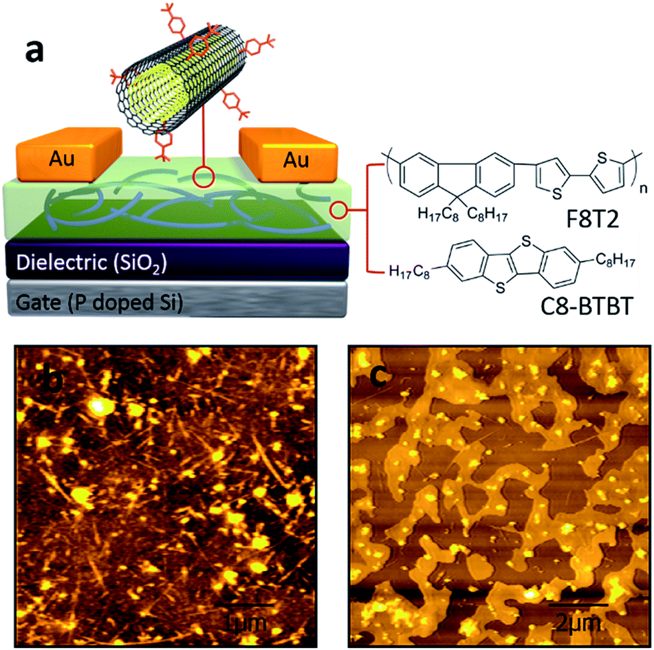 | ||
| Fig. 1 (a) Schematic diagram of the OFET device structure (left) and the chemical structures of the organic semiconductors, F8T2 and C8-BTBT, respectively (right). AFM images of (b) F8T2/f-DWCNTs film and (c) C8-BTBT/f-DWCNTs film. | ||
As shown in Fig. 1b and c, f-DWCNTs were well dispersed in F8T2 film and C8-BTBT film, respectively, thanks to the good compatibility between the two materials. The functionalization of DWCNTs were realized by using 4-(tert-butyl)benzenediazonium as shown in Fig. 2a. Comparative Raman spectroscopy was carried out to study the pristine DWCNTs and f-DWCNTs (Fig. 2b). The integrated area of the disorder-induced mode (D band) around 1325 cm−1 increased obviously for f-DWCNTs and the D/G ratio (peak area ratio between the D band and the G band) increased from 0.36 to 0.56, which indicate the outer wall has been successfully functionalized. The electrical conductivities of DWCNTs and f-DWCNTs were also investigated by fabricating and testing two-electrode configuration device. Compared to DWCNTs, f-DWCNTs had a substantial decline in current, indicating a significant decrease in electrical conductivity (Fig. 2c). This reduced conductivity was due to degradation of the sp2 hybridized framework of the f-DWCNTs outer wall. With long alkyl chain, the chemical groups could help DWCNTs disperse well in organic solvent. The dispersions of f-DWCNTs with three different chemical groups in chlorobenzene were also studied. 1 mg f-DWCNTs with carboxyphenyl group, 4-tert-butylphenyl group and phenyl group were added to 2 ml of chlorobenzene, respectively, followed by ultrasonication for 10 min. The dispersion of f-DWCNTs with 4-tert-butylphenyl group was better than that of f-DWCNTs with the other two chemical groups, as shown in Fig. S2b.† The f-DWCNTs with 4-tert-butylphenyl group were thus used to fabricate organic semiconductor/f-DWCNTs hybrid FETs.
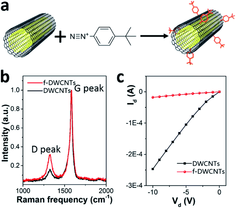 | ||
| Fig. 2 (a) Schematic of DWCNT functionalization. (b) Normalized Raman spectra of DWCNTs before (black line) and after (red line) functionalization. (c) I–V curves of DWCNTs before (black line) and after (red line) functionalization. | ||
Electrical performance of the hybrid OFETs
Fig. 3a shows transfer curves of F8T2 based pure OFET and hybrid OFETs, including F8T2/DWCNTs and F8T2/f-DWCNTs OFETs, with the drain voltage (Vd) fixed at −60 V. Both the hybrid OFETs exhibited higher source–drain current (Id) and threshold voltage (Vth) than those of pure OFET. The transportation of charge carriers in DWCNTs presents much longer mean free path as compared with that in organic semiconductors, which leads to a high Id for the hybrid device. Meanwhile, hole injection in the P-type hybrid OFETs was also improved by incorporation of DWCNTs, and Vth of the devices was thus increased. On the other hand, the two kinds of hybrid OFETs exhibited obviously different current on/off ratios. The on/off ratio of F8T2/DWCNTs OFETs dropped a lot, while that of F8T2/f-DWCNTs device retained almost the same as that of F8T2 pure OFET. We suggest that the better performance of the F8T2/f-DWCNTs hybrid devices can be assigned to following reasons: (a) f-DWCNTs are allowed to be well dispersed in the solution of organic semiconductor because of their much lower surface energy as compared to DWCNTs, leading to a better hybrid semiconducting film; (b) the benzene-based functional groups are allowed to form π bond conjugate system with organic semiconductor, and thus reduced the energy barrier for charge injection between f-DWCNTs and organic semiconductor. Fig. 3b and c shows the output characteristics of F8T2 based pure OFET and F8T2/f-DWCNTs OFET, respectively. The F8T2 based OFETs exhibited the electric performance of typical P-type devices, with both linear and saturation regime. The F8T2/f-DWCNTs OFET shown a much increased source–drain current compared with the pure F8T2 OFET in general, which gave further support to above conclusions. Fig. 3d shows the comparative transfer characteristics of C8-BTBT based pure OFETs and hybrid OFETs at a fixed Vd of −60 V. The source–drain current obtained a significant increase after the organic semiconductor incorporating with DWCNTs, which was in the similar situation as F8T2 based devices. The C8-BTBT/f-DWCNTs OFET exhibited even a higher on/off ratio than C8-BTBT based pure OFET, with a comparable off-current but a much higher on-current. The source–drain off-current of C8-BTBT/f-DWCNTs OFET retained as low as that of C8-BTBT based pure OFET in the low gate voltage range, because small amount of well-dispersed f-DWCNTs might disturb the morphology of the crystalline C8-BTBT film, and at the same time they provided “fast lanes” for charge carriers. The “fast lane” could just neutralize the adverse effects of the disturbed morphology when the C8-BTBT/f-DWCNTs OFET was on the off-state. As a small molecule organic semiconductor, C8-BTBT film often exhibits high crystallinity, while polymer organic semiconductor F8T2 is semicrystalline.29–31 When small amount of f-DWCNTs were incorporated into C8-BTBT film, the crystallinity of C8-BTBT was more affected than that of F8T2, leading a low off-current of C8-BTBT/f-DWCNTs OFET. For the on-state, the C8-BTBT/f-DWCNTs OFET exhibited source–drain current about four times higher than that of C8-BTBT based pure OFET, as transfer curves shown in Fig. 3d and output I–V curves shown in Fig. 3e and f. Therefore, incorporating f-DWCNTs with organic semiconductor is an effective route to enhance the performance for both F8T2 based OFETs and C8-BTBT based OFETs.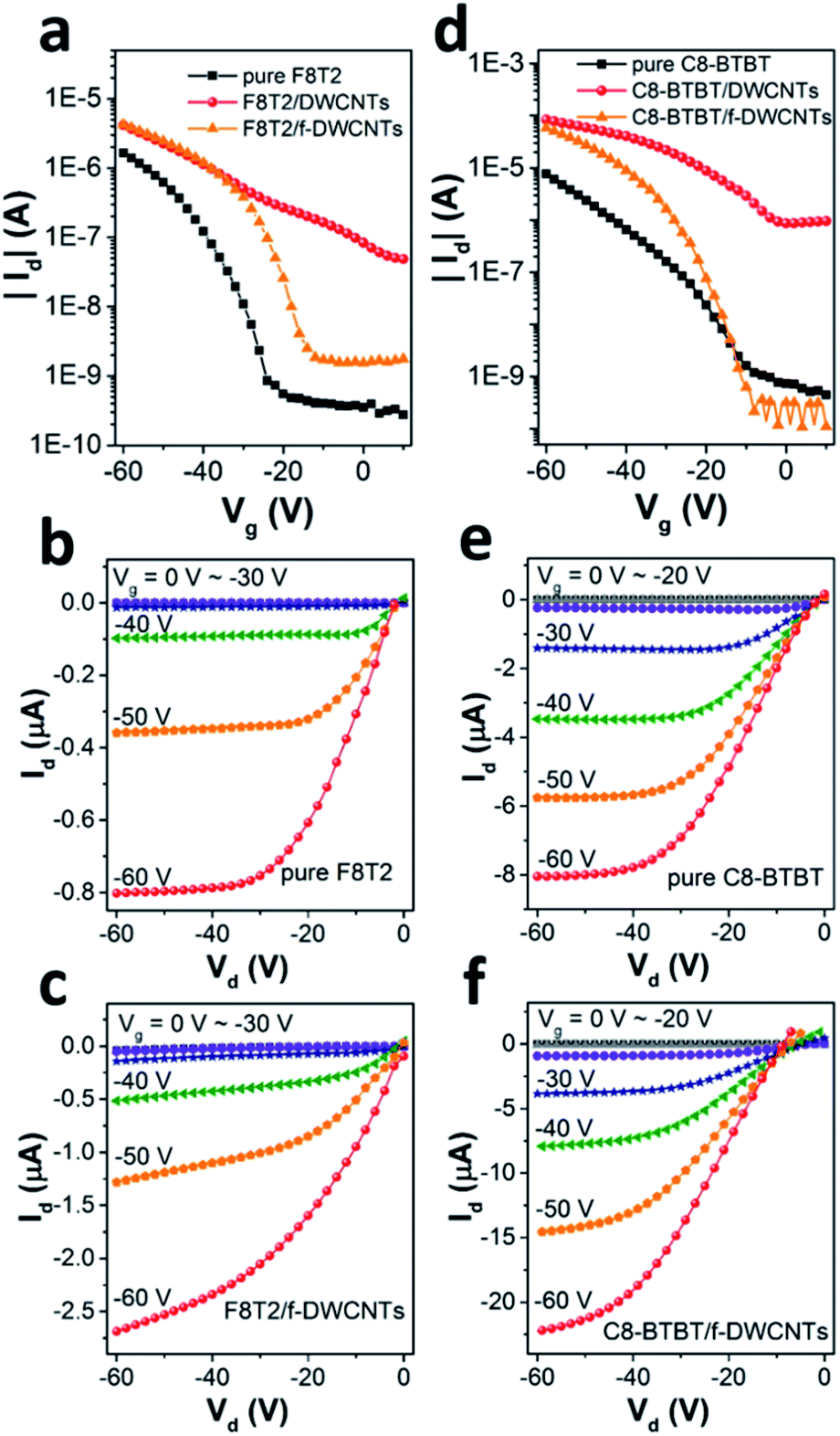 | ||
| Fig. 3 (a) Transfer characteristics of pure F8T2 device, F8T2/DWCNTs device and F8T2/f-DWCNTs device. Source–drain I–V curves of (b) pure F8T2 device and (c) F8T2/f-DWCNTs device. (d) Transfer characteristics of pure C8-BTBT devices, C8-BTBT/DWCNTs device and C8-BTBT/f-DWCNTs device. Source–drain I–V curves of (e) pure C8-BTBT device and (f) C8-BTBT/f-DWCNTs device. | ||
To study the dependence of device performance on f-DWCNTs dispersion concentration, organic semiconductor/f-DWCNTs hybrid films containing various densities of f-DWCNTs were also investigated. The transfer curves of F8T2/f-DWCNTs OFETs with different F8T2/f-DWCNTs mass ratio were shown in Fig. 4a (linear scale) and Fig. 4b (log scale). When a small amount of f-DWCNTs were added to F8T2, the device shown a slightly increased source–drain current (Id). As more f-DWCNTs were added, Id continued to increase while the on/off ratio began to decrease. The on/off ratio even dropped to a low of 20 since too much f-DWCNTs were added, which exceeded the percolation threshold of f-DWCNTs and an unwanted f-DWCNTs network formed. It seemed like that the unwanted f-DWCNTs network was formed more easily as F8T2 reduced (comparison of orange line and blue line in Fig. 4b), leading to the decrease of on/off ratio. Fig. 4c and d show transfer characteristics of C8-BTBT based OFETs incorporating with different amount of f-DWCNTs. A small amount of f-DWCNTs added to C8-BTBT could barely enhance device performance while too much f-DWCNTs leaded to a drastic drop in on/off ratio. Therefore, the electric performance of the hybrid OFETs can be optimized by adjusting the incorporating ratio of f-DWCNTs to organic semiconductor, and f-DWCNTs should be added below percolation threshold.
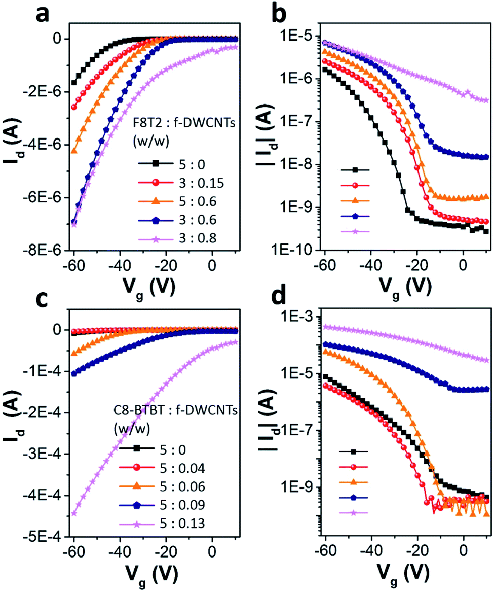 | ||
| Fig. 4 (a) Transfer curves of F8T2-based OFETs incorporating with various amount of f-DWCNTs in (a) linear scale and (b) log scale. Transfer curves of C8-BTBT-based OFETs incorporating with various amount of f-DWCNTs in (c) linear scale and (d) log scale. | ||
The device parameters of F8T2 based OFETs and C8-BTBT based OFETs are summarized in Table 1. Due to the morphology of organic semiconductor films was disturbed, the mobilities dropped slightly when a minimal amount of f-DWCNTs were added, as we discussed before. Then the mobilities increased as the f-DWCNTs were added more because f-DWCNTs were beneficial for charge carrier transport. However, the maximal values of mobility were not obtained while the maximal amount of f-DWCNTs were added. When the densities of added f-DWCNTs in organic semiconductor film were higher than the percolation threshold of f-DWCNTs, the on/off ratio dropped so low that the devices were not typical OFETs. Since the mobilities were extracted from OFET transfer curves, values of mobility might become less reliable when too much f-DWCNTs were added to the organic semiconductor. The obvious change of Vth showed a shift from negative to positive, which implies that charge injection was enhanced continuously as the amount of f-DWCNTs increased.32 Incorporating f-DWCNTs into organic semiconductor showed a significant impact on device behavior, and the degree of the impact is directly related to the amount of added f-DWCNTs.
| a | ||||
|---|---|---|---|---|
| F8T2/DCB (mg ml−1) | f-DWCNTs/CB (mg ml−1) | Mobility cm2 (V−1 s−1) | Vth (V) | On/off ratio |
| 5 | 0 | 0.0124 ± 0.0014 | −32 ± 2 | 5 × 10³ |
| 3 | 0.15 | 0.0116 ± 0.0012 | −23 ± 2 | 4 × 10³ |
| 5 | 0.6 | 0.0146 ± 0.0006 | −17 ± 1 | 3 × 10³ |
| 3 | 0.6 | 0.0213 ± 0.0008 | −14 ± 1 | 3 × 10² |
| 3 | 0.8 | 0.0103 ± 0.0014 | 1 ± 2 | 20 |
| b | ||||
|---|---|---|---|---|
| C8-BTBT/CB (mg ml−1) | f-DWCNTs/CB (mg ml−1) | Mobility cm2 (V−1 s−1) | Vth (V) | On/off ratio |
| 5 | 0 | 0.065 ± 0.002 | −34 ± 1 | 1 × 10⁴ |
| 5 | 0.04 | 0.022 ± 0.006 | −31 ± 3 | 6 × 10³ |
| 5 | 0.06 | 0.270 ± 0.059 | −28 ± 1 | 6 × 10⁵ |
| 5 | 0.09 | 0.132 ± 0.035 | 1 ± 13 | 13 |
| 5 | 0.13 | 0.262 ± 0.055 | 21 ± 8 | 5 |
Conclusions
In conclusion, we have demonstrated that by incorporating a suitable amount of f-DWCNTs into organic semiconductors, including both a polymeric semiconductor F8T2 and a small molecular semiconductor C8-BTBT, the electric performances of OFETs were significantly improved. As compared to unfunctionalized DWCNTs, the lower surface energy of f-DWCNTs allows them to be well-dispersed in solutions of organic semiconductor. Sufficient amount of f-DWCNT are thus allowed to be embedded into the semiconducting film to significantly increase the mobility, without obvious aggregation and decrease in the current on/off ratio of the device. Compared to conventional OFETs, the output source–drain currents of F8T2/f-DWCNTs and C8-BTBT/f-DWCNTs hybrid FETs could be increased, while the current on/off ratios of the hybrid devices retained comparable or exhibited even better than that of the pure OFETs. Meanwhile, the threshold voltage of the OFETs decreased due to charge injection enhancement by the f-DWCNTs. Hybrid OFET with optimized electric performance was then obtained through adjusting the incorporation ratio of the two materials. Therefore, incorporating organic semiconductors and f-DWCNTs into OFETs as active layers could be a broad applicable strategy to enhance the OFETs electric performances, which is expected to further reduce the distance from practical applications of flexible electronics.Acknowledgements
This work thanks the financial support by the National Nature Science Foundation of China (Grant No. 21302142 and 51603151), Science & Technology Foundation of Shanghai (14JC1492600, 14YF1403700), the Fundamental Research Funds for the Central Universities, and the 1000 youth talent plan. X. Wu also acknowledges the financial support from State Key Laboratory of ASIC & System (2016KF001).Notes and references
- X. Liu, Y. Guo, Y. Ma, H. Chen, Z. Mao, H. Wang, G. Yu and Y. Liu, Adv. Mater., 2014, 26, 3631 CrossRef CAS PubMed.
- G. Schwartz, B. C. Tee, J. Mei, A. L. Appleton, H. Kim do, H. Wang and Z. Bao, Nat. Commun., 2013, 4, 1859 CrossRef PubMed.
- J. Huang, H. Zhu, Y. Chen, C. Preston, K. Rohrbach, J. Cumings and L. Hu, ACS Nano, 2013, 7, 2106 CrossRef CAS PubMed.
- H. E. Katz and J. Huang, Annu. Rev. Mater. Res., 2009, 39, 71 CrossRef CAS.
- S. K. Gupta, P. Jha, A. Singh, M. M. Chehimi and D. K. Aswal, J. Mater. Chem. C, 2015, 3, 8468 RSC.
- X. Wu, Y. Ma, G. Zhang, Y. Chu, J. Du, Y. Zhang, Z. Li, Y. Duan, Z. Fan and J. Huang, Adv. Funct. Mater., 2015, 25, 2138 CrossRef CAS.
- Y.-p. Wen, D. Li, Y. Lu, H.-h. He, J.-k. Xu, X.-m. Duan and M. Liu, Chin. J. Polym. Sci., 2012, 30, 460 CrossRef CAS.
- J. Huang, J. Miragliotta, A. Becknell and H. E. Katz, J. Am. Chem. Soc., 2007, 129, 9366 CrossRef CAS PubMed.
- J. Huang, J. Sun and H. E. Katz, Adv. Mater., 2008, 20, 2567 CrossRef CAS.
- X. Wu and J. Huang, IEEE journal on emerging and selected topics in circuits and systems, 2016, 1 Search PubMed.
- Y. Chu, X. Wu, J. Lu, D. Liu, J. Du, G. Zhang and J. Huang, Adv. Sci., 2016, 3, 1500435 CrossRef PubMed.
- M. W. Alam, Z. Wang, S. Naka and H. Okada, Appl. Phys. Lett., 2013, 102, 061105 CrossRef.
- Z. Wang, M. W. Alam, Y. Lou, S. Naka and H. Okada, Appl. Phys. Lett., 2012, 100, 043302 CrossRef.
- Q. Zheng, J. Huang, A. Sarjeant and H. E. Katz, J. Am. Chem. Soc., 2008, 130, 14410 CrossRef CAS PubMed.
- S. Park, M. Vosguerichian and Z. Bao, Nanoscale, 2013, 5, 1727 RSC.
- C. Wang, K. Takei, T. Takahashi and A. Javey, Chem. Soc. Rev., 2013, 42, 2592 RSC.
- U. N. Maiti, W. J. Lee, J. M. Lee, Y. Oh, J. Y. Kim, J. E. Kim, J. Shim, T. H. Han and S. O. Kim, Adv. Mater., 2014, 26, 40 CrossRef CAS PubMed.
- S. R. Shin, R. Farzad, A. Tamayol, V. Manoharan, P. Mostafalu, Y. S. Zhang, M. Akbari, S. M. Jung, D. Kim, M. Comotto, N. Annabi, F. E. Al-Hazmi, M. R. Dokmeci and A. Khademhosseini, Adv. Mater., 2016, 28, 3280 CrossRef CAS PubMed.
- J. Huang, D. R. Hines, B. J. Jung, M. S. Bronsgeest, A. Tunnell, V. Ballarotto, H. E. Katz, M. S. Fuhrer, E. D. Williams and J. Cumings, Org. Electron., 2011, 12, 1471 CrossRef CAS.
- F. Schwierz, Nat. Nanotechnol., 2010, 5, 487 CrossRef CAS PubMed.
- L. Britnell, R. V. Gorbachev, R. Jalil, B. D. Belle, F. Schedin, A. Mishchenko, T. Georgiou, M. I. Katsnelson, L. Eaves, S. V. Morozov, N. M. Peres, J. Leist, A. K. Geim, K. S. Novoselov and L. A. Ponomarenko, Science, 2012, 335, 947 CrossRef CAS PubMed.
- Q. Cao, H. S. Kim, N. Pimparkar, J. P. Kulkarni, C. Wang, M. Shim, K. Roy, M. A. Alam and J. A. Rogers, Nature, 2008, 454, 495 CrossRef CAS PubMed.
- M. Wang, F. Jakubka, F. Gannott, M. Schweiger and J. Zaumseil, Org. Electron., 2014, 15, 809 CrossRef CAS.
- K. Balasubramanian and M. Burghard, Small, 2005, 1, 180 CrossRef CAS PubMed.
- J. Huang, A. L. Ng, Y. Piao, C. F. Chen, A. A. Green, C. F. Sun, M. C. Hersam, C. S. Lee and Y. Wang, J. Am. Chem. Soc., 2013, 135, 2306 CrossRef CAS PubMed.
- K. E. Moore, D. D. Tune and B. S. Flavel, Adv. Mater., 2015, 27, 3105 CrossRef CAS PubMed.
- A. A. Green and M. C. Hersam, ACS Nano, 2011, 5, 1459 CrossRef CAS PubMed.
- C. Shen, A. H. Brozena and Y. Wang, Nanoscale, 2011, 3, 503 RSC.
- H. Sirringhaus, R. J. Wilson, R. H. Friend, M. Inbasekaran, W. Wu, E. P. Woo, M. Grell and D. D. C. Bradley, Appl. Phys. Lett., 2000, 77, 406 CrossRef CAS.
- A. Salleo, M. L. Chabinyc, M. S. Yang and R. A. Street, Appl. Phys. Lett., 2002, 81, 4383 CrossRef CAS.
- H. Ebata, T. Izawa, E. Miyazaki, K. Takimiya, M. Ikeda, H. Kuwabara and T. Yui, J. Am. Chem. Soc., 2007, 129, 15732 CrossRef CAS PubMed.
- C. M. Aguirre, C. Ternon, M. Paillet, P. Desjardins and R. Martel, Nano Lett., 2009, 9, 1457 CrossRef CAS PubMed.
Footnote |
| † Electronic supplementary information (ESI) available. See DOI: 10.1039/c7ra03467a |
| This journal is © The Royal Society of Chemistry 2017 |