
 Open Access Article
 This Open Access Article is licensed under a
 Creative Commons Attribution 3.0 Unported Licence
Modelling of an equivalent circuit for Cu2ZnSnS4- and Cu2ZnSnSe4-based thin film solar cells†
Naoyuki Shibayama *a,
Yiwen Zhanga,
Tetsuo Satakea and
Mutsumi Sugiyamab
*a,
Yiwen Zhanga,
Tetsuo Satakea and
Mutsumi Sugiyamab
aTechnical Research Institute, Toppan Printing Co., Ltd., Sugito 345-8508, Japan. E-mail: naoyuki.shibayama@toppan.co.jp
bDepartment of Electrical Engineering, Faculty of Science and Technology, Tokyo University of Science, Noda 278-8510, Japan
First published on 11th May 2017
Abstract
The internal resistance and quality of the interface in Cu2ZnSn(S, Se)4 (CZT(S, Se)) solar cells were investigated using electrochemical impedance spectroscopy (EIS). We developed an equivalent circuit of the CZT(S, Se) solar cell involving the contact and material resistances Rbulk, two parallel resistances, and a ‘capacitance-like element’ called a constant phase element (CPE) around the CZT(S, Se)/CdS heterojunction and Mo–Mo(S, Se)2/CZT(S, Se) back-contact interfaces. Using the EIS method, the states of Mo(S, Se) and the CZT(S, Se) layer could be digitised non-destructively. This result can provide guidelines for improving the performance of CZT(S, Se) solar cells or any semiconductor device.
Introduction
Cu2ZnSn(S, Se)4 (CZT(S, Se)) materials have been extensively studied for use in next-generation solar cells because they can be produced with inexpensive materials and processes.1 The energy conversion efficiency of CZT(S, Se) solar cells has reached 12.6%;2 however, this is remarkably lower than that of cadmium telluride (CdTe, 22.1%) and copper indium gallium selenide (CIGS, 22.6%) based solar cells.3Many studies have been carried out to identify the major hurdles that influence the CZT(S, Se) solar cell performance, such as composition defects, interface energy band gap, and structure. In addition, the elimination or passivation of Cu–Zn disorder can be very important for improving the efficiency of CZT(S, Se) solar cells.4
It is widely accepted that charge recombination at the interface is one possible cause of Voc degradation.5 Therefore, understanding charge transfer and charge recombination at different interfaces is important for improving the performance of CZTS solar cells. It is reported that CZTS/CdS interface has shown a cliff configuration which contributes to carrier losses.6 On the other hand, the interface of Mo/Mo(S, Se)/CZT(S, Se) are the stage at which research is currently underway.
One strategy to enhance the performance of CZT(S, Se) solar cells are (1) to control the chemical composition of the CZT(S, Se) absorber layer to improve efficiency7 and (2) to modify the back contact/absorber8 and absorber/buffer9 layer interfaces. However, clear guidelines for the correlation between the device performance and internal issues such as the absorber layer and interface of the devices have not yet been established.
Electrochemical impedance spectroscopy (EIS) is a non-destructive technique for examining electrochemical devices using transfer functions10 such as the impedance of the equivalent circuits of CdTe,11 CIGS,12 dye-sensitised,13 and perovskite solar cells.14 The advantage of EIS is to provide comprehensive data to evaluate both the capacitance of the complex stacked layers and the quality and uniformity of the interfaces. In our previous studies, the EIS method was applied to investigate CIGS solar cells,12b–d and the state of the pn junction interface was confirmed, which are issues that are difficult to investigate using other techniques such as capacitance measurements, admittance spectroscopy, and deep-level transient spectroscopy.
In this study, we used EIS to investigate the internal situation of CZT(S, Se) solar cells and improve their photovoltaic performance. An experimental model was developed to compare the Mo(S, Se)2 thickness of CZT(S, Se) solar cells and examine defects in the CZT(S, Se) absorber layer. This study demonstrated that EIS can be used to characterise the CZT(S, Se)/CdS heterojunction and non-ohmic Mo–Mo(S, Se)2/CZT(S, Se) back-contact interfaces. Our findings can provide guidance to improving the performance of CZT(S, Se) solar cells.
Results and discussion
In general, an equivalent circuit of simple heterojunction materials consists of three elements: the contact and material resistances Rbulk, parallel circuit with the parallel resistance Rp, and constant capacitance C or capacitance-like element called a constant phase element (CPE). A CPE displays impedance with non-ideal frequency-dependent properties and a constant phase over the entire frequency. The non-ideal behaviour originates from the distribution of the current density due to material inhomogeneity.12b,c The impedance of a CPE (ZCPE) is defined by the CPE index p (CPE-p) and CPE constant T (CPE-T) as follows:
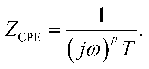 | (1) |
Fig. 1 shows Nyquist plots for each of the equivalent circuits. The horizontal axis (real axis) represents the resistance, and the normal axis (imaginary axis) represents the capacitance of the equivalent circuit. For the equivalent circuit using C, the diameter of the semicircle represents Rp, and the value of the intersection to the right of the semicircle and the horizontal axis represents Rbulk, as shown in Fig. 1(a). The Nyquist plot of the equivalent circuit using a CPE makes single semicircles with their centres lying below the imaginary axis, as shown in Fig. 1(b). Here, j is a complex number, and ω is the angular frequency. The value of CPE-p (where 0 ≤ p ≤ 1) reflects the uniformity and quality of the interface. As the value of CPE-p approaches 1, a higher-quality uniformity and interface can be ascertained by observing the cross section.
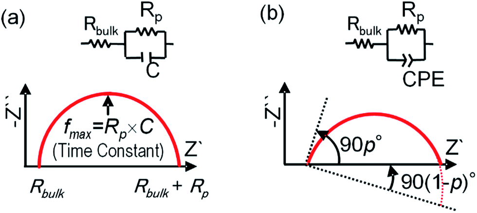 | ||
| Fig. 1 Equivalent circuits and Nyquist plots of simple heterojunction materials consisting of three elements: Rbulk, Rp, and (a) C or (b) CPE. | ||
As summarised in Table 1 and Fig. 2, conversion efficiencies of 4.25% and 0.75% were obtained for the CZTS and CZTSe solar cells, respectively. As shown in Fig. 3, the edge of external quantum efficiency (EQE) spectra of the CZTS and CZTSe solar cells were about 950 nm and 1280 nm, respectively. The EQE values obtained for CZTSe solar cell in the whole region is markedly remarkably lower than that for CZTS solar cell. Fig. 4 shows the X-ray diffraction (XRD) patterns of the Mo/MoS2/CZTS and Mo/MoSe2/CZTSe layers, respectively. In the Mo/MoS2/CZTS layer, CZTS crystal and Mo which are the substrate constituents were observed. On the other hand, in Mo/MoSe2/CZTSe layer, in addition to CZTSe and Mo, patterns derived from MoSe2 were observed. As a result of XRD, it was confirmed that selenium (Se) was not contained in the CZTS layer and sulfur (S) was not contained in the CZTSe layer. It was confirmed that Mo reacts more easily with Se than S.15 In both photoharvesting layers of CZTS and CZTSe, respective constituent elements copper (Cu), zinc (Zn), tin (Sn), sulfur (S) and selenium (Se) distribution is uniform and exist homogeneously. The distribution of each element in the film is shown in our previously published report.16
| Cell | Efficiency (%) | FF (—) | Voc (V) | Jsc (mA cm−2) |
|---|---|---|---|---|
| CZTS | 4.25 | 0.494 | 0.371 | 23.17 |
| CZTSe | 0.75 | 0.290 | 0.184 | 14.04 |
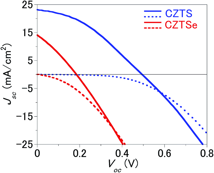 | ||
| Fig. 2 J–V curves of CZTS and CZTSe solar cells. | ||
 | ||
| Fig. 3 Measured EQE spectra of CZTS and CZTSe solar cells employed in this work. | ||
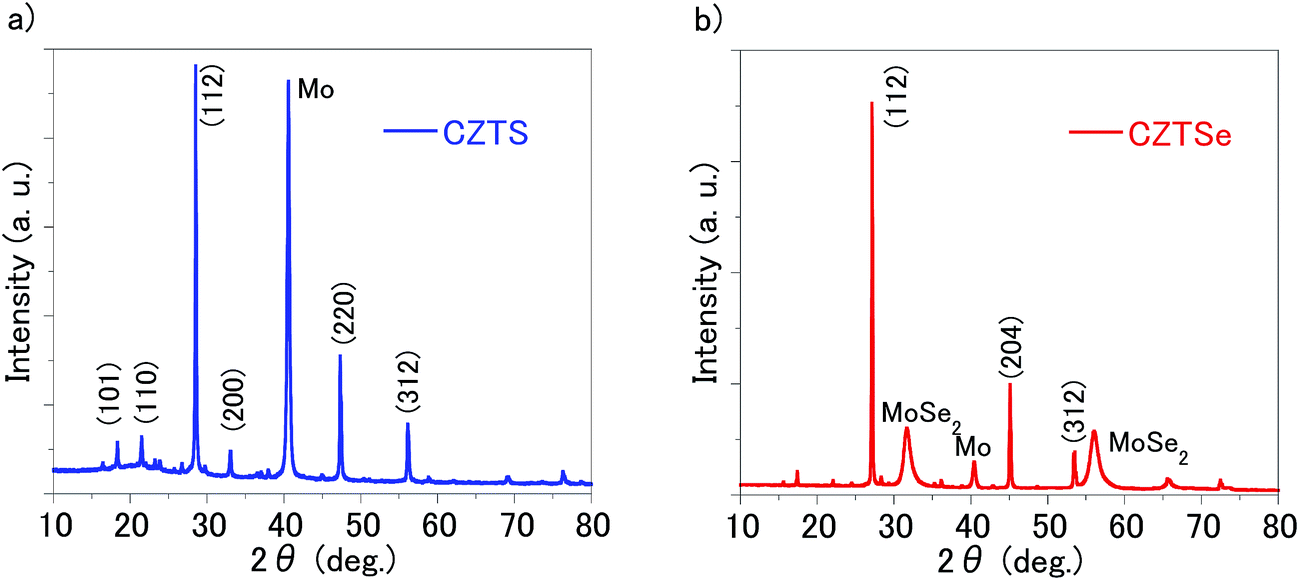 | ||
| Fig. 4 XRD patterns of (a) Mo/MoS2/CZTS and (b) Mo/MoSe2/CZTSe layers. | ||
A cross-sectional Scanning Ion Microscope (SIM) with a slope of 60 degrees is shown in Fig. 5. The thickness of the absorption layers in CZTS and CZTSe are measured to be around 1.3 μm and 1.5 μm for the CZT(S, Se) layer respectively. In our previous study, a possible interpretation for this much poorer performance of the CZTSe solar cell is that Cu-rich regions in the CZTSe layer provide a leakage current path.16 The thickness of the Mo(S, Se)2 layer compared with that of the CZTS solar cell may be another reason for the low efficiency of the CZTSe solar cell.8d To obtain further insight into the performances of CZTS and CZTSe solar cells, EIS was used to measure the resistance and quality of the thick CZT(S, Se)/CdS heterojunction and non-ohmic Mo–Mo(S, Se)2/CZT(S, Se) back contact interfaces of CZTS and CZTSe solar cells.
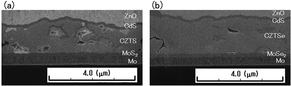 | ||
| Fig. 5 SIM image of cross-sectional surface of (a) CZTS_cell and (b) CZTSe_cell. | ||
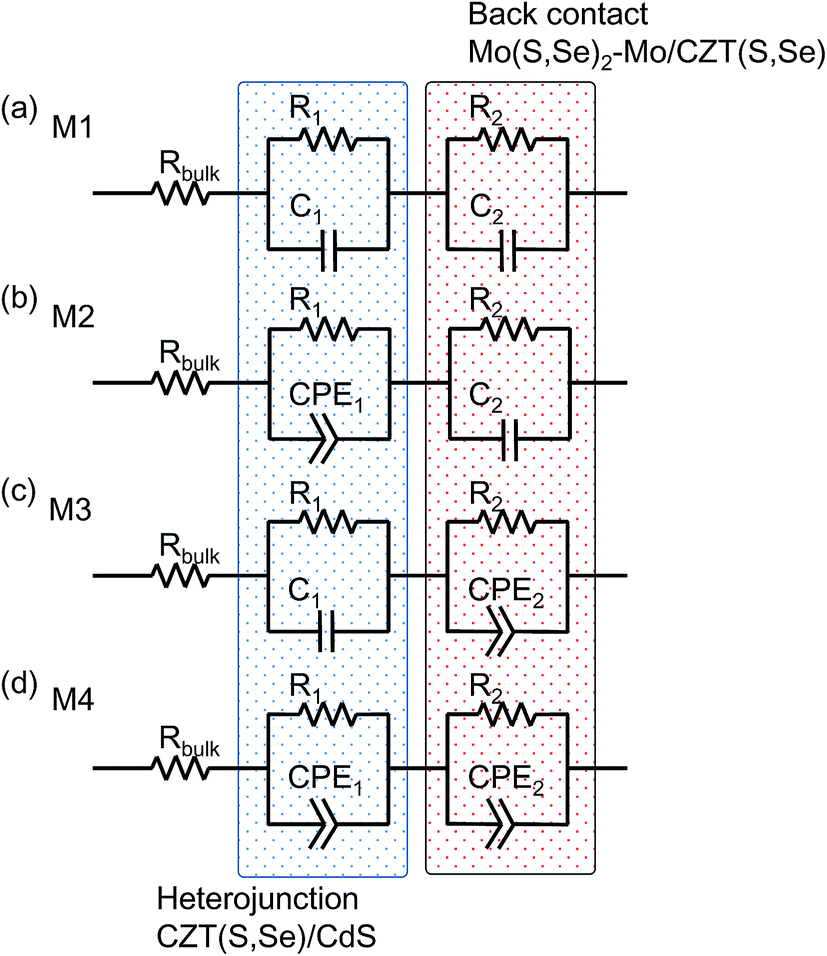
Fig. 6 shows the four equivalent circuit models tested to adjust the impedance data: M1–M4. The simplest model (M1) corresponded to a device characterised by the contact and material resistances Rbulk and two consecutive circuit elements consisting of a capacitor and resistor in parallel (C1–R1, C2–R2). The first element modelled all of the contact and material resistances Rbulk, such as the Mo contact, ZnO:Al front window, and Ag:Mo contact grid. The capacitors and resistors in parallel corresponding to the low- and high-frequency sides of the Nyquist plots described the CZT(S, Se)/CdS heterojunction (Fig. 6, shaded by the blue box) and the non-ohmic Mo–Mo(S, Se)2/CZT(S, Se) electrical back contact (Fig. 6, shaded by red box) in the AC response, respectively. Model M1 defined that the chemical composition and shape around the CZT(S, Se)/CdS and Mo–Mo(S, Se)2/CZT(S, Se) interfaces are uniform. The second model (M2) replaced C1–R1 of M1 with CPE1–R1. M2 defined that the chemical composition and shape around the CZT(S, Se)/CdS heterojunction interface was non-uniform. The third model (M3) replacedC2–R2 of M1 with CPE1–R1. M3 defined that the chemical composition and shape around the Mo–Mo(S, Se)2/CZT(S, Se) interface were non-uniform. The last model (M4) replaced C1–R1 and C2–R2 of M1 with CPE1–R1 and CPE2–R2, respectively. M4 defined that the chemical composition and shape around the CZT(S, Se)/CdS and Mo–Mo(S, Se)2/CZT(S, Se) interfaces were non-uniform.
 | ||
| Fig. 6 Tested equivalent circuits of the CZTS and CZTSe solar cells. | ||
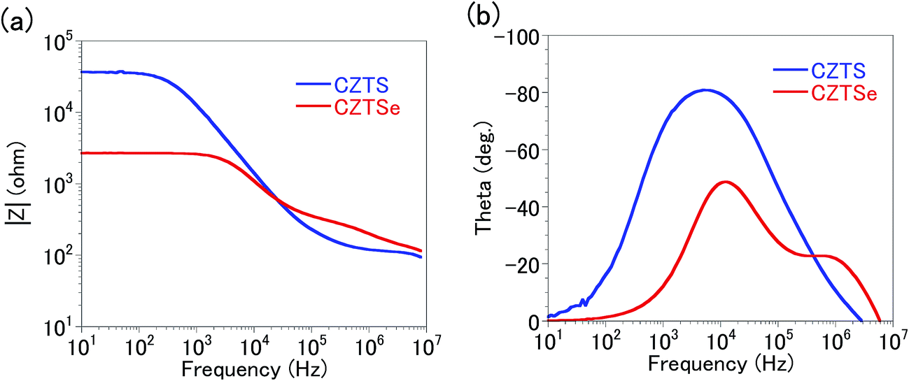
Fig. 7 shows Bode plots of the impedances of the CZTS and CZTSe solar cells. There were two critical frequencies with magnitudes of around 103 to 104 and 105 to 106 Hz for the CZT(S, Se)/CdS and Mo–Mo(S, Se)2/CZT(S, Se) interfaces, respectively. This result is consistent with the admittance spectroscopy result.17 The CZTS and CZTSe solar cells were confirmed to be composed of Rbulk and two parallel assemblies of C–R or CPE-R. In other words, they can be represented by any of the four equivalent circuit models in Fig. 6.
 | ||
| Fig. 7 Bode plots of CZTS and CZTSe solar cells: (a) amplitude |Z| and (b) phase. | ||
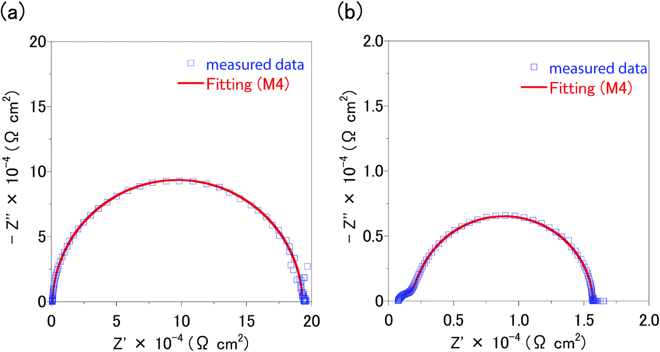
Fig. 8, S1 and S2† show the Nyquist plots and fitting results for the impedances of the CZTS and CZTSe solar cells. The chi-squared function (χ2) provides a good indication of the quality adaptation; a lower value indicates a better match rate.18 As a result of the fitting, it was found that M4 is the most suitable equivalent circuit model. The Mo(S, Se)2 layer has a graded structure in which the proportions of S and Se decrease and the proportion of Mo increases as the Mo layer is approached; further, Cu is added.16 Fig. 2 shows that the J–V curves of both CZT(S, Se) solar cells cause crossovers. Thus, the resistance near the interface of the Mo(S, Se)2/CZT(S, Se) layer is high. In other words, the region close to the interface between the thick Mo(S, Se)2 layer and CZT(S, Se) layer in particular has a heterogeneous composition. Consequently, because CPE2–R2 was selected for Mo–Mo(S, Se)2/CZT(S, Se), M3 and M4 are compatible equivalent circuit models. Because the CZTS layer at the CZT(S, Se)/CdS interface was coated with the spray method, the interface shape tended to become uneven. Moreover, a large number of point defects and boundaries are present. Therefore, CPE1–R1 becomes the optimum combination of capacitances and resistances at the CZT(S, Se)/CdS interface. Thus, the equivalent circuit models M2 and M4 were selected. As a result of fitting and interface, the M4 was selected as the equivalent circuit model of the CZTS and CZTSe solar cells.
 | ||
| Fig. 8 Nyquist plots and fitting results of (a) CZTS and (b) CZTSe solar cells. | ||
EIS was performed under dark conditions to obtain further insight into the interface properties of the CZTS and CZTSe solar cells. Table 2 presents the corresponding EIS parameters. The value of the resistance R2 around the Mo–Mo(S, Se)2/CZT(S, Se) interface in the CZTS solar cell was 2.8 × 10² Ω cm2, which is 5.5 times less the value of that obtained for the CZTSe solar cell (1.7 × 10³ Ω cm2). Based on the results of the cross-sectional SIM images, the CZTSe solar cell had a thicker Mo(S, Se)2 layer than the CZTS solar cells. This result is consistent with the EIS results. The CZTSe solar cell was observed to have a CPE1-p value lower than that of the CZTS solar cell. This is because that thicker Mo(S, Se)2 layer should lower the uniformity and quality of the Mo–Mo(S, Se)2/CZT(S, Se) interface. The value of the resistance R1 around the CZT(S, Se)/CdS interface in the CZTS solar cell was 1.9 × 10⁵ Ω cm2, and the value obtained for the CZTSe solar cell (1.3 × 10⁴ Ω cm2) was 7% of that CPE2-p indicates the state of the CZT(S, Se)/CdS interface, and its values for the CZTS and CZTSe solar cells were nearly identical. A CdS layer was fabricated by the same procedure. The resistance R1 was considered to be influenced by the CZT(S, Se) layer. Our previous results showed that Cu-rich regions of the CZT(S, Se) layer provide a leakage current path in the CZTSe cells.16 Therefore, the value of the resistance R1 in the CZTSe solar cell was considered to be less than that expected from the leakage current paths.
| Cell | Rbulk (Ω cm2) | R1 (Ω cm2) | CPE1-p (—) | R2 (Ω cm2) | CPE2-p (—) |
|---|---|---|---|---|---|
| CZTS | 6.2 × 10² | 1.9 × 10⁵ | 0.983 | 2.8 × 10² | 0.954 |
| CZTSe | 5.4 × 10² | 1.3 × 10⁴ | 0.972 | 1.7 × 10³ | 0.591 |
Conclusions
We used EIS to develop an equivalent circuit model for CZT(S, Se) solar cells. By using the EIS method, it was demonstrated that the causes of the performance degradation of the CZT(S, Se) solar cells are the leakage current path in the CZT(S, Se) layer, the resistance, and the lower uniformity and quality of the thicker Mo(S, Se)2 layer. In other words, via analysis with the EIS method, it was possible to formulate guidelines for non-destructively improving the performance of CZT(S, Se) solar cells. We are able to suggest one of the guidelines for improving the conversion efficiency of CZT(S, Se) solar cells. Moreover the scope of this paper lies in devising a model for further understanding and advancement in the existing technology. This suggests that the abundance of experience and knowledge gained through the development of high-efficiency conventional solar cells can be applied to CZT(S, Se) solar cells.Experimental section
Materials and measurement
CuI, ZnI2, SnI4, and Se were purchased from Sigma-Aldrich Co. LLC. S, and Na2Se were purchased from Kojundo Chemical Lab. Co., Ltd. NaSe and thiourea were purchased from Kanto Chemical Co., Inc. All solvents and reagents were of the highest quality available and were used as received.The photocurrent–voltage (J–V) characteristics of the CZTS and CZTSe solar cell were measured on a Keithley 2611A source meter under irradiation of AM 1.5, 100 mW cm−2 (1 sun) supplied by a solar simulator (Otento-SunIII, Bunkoukeiki Co., Ltd.). The incident light intensity was calibrated with a reference Si solar cell (SRC-1000-RTD-XL-J, VLSI Standards. Incorporated). The active areas of the solar cells were determined with a KEYENCE VHX-1000 digital microscope.
The impedance was measured with an NF FRA5087 frequency response analyser at frequencies of 100 mHz to 1 MHz. For all measurements, an AC 100 mV signal was applied to the device without a DC bias under dark conditions at room temperature. The obtained data were fitted with the Z-plot software.
Preparation of CZTS and CZTSe solar cells
CZT(S, Se) solar cells were fabricated following the same experimental conditions and protocol in the previously published literature.16CuI (2.88 mmol), ZnI2 (1.76 mmol), and SnI4 (1.60 mmol) were added to pyridine(500 mL) as a metal source and then cooled to 0 °C by stirring until a clear solution was obtained. Na2Se (6.4 mmol), a chalcogenide source, was dissolved in methanol (125 mL) and then quickly transferred into the metal source to synthesize CZTSe nanoparticles, as shown in the following reaction: 1.8CuI + 1.1ZnI2 + SnI4 + 4Na2Se → Cu1.8Zn1.1Sn1.0Se4 + 8NaI. The reaction was carried out under N2 atmosphere at 0 °C for 30 min. The products were centrifuged and washed three times with solvent (pyridine–methanol = 4![[thin space (1/6-em)]](https://www.rsc.org/images/entities/char_2009.gif) :1) to remove the byproduct of NaI. The products were dispersed into pyridine/methanol solvents by sonication for 20 min. The cation ratios of the CZTSe nanoparticles (denoted as CZTSe nanoparticles) measured by EDS were Cu/(Zn + Sn) = 0.80 and Zn/Sn = 1.11. Thiourea was added into the as-synthesized CZTSe nanoparticles as a binder followed by spraying onto Mo-coated substrates heated at 250 °C using an ultrasonic spray system (Sono-Tek Exacta Coat). Then, sintering treatments were carried out under sulfur or selenium atmospheres. For sintering, the samples were placed in a quartz box of 16 cm3 volume and then sintered at 580 °C for 20 min under N2 atmosphere at atmospheric pressure. To prevent the loss of Sn and S during the sintering process, 10 mg of Sn powder and 48 mg of S powder were added in the box. For selenium sintering, the process was the same as that of sulfur sintering except that 10 mg of Sn and 40 mg of Se were used.
:1) to remove the byproduct of NaI. The products were dispersed into pyridine/methanol solvents by sonication for 20 min. The cation ratios of the CZTSe nanoparticles (denoted as CZTSe nanoparticles) measured by EDS were Cu/(Zn + Sn) = 0.80 and Zn/Sn = 1.11. Thiourea was added into the as-synthesized CZTSe nanoparticles as a binder followed by spraying onto Mo-coated substrates heated at 250 °C using an ultrasonic spray system (Sono-Tek Exacta Coat). Then, sintering treatments were carried out under sulfur or selenium atmospheres. For sintering, the samples were placed in a quartz box of 16 cm3 volume and then sintered at 580 °C for 20 min under N2 atmosphere at atmospheric pressure. To prevent the loss of Sn and S during the sintering process, 10 mg of Sn powder and 48 mg of S powder were added in the box. For selenium sintering, the process was the same as that of sulfur sintering except that 10 mg of Sn and 40 mg of Se were used.
Finally, solar cells with a structure of Al grid/B-doped ZnO/i-ZnO/CdS/CZT(S, Se)/Mo/soda-lime glass were fabricated. Here, CdS buffer layers were deposited by chemical bath deposition (CBD). Intrinsic ZnO and B-doped ZnO layers were deposited by metal organic chemical vapor deposition (MOCVD). Al grid electrodes were deposited by vacuum evaporation. The structure of the fabricated CZT(S, Se) solar cells are Mo/Mo(S, Se)2/CZT(S, Se)/CdS/ZnO/Al respectively. The area of the solar cell measured for photovoltaic performance was about 0.125 cm2.
Acknowledgements
The authors thank N. Suyama, and Professor A. Yamada for discussions. This research was partially supported by the Japan Science and Technology Agency, Advanced Low Carbon Technology Research and Development Program.References
- (a) S. Ito, Wiley Interdiscip. Rev.: Energy Environ., 2015, 4, 51 CrossRef CAS; (b) H. Zhou, W.-C. Hsu, H.-S. Duan, B. Bob, W. Yang, T.-B. Song, C.-J. Hsu and Y. Yang, Energy Environ. Sci., 2013, 6, 2822 RSC; (c) K. Kaur, N. Kumara and M. Kumar, J. Mater. Chem. A, 2017, 5, 3069 RSC.
- W. Wang, M. T. Winkler, O. Gunawan, T. Gokmen, T. K. Todorov, Y. Zhu and D. B. Mitzi, Adv. Energy Mater., 2014, 4, 1301465 CrossRef.
- M. A. Green, K. Emery, Y. Hishikawa, W. Warta, E. D. Dunlop, D. H. Levi and A. W. Y. Ho-Baillie, Prog. Photovoltaics, 2017, 1, 3 Search PubMed.
- (a) S. Susan, Sol. Energ. Mat. Sol. Cells, 2011, 95, 1482 CrossRef; (b) A. Walsh, S. Chen, S.-H. Wei and X.-G. Gong, Adv. Energy Mater., 2012, 2, 400 CrossRef CAS.
- O. Gunawana, T. K. Todorov and D. B. Mitzi, Appl. Phys. Lett., 2010, 97, 233506 CrossRef.
- (a) S. Siebentritt, Thin Solid Films, 2013, 535, 1 CrossRef CAS; (b) A. Polizzotti, I. L. Repins, R. Noufi, S.-H. Wei and D. B. Mitzi, Energy Environ. Sci., 2013, 6, 3171 RSC; (c) C. Yan, F. Liu, N. Song, B. K. Ng, J. A. Stride, A. Tadich and X. Hao, Appl. Phys. Lett., 2014, 104, 173901 CrossRef; (d) M. Courel, J. A. Andrade-Arvizu and O. Vigil-Galán, Appl. Phys. Lett., 2014, 105, 233501 CrossRef.
- (a) T. Toyama, T. Konishi, Y. Seo, R. Tsuji, K. Terai, Y. Nakashima, H. Okamoto and Y. Tsutsumi, Appl. Phys. Express, 2013, 6, 075503 CrossRef; (b) D.-H. Son, D.-H. Kim, S.-N. Park, K.-J. Yang, D. Nam, H. Cheong and J.-K. Kang, Chem. Mater., 2015, 27, 5180 CrossRef CAS; (c) W.-C. Chen, C.-Y. Chen, V. Tunuguntla, S. H. Lu, C. Su, C.-H. Lee, K.-H. Chen and L.-C. Chen, Nano Energy, 2016, 30, 762 CrossRef CAS; (d) Y. Qu, G. Zoppi and N. S. Beattie, Sol. Energ. Mat. Sol. Cells, 2016, 158, 130 CrossRef CAS; (e) J. Tao, K. Zhang, C. Zhang, L. Chen, H. Cao, J. Liu, J. Jiang, L. Sun, P. Yang and J. Chu, Chem. Commun., 2015, 51, 10337 RSC; (f) J. Tao, J. Liu, L. Chen, H. Cao, X. Meng, Y. Zhang, C. Zhang, L. Sun, P. Yang and J. Chu, Green Chem., 2016, 18, 550 RSC.
- (a) B. Shin, Y. Zhu, N. A. Bojarczuk, S. Jay Chey and S. Guha, Appl. Phys. Lett., 2012, 101, 053903 CrossRef; (b) A. Fairbrother, E. Garcia-Hemme, V. Izquierdo-Roca, X. Fontane, F. A. Pulgarin-Agudelo, O. Vigil-Galan, A. Perez-Rodriguez and E. Saucedo, J. Am. Chem. Soc., 2012, 34, 8018 CrossRef PubMed; (c) S. Lopez-Marino, M. Espíndola-Rodríguez, Y. Sánchez, X. Alcobé, F. Oliva, H. Xie, M. Neuschitzer, S. Giraldo, M. Placidi, R. Caballero, V. Izquierdo-Roca, A. Pérez-Rodríguez and E. Saucedo, Nano Energy, 2016, 26, 708 CrossRef CAS; (d) J. Li, Y. Zhang, W. Zhao, D. Nam, H. Cheong, L. Wu, Z. Zhou and Y. Sun, Adv. Energy Mater., 2015, 5, 1402178 CrossRef.
- (a) H. Katagiri, K. Jimbo, S. Yamada, T. Kamimura, W. S. Maw, T. Fukano, T. Ito and T. Motohiro, Appl. Phys. Express, 2008, 1, 041201 CrossRef; (b) S. Tajima, M. Umehara and T. Mise, Jpn. J. Appl. Phys., 2016, 55, 112302 CrossRef; (c) F. Jiang, C. Ozaki, Gunawan, T. Harada, Z. Tang, T. Minemoto, Y. Nose and S. Ikeda, Chem. Mater., 2016, 28, 3283 CrossRef CAS; (d) F. Liu, C. Yan, J. Huang, K. Sun, F. Zhou, J. A. Stride, M. A. Green and X. Hao, Adv. Energy Mater., 2016, 6, 1600706 CrossRef; (e) Y. Ren, J. J. S. Scragg, M. Edoff, J. K. Larsen and C. Platzer-Björkman, ACS Appl. Mater. Interfaces, 2016, 8, 18600 CrossRef CAS PubMed.
- (a) J. Bisquert, Phys. Chem. Chem. Phys., 2011, 13, 4679 RSC; (b) I. Mora-Seró, G. Garcia-Belmonte, P. P. Boix, M. A. Vázquezb and J. Bisquert, Energy Environ. Sci., 2009, 2, 678 RSC.
- B. H. Hamadani, J. Roller, P. Kounavis, N. B. Zhitenev and D. J. Gundlach, Sol. Energ. Mat. Sol. Cells, 2013, 116, 126 CrossRef CAS.
- (a) W.-J. Lee, H.-J. Yu, J.-H. Wi, D.-H. Cho, W. S. Han, J. Yoo, Y. Yi, J.-H. Song and Y.-D. Chung, ACS Appl. Mater. Interfaces, 2016, 8, 22151 CrossRef CAS PubMed; (b) M. Sugiyama, M. Hayashi, C. Yamazaki, N. B. Hamidon, Y. Hirose and M. Itagaki, Thin Solid Films, 2013, 535, 287 CrossRef CAS; (c) M. Sugiyama, H. Sakakura, S. W. Chang and M. Itagaki, Electrochim. Acta, 2014, 131, 236 CrossRef CAS; (d) H. Sakakura, M. Itagaki and M. Sugiyama, Jpn. J. Appl. Phys., 2016, 55, 012301 CrossRef.
- (a) N. Shibayama, H. Ozawa, Y. Ooyama and H. Arakawa, Bull. Chem. Soc. Jpn., 2015, 88, 366 CrossRef; (b) N. Shibayama, H. Ozawa, M. Abe, Y. Ooyama and H. Arakawa, Chem. Commun., 2014, 50, 6398 RSC; (c) Y. Adachi, Y. Ooyama, N. Shibayama and J. Ohshita, Dalton Trans., 2016, 45, 13817 RSC.
- (a) K. Miyano, M. Yanagida, N. Tripathi and Y. Shirai, Appl. Phys. Lett., 2016, 106, 093903 CrossRef; (b) I. Zarazua, G. Han, P. P. Boi, S. Mhaisalkar, F. Fabregat-Santiago, I. Mora-Seró, J. Bisquert and G. Garcia-Belmonte, J. Phys. Chem. Lett., 2016, 7, 5105 CrossRef CAS PubMed.
- M. Ganchev, Thin Solid Films, 2011, 519, 7394 CrossRef CAS.
- Y. Zhang, N. Suyama, M. Goto, J. Kuwana, K. Sugimoto, T. Satake, Y. Kurokawa, M. Yin and A. Yamada, Jpn. J. Appl. Phys., 2015, 54, 08KC05 CrossRef.
- (a) P. A. Fernandes, A. F. Sartori, P. M. P. Salome, J. Malaquias, A. F. da Cunha, M. P. F. Grac and J. C. Gonzalez, Appl. Phys. Lett., 2012, 100, 233504 CrossRef; (b) P. A. Fernandes, P. M. P. Salome, A. F. Sartori, J. Malaquias, A. F. Cunha, B. A. Schubert, J. C. Gonzalez and G. M. Ribeiro, Sol. Energ. Mat. Sol. Cells, 2013, 115, 157 CrossRef CAS.
- M. Umeda, K. Dokko, Y. Fujita, M. Mohamedi, M. Umeda, I. Uchida and J. R. Selman, Electrochim. Acta, 2001, 47, 885 CrossRef CAS.
Footnote |
| † Electronic supplementary information (ESI) available. See DOI: 10.1039/c7ra02274c |
| This journal is © The Royal Society of Chemistry 2017 |