
 Open Access Article
 This Open Access Article is licensed under a
 Creative Commons Attribution 3.0 Unported Licence
3D multilayered plasmonic nanostructures with high areal density for SERS†
MinKyoung Lee‡
ab,
Tae Yoon Jeon‡c,
ChaeWon Muna,
Jung-Dae Kwona,
Jungheum Yuna,
Shin-Hyun Kimc,
Dong-Ho Kim*a,
Seung-Cheol Chang*b and
Sung-Gyu Park *a
*a
aAdvanced Functional Thin Films Department, Korea Institute of Materials Science (KIMS), Changwon, Gyeongnam 641-831, Korea. E-mail: sgpark@kims.re.kr; dhkim2@kims.re.kr; Fax: +82-55-280-3570; Tel: +82-55-280-3632
bInstitute of BioPhysio Sensor Technology, Graduate Department of Molecular Science Technology, Pusan National University, Busan 46241, Korea. E-mail: s.c.chang@pusan.ac.kr
cDepartment of Chemical and Biomolecular Engineering (BK21+ Program), KAIST, Daejeon, 305-701, Korea
First published on 23rd March 2017
Abstract
Enhancing light–matter interactions is essential to improving nanophotonic and optoelectronic device performance. In the present work, we developed a new design for 3D plasmonic nanostructures with enhanced near-field interactions among the plasmonic nanomaterials. The 3D plasmonic nanostructures consisted of multilayered bottom Ag/polydimethylsiloxane (PDMS) nanostructures, an alumina middle layer, and top Ag nanoparticles (NPs). High areal density PDMS nanoprotrusions were self-organized by a simple maskless plasma etching process. The conformal deposition of alumina using atomic layer deposition and Ag deposition produced 3D plasmonic nanostructures. These structures induced multiple near-field interactions between the ultrahigh-areal-density (1400 μm−2) top Ag NPs and the underlying Ag nanostructures, and among the top Ag NPs themselves. The high density of hot spots across the 3D space yielded highly efficient and widely tunable plasmonic responses across the entire visible range. The SERS signal enhancement measured at the 3D plasmonic nanostructures was 3.9 times the signal measured at the 2D multilayered structures and 48.0 times the signal measured at a Ag NP layer deposited onto a Si substrate. Finally, the 3D plasmonic nanostructures exhibited excellent uniformity with a variation of 6.8%, based on a microscale Raman mapping analysis. The excellent Raman signal uniformity can be attributed to the ultrahigh areal density of the Ag NPs and the uniform thickness of the alumina spacing layer.
Introduction
Enhancing the optical response of a plasmonic nanomaterial under incident light is essential to improving the performances in nanophotonic and plasmonic device applications, such as photovoltaics,1 structural colour generation,2,3 photon detection,4 photocatalysis,5,6 solid-state lighting,7,8 and optical sensing.9,10 The structural design and composition of a plasmonic nanomaterial may be tuned to implement unique optical properties and concentrate light over nanoscale volumes.11 Recently, cost-effective multilayered plasmonic nanostructures consisting of a multilayered smooth metal film, a dielectric middle layer, and a top layer of metal nanoparticles (NPs), have been proposed as a means for inducing a strong optical response through the generation of localized surface plasmon resonance (LSPR).12–15 In these plasmonic nanostructures, the smooth bottom metal film acts as a reflective layer that induces near-field coupling between the top metal NPs and their mirror image at the bottom metal layer.16 The plasmonically active volume within which the electromagnetic (EM) field is highly concentrated is limited in these structures due to the small number density of hot spots generated on the flat 2D surface. The 2D metallic films may be expanded into high-density 3D plasmonic nanostructures to maximize the hot spot density and enhance the near-field interactions between plasmonic nanomaterials.Plasma etching is a standard fabrication technique in integrated circuit (IC) manufacturing processes. In an IC manufacturing process, a sacrificial dielectric pattern generated by photolithography is used as an etching mask to etch away the underlying semiconductor layer. Recently, randomly arrayed silicon nanorods were directly fabricated by plasma etching silicon without using an etching mask.17 The resulting silicon nanorods were then used to fabricate metallic nanostructures. This maskless plasma etching process has clear advantages in that it is an easy and fast process, amenable to high-throughput fabrication, and low in process cost compared to other nanolithographic processes. However, maskless silicon etching processes yield a low areal density (∼20 μm−2) of silicon nanopillars with a large gap distance. Therefore, capillary-driven leaning among the metal nanorods is then needed to induce near-field enhancement.17,18
Here, we report a new design for 3D plasmonic nanostructures with enhanced near-field interactions among the plasmonic nanomaterials that produce a highly efficient optical response across the full visible wavelength range and sensitive Raman sensing capabilities. High areal density (∼131 μm−2) Ag/polydimethylsiloxane (PDMS) nanostructures were self-organized by maskless plasma etching of the smooth PDMS surface and subsequent Ag evaporation. The conformal deposition of alumina using atomic layer deposition (ALD) and Ag deposition produced the 3D plasmonic nanostructures. During the decoration of the alumina-coated 3D Ag/PDMS hybrid nanostructures with a top layer of Ag NPs, the ultrahigh areal density (1400 μm−2) of Ag NPs were deposited onto the top surface and the sidewalls. These structures induced multiple near-field interactions between Ag NPs and the underlying Ag nanostructures, between the Ag NPs themselves on a single Ag bottom nanostructure, and between Ag NPs decorated onto the sidewalls of the two different adjacent structures. The ultrahigh density of hot spots across the 3D space yielded highly efficient and widely tunable plasmonic responses with a reflectance amplitude dip of 0.4–1.6% across the entire visible range. The near-field coupling generated among the high-density plasmonic nanomaterials on the 3D plasmonic nanostructures was found to be enhanced based on an analysis of the experimental SERS measurements and the theoretical simulations of the electric field enhancement. The SERS signal enhancement measured at the 3D plasmonic nanostructures was 3.9 times the signal measured at the 2D plasmonic nanostructures and 48.0 times the signal measured at a Ag NP layer deposited onto a Si substrate. The simulations predicted that the average value of the fourth power of the electric field enhancement at the 3D plasmonic nanostructures was 3.4 times the value at 2D multilayered structures and 38.5 times the value at the Ag NP layer on a smooth Si substrate. Finally, 3D plasmonic nanostructures exhibited an excellent Raman enhancement uniformity with standard deviation of 6.8%, based on a Raman mapping analysis. The ultrahigh density of Ag NPs and uniform thickness of alumina spacing layer allow for the excellent Raman signal uniformity.
Results and discussion
A schematic illustration of the overall process of fabricating the 3D plasmonic nanostructures is shown in Fig. 1a. First, PDMS nanoprotrusions were self-organized by maskless CF4 reactive ion etching (RIE) of a smooth PDMS substrate. PDMS is widely used in microfluidic systems because it is amenable to nanofabrication using soft lithography techniques, offers good chemical resistance, and it is biocompatible, optically transparent, flexible, and low in cost.19–21 Smooth PDMS surfaces are beneficial in microfluidics applications because the surfaces bond more tightly and light scattering at the surfaces is low. In our experiments, we utilized PDMS nanoprotrusions to generate ultrahigh-density plasmonic nanostructures. The 50 nm thick Ag nanostructures were directly grown onto PDMS nanoprotrusions via thermal evaporation. The density of the Ag NPs and the gap size between Ag NPs were controlled by tuning the PDMS dry etching conditions (ESI, Fig. S1†). After depositing the Ag bottom layer, a 10 nm thick alumina layer was deposited onto the Ag nanostructures by ALD. ALD techniques provide conformal deposition of compound thin films with atomic-scale thickness resolution through a self-limiting surface reaction.22,23 Lastly, the alumina/Ag nanostructured surfaces were decorated with Ag NPs to complete the fabrication of the 3D plasmonic nanostructures. An SEM image of the bottom Ag nanostructures formed by thermally evaporating a 50 nm Ag film onto the PDMS nanoprotrusions over a 75 s CF4 RIE period, is shown in Fig. 1b. The number density of Ag nanostructures was approximately 131 μm−2 (ESI, Fig. S2†). This number density was six times the number density generated by the maskless Si etching process17,18 and nanoimprint lithography.24–26 We optimized the RIE etching conditions and found that 75 s yielded a 30 nm gap size between Ag/PDMS hybrid nanostructures; this gap size is required for the subsequent deposition of the dielectric spacing layer and Ag NPs. Fig. 1c–f show the surface morphologies of the 3D plasmonic nanostructures, which featured a high density of Ag NPs on the alumina/Ag nanostructured surfaces. The density of Ag NPs depended on the thickness of the top evaporated Ag layer. Evaporated Ag layers clearly yielded ultrahigh-density Ag NPs of 1400 μm−2 (ESI, Fig. S2†). High-resolution cross-sectional images of the nanostructures on the 3D plasmonic nanostructures with top evaporated Ag layer 3 nm thick were collected using field emission transmission electron microscopy (FE-TEM), as shown in Fig. 1g. An alumina interlayer was conformally deposited onto the bottom Ag nanostructures via ALD. The excellent conformal deposition characteristics allowed the ALD-deposited alumina to be used as the optical tuning layer in the LSPR-based sensors.27 This layer also protected the SERS substrates.28 Interestingly, oblate elliptical top Ag NPs formed on the alumina surface due to the Volmer–Weber (VW) growth of Ag on the alumina. Noble metals, such as Ag or Au, are thermodynamically driven to cluster and form 3D particles on oxide surfaces.29,30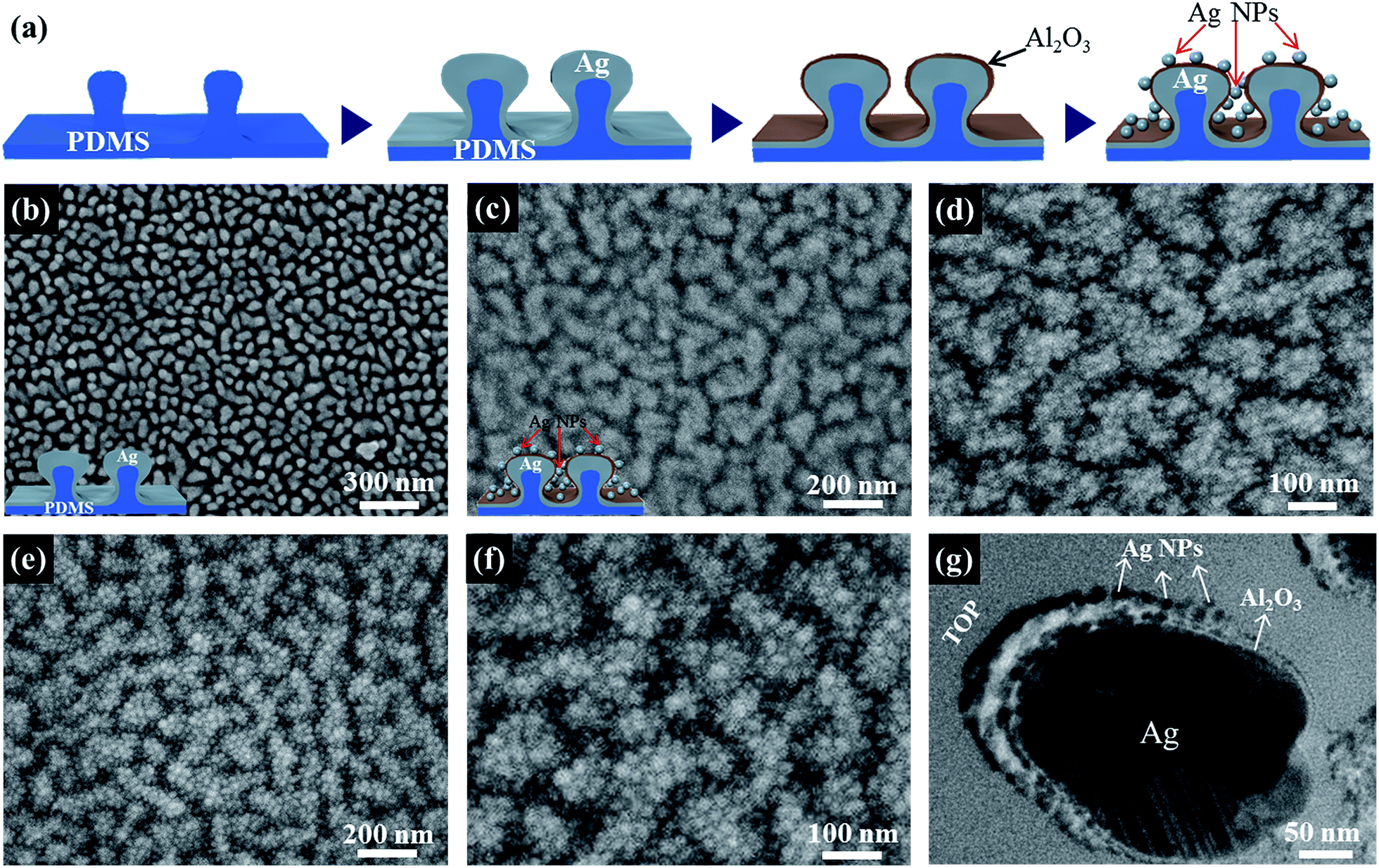 | ||
| Fig. 1 Fabrication of the 3D plasmonic nanostructures. (a) Schematic diagram illustrating the fabrication procedure used to generate 3D plasmonic nanostructures. (b) An SEM image collected after depositing 50 nm Ag onto the PDMS protrusions generated after 75 s CF4 RIE. The surface morphology changed as the top Ag layer thickness increased: (c) 3 nm, (d) 5 nm, and (e and f) 7 nm, given a constant 10 nm thick Al2O3 interlayer and 50 nm thick Ag bottom nanostructures. Ultrahigh-density Ag nanoparticles (1400 μm−2) and nanogaps were clearly observed on the 3D plasmonic nanostructures in (e). (g) A cross-sectional TEM image of a single 3D plasmonic nanostructure with top Ag layer thickness of 3 nm. | ||
Fig. 2 presents the optical reflectance properties of the 3D plasmonic nanostructures compared to those of conventional 2D plasmonic nanostructures. Fig. 2a is reflection photographs of large-area (2 × 2 cm2) 3D plasmonic nanostructures. The reflected colour varied depending on the LSPR frequency. The 50 nm thick Ag nanostructures grown directly onto PDMS nanoprotrusions were characterized by their own LSPR wavelength (with a reflectance dip amplitude of 6.3%) at 456 nm (black line, Fig. 2b), whereas the 50 nm thick flat Ag mirror deposited onto the smooth PDMS substrate did not generate an LSPR. Interestingly, the deposition of a 10 nm alumina interlayer and a subsequent top Ag NP layer dramatically changed the optical responses of the 3D plasmonic nanostructures (red line, Fig. 2b). A strong resonance with a low reflectance (R = 0.4%) was achieved from 484 nm to 662 nm, depending on the size of the top Ag NPs. Under plasmonic resonance conditions, the EM field was strongly enhanced and confined within both the dielectric interlayer in the plasmonic nanostructure and within the air nanogaps between top Ag NPs, leading to low reflection (or high absorption).12–14,30 Plasmonic coupling between the metal nanostructures led to a red shift in the LSPR wavelength. These results could be explained in terms of the hybridization of plasmons, which reduced the resonance energy (red-shifted the resonance wavelength).31 The effective diameters of the top Ag NPs increased, leading to an additional red shift in the LSPR wavelength. The bandwidth of the reflectance spectrum broadened as the evaporated Ag layer thickness increased due to the larger size distribution of top Ag NPs. Plasmonic nanostructures with a broad and high absorption across the full spectrum of visible light may be useful in a variety of applications, including plasmonic photovoltaics, photocatalysts, and SERS sensors. The amplitude of the reflectance dip increased with the evaporated Ag layer thickness due to light scattering from the large top Ag NPs (green line, Fig. 2b). Fig. 2c shows the reflectance spectra of conventional 2D nanostructures prepared by decorating a 10 nm thick alumina layer and 50 nm thick Ag film layer, supported by a flat PDMS substrate, with Ag NPs (ESI, Fig. S3† shows the surface morphologies of Ag NPs). The small Ag NPs conveyed to the 2D plasmonic nanostructure efficient optical properties with a reflectance of 1.0% at 482 nm, similar to results obtained previously from 2D multilayered plasmonic nanostructures;13 however, the optical properties deteriorated sharply as the Ag thickness increased due to the mirror-like reflection and scattering from the top Ag layer.
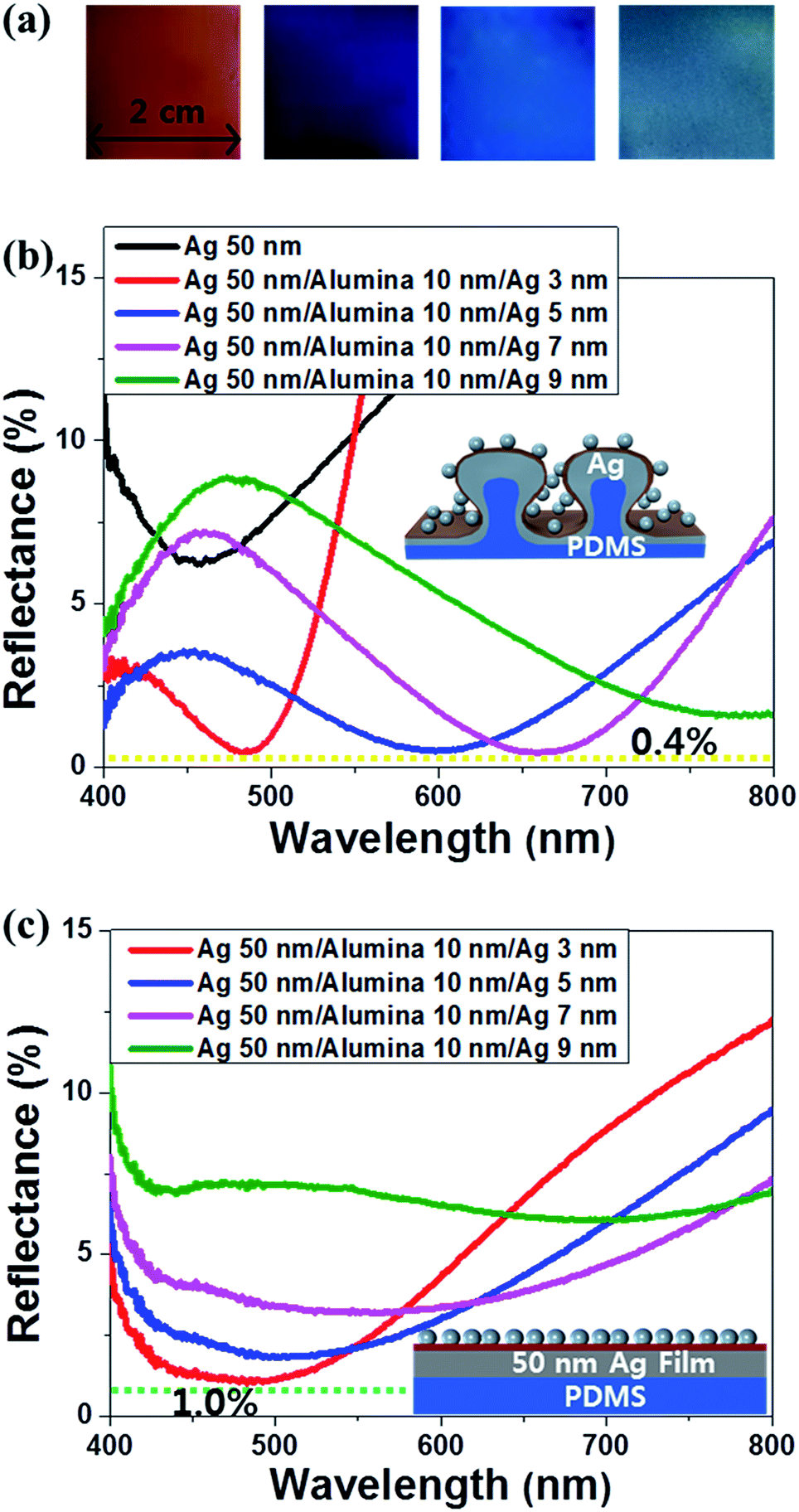 | ||
| Fig. 2 (a) Reflection photographs of a large-area (2 × 2 cm2) 3D plasmonic nanostructures with 3 nm, 5 nm, 7 nm and 9 nm thickness of top Ag layer (from left to right). Comparison of the optical properties of the (b) 3D and (c) 2D multilayered plasmonic nanostructures. | ||
A local EM field enhancement due to LSPR generation provides the main mechanism underlying signal amplification in the SERS technique.32 The ultrahigh density of hot spots in the 3D plasmonic nanostructure provided strong near-field enhancement, suggesting that this surface may be useful as an ultrasensitive SERS substrate. The tunable LSPR properties of our 3D plasmonic nanostructures convey distinct advantages for maximizing the SERS intensities of different target molecules. The SERS signal is optimized under conditions in which the excitation laser wavelength and Stokes-shifted Raman wavelength are both strongly enhanced. These conditions occur specifically when the LSPR wavelength is intermediate between the excitation and Stokes-shifted Raman wavelengths.33,34 Strong SERS signals were clearly observed in a monolayer of benzenethiol (BT) molecules adsorbed onto Ag NPs of different sizes (ESI, Fig. S4†). The 3D plasmonic nanostructures with an LSPR peak of 456 nm (prepared with a 3 nm thick Ag NP top layer) exhibited the smallest BT SERS intensity due to mismatch between the LSPR wavelength and the wavelengths of the incident beam and Stokes-shifted Raman signal. The 3D plasmonic nanostructure with an LSPR peak of 662 nm (prepared with a 7 nm thick Ag NP top layer) provided the best SERS performance, with a 632.8 nm incident laser beam.
Fig. 3a presents a comparison of the SERS signals collected at the 3D plasmonic nanostructures, 2D plasmonic nanostructures, and a Ag NP layer decorating a smooth Si substrate, at an excitation laser wavelength of λ = 632.8 nm. The 3D plasmonic nanostructures exhibited superior SERS performances compared to the 2D plasmonic nanostructures, regardless of the size of the top Ag NPs (ESI, Fig. S5†). Under optimized LSPR conditions, the 3D plasmonic nanostructure prepared with a 7 nm thick top Ag layer generated a BT SERS signal that was 3.9 times the signal generated at the 2D plasmonic nanostructures and 48.0 times the signal generated at the Ag NPs layer deposited onto the Si substrate (ESI, Fig. S6,† shows the surface morphologies of the Ag NPs deposited onto the smooth Si substrate). The electric field distribution across the 3D plasmonic nanostructure was calculated using finite-difference time-domain (FDTD) simulations, as shown in Fig. 3b. The linearly polarized 632.8 nm plane wave illumination beam were directed onto the plasmonic nanostructures. Field enhancements were generated through the three near-field coupling effects associated with coupling (1) between top Ag NPs and the underlying Ag nanostructures, (2) between the Ag NPs themselves on a single Ag bottom nanostructure, and (3) between Ag NPs decorated onto the sidewalls of the two different adjacent structures. The 3D plasmonic nanostructures are advantageous for plasmonic coupling compared to the 2D plasmonic nanostructures in that near-field coupling between the bottom Ag nanostructures and the Ag NPs deposited onto the sidewalls may be significantly enhanced due to the favourable alignment parallel to the polarization direction of the incident light. This alignment effect can be verified through laterally distributed high intensity regions of alumina interlayer of 3D plasmonic nanostructures. However, 2D plasmonic nanostructure has relatively low intensity at the alumina regions, because polarization direction of incident electric field is perpendicular to the arrangement between underlying Ag film and Ag NPs. The average SERS signal intensity is approximately proportional to the fourth power of the local electric field enhancement (i.e., |E|4/|E0|4, where |E0| and |E| are the incident and local electric field intensity). This equation was used to estimate SERS intensity variations by comparing the surface averaged values of |E|4/|E0|4 from three different plasmonic nanostructures, as shown in Fig. 3b–d. In many cases, this approximation is a good indicator of the order of magnitude of the SERS enhancement factor (EF).32 The average value of |E|4/|E0|4 for the 3D plasmonic nanostructure was 3.4 times the value obtained from the 2D plasmonic nanostructure and 38.5 times the value obtained from the Ag NPs on the smooth Si substrate. Interestingly, these theoretical values agreed well with the measured SERS signals intensities. The experimental and simulation results revealed that the 3D plasmonic nanostructure offers a superior structural design for generating strong near-field enhancement and highly sensitive SERS substrates.
 | ||
| Fig. 3 (a) SERS spectra measured from the benzenethiol (BT)-treated 3D plasmonic nanostructure (black line), 2D plasmonic nanostructure (red line), and Ag NPs on smooth Si substrate (blue line). The 3D plasmonic nanostructure generated BT SERS intensities that were 3.9 or 48.0 times the values produced on the 2D plasmonic nanostructure or Ag NPs on smooth Si substrate, respectively. The thickness of the top evaporated Ag NP layer was fixed at 7 nm for each SERS substrate. FDTD simulation of the electric field distributions across (b) the 3D plasmonic nanostructure, (c) 2D plasmonic nanostructure, and (d) Ag NPs decorated onto the smooth Si substrates at the wavelength of 632.8 nm. The nanogap between Ag NPs was held constant in all three plasmonic substrates. | ||
We found that the 3D plasmonic nanostructure exhibited excellent uniformity based on a microscale Raman mapping analysis. At an incident excitation wavelength of 632.8 nm using a 100× objective lens (NA 0.9), the spot area was calculated to be 0.58 μm2. A scan step of 1 μm was chosen to avoid pixel overlap. Fig. 4a shows a 2D Raman mapping of the BT Raman peak at 998 cm−1. A monolayer of BT molecules were adsorbed onto 3D plasmonic nanostructure. The total number of pixels is 121 (mapping area 11 × 11 μm2). Fig. 4b shows the SERS spectra of BT measured from the first row (pixels 1 to 11) of the Raman map. As shown in Fig. 4c and d, every pixel shows a uniform peak intensity for each Raman mode (i.e., 998, 1020 and 1070 cm−1). The standard deviation (SD) for each Raman mode is less than 7.0%. We also investigated SERS signal uniformity (SD 11.4%) for a 2 μM BT-treated 3D plasmonic nanostructure (ESI, Fig. S7†). This value is lower than the values obtained from uniform Ag nanorod arrays (SD 14.8%) fabricated by interference lithography.3 To the best of our knowledge, the lowest reported SD value is 4.3% at the ensemble measurement level.35 This low value was achieved by uniform self-assembly of ultrahigh-areal-density (104 μm−2) thiolate-treated Ag NPs. Because the SERS signal was averaged over the molecules adsorbed onto the plasmonic nanostructures, increasing the areal density of metal nanostructures is a main contributor to enhancing signal uniformity. Uniform deposition of the alumina spacing layer should also contribute to Raman signal uniformity in the 3D plasmonic nanostructures. Since 3D plasmonic nanostructures induce near-field interactions between the top Ag NPs and underlying Ag nanostructures, a uniform interlayer thickness leads to uniform average near-field intensity.
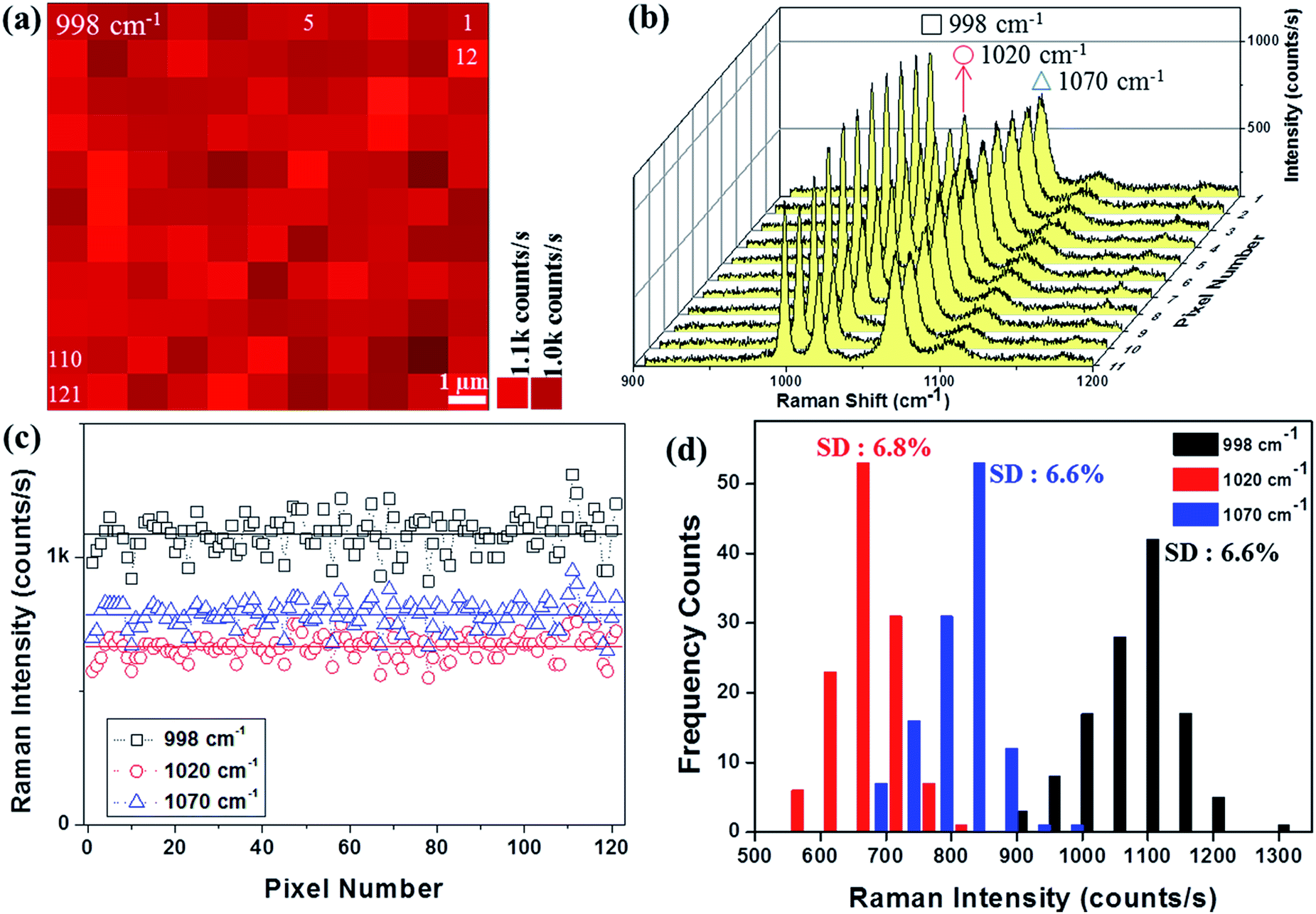 | ||
| Fig. 4 Raman signal uniformity of a 3D plasmonic nanostructure. (a) 2D Raman mapping of a BT-treated 3D plasmonic nanostructure. The Raman mapping was based on the signal intensity at 998 cm−1 Raman mode. The Raman mapping area was 11 × 11 μm2, and the illumination spot (0.58 μm2) was stepped in 1 μm steps. Some pixel number was denoted in the 2D map. (b) BT SERS spectra from the first row (pixels 1 to 11). (c) Variation of SERS intensity over the entire mapping area at the 998, 1020, and 1070 cm−1 Raman modes. Solid lines represent the mean value for each Raman mode. (d) Frequency counts and standard deviation of each Raman mode obtained from (c). | ||
Fig. 5 shows quantitative analysis of BT sensing on 3D plasmonic nanostructures. The SERS substrates were immersed in an 1 mL solution containing different BT concentrations (ranging from 2 μM to 20 pM) in ethanol solution for one hour. After removing from the BT solution, the SERS substrates were rinsed in ethanol several times and very gently blown dry with nitrogen gas. In Fig. 5a, SERS intensity of BT molecules changes proportionally with BT concentration. BT yields clear Raman bands at 415 cm−1, 998 cm−1, 1020 cm−1, 1070 cm−1, 1575 cm−1 and no fluorescence background signal was apparent. The 0.2 nM BT solution clearly yielded these five distinct characteristic peaks, indicating that the LOD of the SERS substrate was about 0.2 nM BT. A calibration plot with five known concentrations ranging from 2 μM to 0.2 nM was obtained with a good correlation coefficient of 0.99 (Fig. 5b). In the dipping method (case for BT), it's very difficult to quantify the number of adsorbed molecules contributing to the SERS signal and SERS substrates in some cases are dipped for many hours to increase the surface coverage. To get a precise quantitative data, we used a drop and dry method using non-volatile methylene blue (MB) molecules. 5 μL aqueous solutions containing different MB concentrations were dropped onto the SERS substrates, and then SERS substrates were dried for an hour. The wetted diameter was about 4 mm. The LOD value was measured to be 1.5 nM (ESI, Fig. S8†). Given the detection area measured using the 50× objective lens (1.5 μm in diameter), an 1.5 nM MB solution produces a SERS signal from 9.0 × 102 MB molecules within a single field of view.
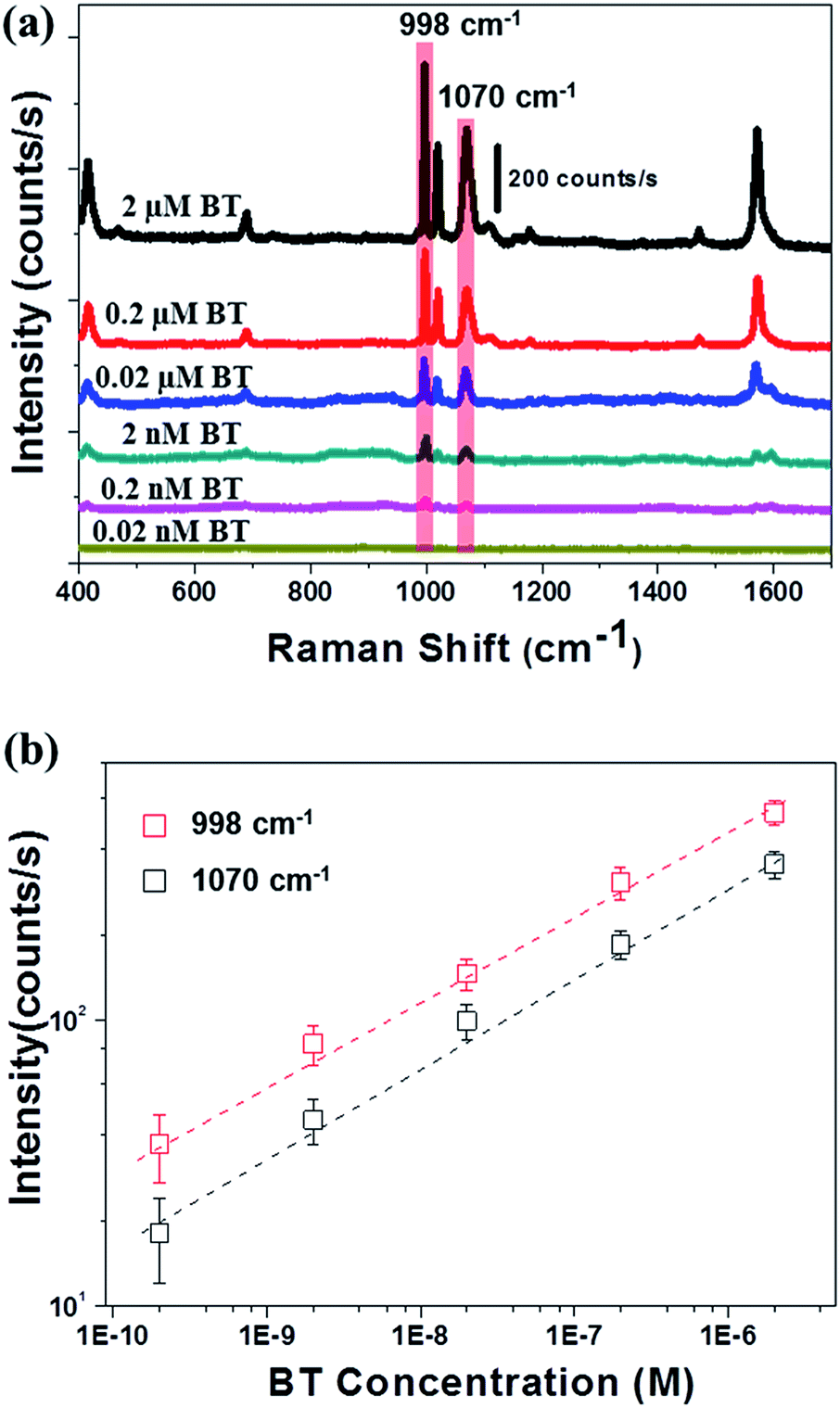 | ||
| Fig. 5 Quantitative data of BT sensing on 3D plasmonic nanostructures. (a) Comparison of the SERS spectra obtained from 2 μM to 20 pM BT-treated 3D plasmonic nanostructures. (b) Calibration plot with five known concentrations. The SERS intensities at 998 cm−1 and 1070 cm−1 were used for the calibration plot. The error bar shows the standard deviation of SERS intensities at 5 different locations. | ||
Conclusions
In summary, we developed highly efficient 3D plasmonic nanostructures with high areal density for SERS. The near-field enhancement of the 3D plasmonic nanostructures provided highly efficient optical responses across the full visible range, and highly sensitive and uniform SERS sensing capabilities. The 3D plasmonic nanostructures were fabricated using a simple maskless plasma treatment of the soft polymer surface and subsequent deposition of metal–dielectric–metal layers. The efficient and wavelength-tunable 3D plasmonic nanostructures have great potential for use in plasmon-mediated optical, energy and sensing applications.Experimental
Fabrication of the 3D plasmonic nanostructures
The PDMS used throughout the study was Sylgard 184 (Dow Corning Corp.). The elastomer was mixed in a 10![[thin space (1/6-em)]](https://www.rsc.org/images/entities/char_2009.gif) :1 ratio with its curing agent and then placed in a vacuum desiccator for 30 min to remove bubbles created during mixing. Samples were then prepared by pouring the PDMS solution into square Petri dishes, followed by curing at 90 °C overnight. Smooth PDMS pretreatment was performed by exposing the PDMS surface to a CF4 plasma in a custom-built radio frequency (RF) RIE system RIE (SNTEK, Co. Ltd) employing a 13.56 MHz capacitively coupled plasma supply. CF4 gas was introduced into the chamber at a flow rate of 5 standard cubic centimetres per minute (sccm), and the base pressure was kept constant at 8 × 10⁻² Torr while the RF power was maintained at 100 W in each experiment. PDMS nanoprotrusions were generated by the CF4 RIE. Ag nanostructures were directly grown on the PDMS protrusions using a thermal evaporation system (SNTEK, Co. Ltd) with a deposition rate of 2.2 Å s−1. A thin alumina spacer layer was formed on the Ag nanostructures at 100 °C using an ALD system [Lucida M100, NCD]. Trimethyl aluminum (TMA, Al2(CH3)6) and deionized water vapour were used as the aluminum precursor and oxygen source, respectively. The temperature of the TMA source was maintained at 10 °C using a cooling circulator. The canister containing the water source was maintained at room temperature. During deposition, argon gas was continuously flowed through the reaction chamber at a rate of 100 sccm. The growth rate was 1.4 Å per cycle, and 70 cycles resulted in the deposition of a 9.8 nm Al2O3 layer onto the Ag nanostructures. Finally, the top Ag NPs were deposited onto the alumina surfaces using a thermal evaporation system, which completed the 3D plasmonic nanostructures. The nominal thickness of the Ag was monitored using a quartz crystal oscillator.
:1 ratio with its curing agent and then placed in a vacuum desiccator for 30 min to remove bubbles created during mixing. Samples were then prepared by pouring the PDMS solution into square Petri dishes, followed by curing at 90 °C overnight. Smooth PDMS pretreatment was performed by exposing the PDMS surface to a CF4 plasma in a custom-built radio frequency (RF) RIE system RIE (SNTEK, Co. Ltd) employing a 13.56 MHz capacitively coupled plasma supply. CF4 gas was introduced into the chamber at a flow rate of 5 standard cubic centimetres per minute (sccm), and the base pressure was kept constant at 8 × 10⁻² Torr while the RF power was maintained at 100 W in each experiment. PDMS nanoprotrusions were generated by the CF4 RIE. Ag nanostructures were directly grown on the PDMS protrusions using a thermal evaporation system (SNTEK, Co. Ltd) with a deposition rate of 2.2 Å s−1. A thin alumina spacer layer was formed on the Ag nanostructures at 100 °C using an ALD system [Lucida M100, NCD]. Trimethyl aluminum (TMA, Al2(CH3)6) and deionized water vapour were used as the aluminum precursor and oxygen source, respectively. The temperature of the TMA source was maintained at 10 °C using a cooling circulator. The canister containing the water source was maintained at room temperature. During deposition, argon gas was continuously flowed through the reaction chamber at a rate of 100 sccm. The growth rate was 1.4 Å per cycle, and 70 cycles resulted in the deposition of a 9.8 nm Al2O3 layer onto the Ag nanostructures. Finally, the top Ag NPs were deposited onto the alumina surfaces using a thermal evaporation system, which completed the 3D plasmonic nanostructures. The nominal thickness of the Ag was monitored using a quartz crystal oscillator.
Measurements and characterizations
The reflectance spectra of the 3D plasmonic nanostructures were measured using spectrometers (Ocean Optics, USB4000) attached to an optical microscope (Nikon, L150) with a 10× objective lens. The reflected light from the 3D plasmonic nanostructure was collected through the same objective lens and analyzed by the spectrometer. The light reflected from the smooth silver mirror was measured as a reference. The normalized reflectance spectra of the plasmonic nanostructures are shown in Fig. 2b and c. The SERS measurements were performed by immersing the substrates in a solution containing 2 mM benzenethiol (BT) in ethanol for one hour. After removing from the BT solution, the SERS substrates were rinsed in ethanol several times and very gently blown dry with nitrogen gas. For quantitative measurement of BT, the SERS substrates were immersed in an 1 mL solution containing different BT concentrations (ranging from 2 μM to 20 pM) in ethanol solution for one hour. Since BT is highly volatile, the glass Petri-dish should be sealed during BT treatments. After removing from the Petri-dish, the SERS substrates were rinsed in ethanol several times and very gently blown dry with nitrogen gas. SERS measurements were collected using a Raman microscope (Horiba Jobin Yvon) equipped with a spectrometer and a thermoelectrically cooled charge coupled device (CCD). The excitation laser had a wavelength of λ = 632.8 nm and the power impinging upon the sample was 0.45 mW. A 50× objective lens with NA = 0.5 was used to focus the excitation laser onto the sample and collect the scattered Raman signals. The uniformity of the Raman signal was obtained from the BT-treated 3D plasmonic substrate. A 100× objective lens was used for the Raman mapping. The Raman mapping area was 11 × 11 μm2, and the beam was stepped in 1 μm steps. The surface morphologies were characterized by field emission scanning electron microscopy (FE-SEM; Jeol JSM-6700F). High-resolution cross-sectional image of the 3D plasmonic nanostructures were collected using field emission transmission electron microscopy (FE-TEM; Jeol JEM-2100 HR).FDTD simulation
The 3D plasmonic nanostructures were simplified in the simulations by assuming that the bottom Ag nanostructures formed spheres 60 nm in diameter. A 10 nm thick alumina film conformed to the bottom Ag nanostructures. Top Ag NPs were randomly distributed across the alumina surface and were modelled as hemispherical in shape. The Ag NP sizes and the nanogaps (less than 10 nm) between Ag NPs were held constant for all three plasmonic substrates (the 3D and 2D plasmonic nanostructures and the Ag NPs on the Si substrate). The linearly polarized 632.8 nm plane wave illumination beam were directed onto the 3D plasmonic nanostructure. The refractive index of alumina was set to 1.7659, and the dispersive and lossy nature of the silver was modelled using the auxiliary differential equation method applied to the Drude model. The unit pixels were 0.83 nm in size. The SERS enhancements from the three plasmonic substrates were compared by measuring the surface averaged values of |E|4/|E0|4, where |E0| and |E| are the incident and local electric field intensity. The average value of |E|4/|E0|4 for the 3D plasmonic nanostructure was obtained from the values measured across 642 pixels, whereas 450 pixels are used to calculate the value on the 2D plasmonic nanostructure and Ag NPs on the Si substrate.Acknowledgements
This study was supported financially by the Fundamental Research Program (PNK5060) of the Korean Institute of Materials Science (KIMS). Dr S.-G. Park is grateful for support from the Basic Science Research Program of the National Research Foundation of Korea (NRF) funded by the Ministry of Science, ICT and Future Planning (NRF-2015R1C1A01053884).Notes and references
- H. Atwater and A. Polman, Nat. Mater., 2010, 9, 205–213 CrossRef CAS PubMed.
- J. S. Clausen, E. Højlund-Nielsen, A. B. Christiansen, S. Yazdi, M. Grajower, H. Taha, U. Levy, A. Kristensen and N. A. Mortensen, Nano Lett., 2014, 14, 4499–4504 CrossRef CAS PubMed.
- T. Y. Jeon, S.-G. Park, D.-H. Kim and S.-H. Kim, Adv. Funct. Mater., 2015, 25, 4681–4688 CrossRef CAS.
- G. Konstantatos and E. H. Sargent, Nat. Nanotechnol., 2010, 5, 391–400 CrossRef CAS PubMed.
- J. Lee, S. Mubeen, X. Ji, G. D. Stucky and M. Moskovits, Nano Lett., 2012, 12, 5014–5019 CrossRef CAS PubMed.
- S. C. Warren and E. Thimsen, Energy Environ. Sci., 2012, 5, 5133–5146 CAS.
- M.-K. Kwon, J.-Y. Kim, B.-H. Kim, I.-K. Park, C.-Y. Cho, C. C. Byeon and S.-J. Park, Adv. Mater., 2008, 20, 1253–1257 CrossRef CAS.
- J.-B. Kim, J.-H. Lee, C.-K. Moon, S.-Y. Kim and J.-J. Kim, Adv. Mater., 2013, 25, 3571–3577 CrossRef CAS PubMed.
- A. Tittl, P. Mai, R. Taubert, D. Dregely, N. Liu and H. Giessen, Nano Lett., 2011, 11, 4366–4369 CrossRef CAS PubMed.
- N. Liu, M. Mesch, T. Weiss, M. Hentschel and H. Giessen, Nano Lett., 2010, 10, 2342–2348 CrossRef CAS PubMed.
- J. a Schuller, E. S. Barnard, W. Cai, Y. C. Jun, J. S. White and M. L. Brongersma, Nat. Mater., 2010, 9, 193–204 CrossRef CAS PubMed.
- A. Moreau, C. Ciracì, J. J. Mock, R. T. Hill, Q. Wang, B. J. Wiley, A. Chilkoti and D. R. Smith, Nature, 2012, 492, 86–89 CrossRef CAS PubMed.
- D. Wang, W. Zhu, M. D. Best, J. P. Camden and K. B. Crozier, Sci. Rep., 2013, 3, 2867 Search PubMed.
- C. Ciracì, X. Chen, J. J. Mock, F. McGuire, X. Liu, S.-H. Oh and D. R. Smith, Appl. Phys. Lett., 2014, 104, 023109 CrossRef.
- S. Ayas, G. Cinar, A. D. Ozkan, Z. Soran, O. Ekiz, D. Kocaay, A. Tomak, P. Toren, Y. Kaya, I. Tunc, H. Zareie, T. Tekinay, A. B. Tekinay, M. O. Guler and A. Dana, Sci. Rep., 2013, 3, 2624 Search PubMed.
- R. Fernández-García, Y. Sonnefraud, A. I. Fernández-Domínguez, V. Giannini and S. a. Maier, Contemp. Phys., 2014, 55, 1–11 CrossRef.
- N. U. L. Raman, M. S. Schmidt, A. Boisen, J. Ju and Q. Lin, ACS Nano, 2013, 7, 5350–5359 CrossRef PubMed.
- M. S. Schmidt, J. Hübner and A. Boisen, Adv. Mater., 2012, 24, OP11–18 CAS.
- S.-G. Park, S.-K. Lee, J. H. Moon and S.-M. Yang, Lab Chip, 2009, 9, 3144–3150 RSC.
- S.-K. Lee, S.-G. Park, J. H. Moon and S.-M. Yang, Lab Chip, 2008, 8, 388–391 RSC.
- Y. Xia and G. M. Whitesides, Annu. Rev. Mater. Sci., 1998, 28, 153–184 CrossRef CAS.
- M. Scharrer, X. Wu, a. Yamilov, H. Cao and R. P. H. Chang, Appl. Phys. Lett., 2005, 86, 151113 CrossRef.
- S.-G. Park, T. Y. Jeon, H. C. Jeon, S.-M. Yang, J.-D. Kwon, C.-W. Mun, B. Cho, C. S. Kim and D.-H. Kim, J. Mater. Chem. C, 2014, 2, 1957 RSC.
- W.-D. Li, F. Ding, J. Hu and S. Y. Chou, Opt. Express, 2011, 19, 3925–3936 CrossRef PubMed.
- F. S. Ou, M. Hu, I. Naumov, A. Kim, W. Wu, A. M. Bratkovsky, X. Li, R. S. Williams and Z. Li, Nano Lett., 2011, 11, 2538–2542 CrossRef CAS PubMed.
- M. Hu, F. S. Ou, W. Wu, I. Naumov, X. Li, A. M. Bratkovsky, R. S. Williams and Z. Li, J. Am. Chem. Soc., 2010, 132, 12820–12822 CrossRef CAS PubMed.
- A. V Whitney, J. W. Elam, S. Zou, A. V Zinovev, P. C. Stair, G. C. Schatz and R. P. Van Duyne, J. Phys. Chem. B, 2005, 109, 20522–20528 CrossRef PubMed.
- X. Zhang, J. Zhao, A. V Whitney, J. W. Elam and R. P. Van Duyne, J. Am. Chem. Soc., 2006, 128, 10304–10309 CrossRef CAS PubMed.
- C. T. Campbell, Surf. Sci. Rep., 1997, 27, 1–111 CrossRef CAS.
- S.-G. Park, C. Mun, M. Lee, T. Y. Jeon, H.-S. Shim, Y.-J. Lee, J.-D. Kwon, C. S. Kim and D.-H. Kim, Adv. Mater., 2015, 27, 4290–4295 CrossRef CAS PubMed.
- E. Prodan, C. Radloff, N. J. Halas and P. Nordlander, Science, 2003, 302, 419–422 CrossRef CAS PubMed.
- C. L. R. Eric and P. G. Etchegoin, Principles of surface-enhanced Raman spectroscopy, 2009 Search PubMed.
- A. D. McFarland, M. A. Young, J. A. Dieringer and R. P. Van Duyne, J. Phys. Chem. B, 2005, 109, 11279–11285 CrossRef CAS PubMed.
- K. a Willets and R. P. Van Duyne, Annu. Rev. Phys. Chem., 2007, 58, 267–297 CrossRef CAS PubMed.
- H.-Y. Chen, M.-H. Lin, C.-Y. Wang, Y.-M. Chang and S. Gwo, J. Am. Chem. Soc., 2015, 137, 13698–13705 CrossRef CAS PubMed.
Footnotes |
| † Electronic supplementary information (ESI) available: SEM images of Ag nanostructures, and comparison of the SERS performance measured at the 3D and 2D plasmonic nanostructures. See DOI: 10.1039/c6ra28150h |
| ‡ M. K. Lee and T. Y. Jeon contributed equally to this project. |
| This journal is © The Royal Society of Chemistry 2017 |