DOI:
10.1039/C6RA26823D
(Paper)
RSC Adv., 2017,
7, 4444-4452
Band-tunable photodetectors based on graphene/alloyed ZnxCd1−xS film hybrids
Received
15th November 2016
, Accepted 22nd December 2016
First published on 16th January 2017
Abstract
Graphene/semiconductor film hybrid-based photodetectors have attracted extensive attention because of their ultra-high performance. However, only the photoconductive behavior of binary semiconductors with fixed bandgap was studied since achieving tunable optoelectronic properties is significant for the practical applications of semiconductors. Herein, alloyed ZnxCd1−xS (0 ≤ x ≤ 1) films with complete compositional tunability were successfully prepared by an e-beam evaporation method via changing the molar ratio of ZnS to CdS in the target. UV-visible optical absorption measurements showed that the composition-dependent band-edge absorption is generated in the as-prepared alloyed ZnxCd1−xS films, with the energy gaps continuously shifted from 2.41 eV (x = 0, CdS) to 3.67 eV (x = 1, ZnS). After graphene is transferred on the alloyed ZnxCd1−xS films, band-tunable photodetectors are achieved based on graphene/alloyed ZnxCd1−xS film hybrids with the cut-off wavelength in the spectral response gradually changing from 410 nm to 580 nm. Obviously, the method introduced in this study can be extended to fabricate other graphene/alloyed ternary film hybrid-based photodetectors with band tunability in the visible and infrared region.
1. Introduction
Photodetectors have attracted significant attention in recent years owing to their various applications in the fields such as communication, sensing, environmental protection, and imaging.1–3 In terms of the dimensionality of photoactive material, these mainly include one-dimensional (1D) nanostructure-based and film-based photodetectors.4–6 The film-based photodetectors possess a low performance due to the low carrier mobility of the film consisting of nanocrystals. Our previous studies and studies reported by other group have shown that the performance can be greatly enhanced by hybridizing semiconductor films with graphene, a two-dimensional single-layer of sp2 bonded carbon atoms with ultra-high carrier mobility,7–17 which can provide an ultra-fast transport channel for the photogenerated carriers of photoactive materials. Konstantatos et al. demonstrated a responsivity of 107 A W−1 in a photodetector based on graphene/PbS quantum dot hybrids.9 This remarkable performance clearly shows the superiority of this approach. It is well known that for photoconductive devices, the detected light wavelength depends on the band gap of a photoactive semiconductor. Among these, only the photoconductive behavior of binary semiconductors with a fixed bandgap was studied. However, achieving tunable optoelectronic properties is significant for the practical applications of semiconductors. Therefore, it is desirable to achieve band-tunable graphene/semiconductor film hybrid-based photodetectors.
Alloying of binary semiconductors is an important approach to achieve tunable optoelectronic properties via composition modulation. Our previous study illustrates that Eg(ABxC1−x) (the energy gap of the alloyed ABxC1−x) can be continuously tuned from Eg(AB) (the energy gap of the binary compound AB) to Eg(AC) (the energy gap of the binary compound AC) as the composition x varies.18 This approach has been widely utilized to obtain tunable optoelectronic properties including photoluminescence, lasing, and photocatalysis.18–25 However, only few studies have reported nanowire-based band-tunable photodetectors based on the abovementioned bandgap engineering.26–28 To the best of our knowledge, graphene/semiconductor film hybrid-based photodetectors with band tunability have never been reported.
In view of the tunable photoconductive properties of graphene/alloyed film hybrids, ternary ZnxCd1−xS (0 ≤ x ≤ 1) is a good candidate. As a wide-gap II–VI semiconductor, ZnS and CdS have a bandgap of 3.67 eV and 2.41 eV, respectively, which implies that ZnS and CdS are potentially excellent photoactive materials for photodetectors. Several studies have investigated the photocatalytic activity and photoelectrochemical performance of the graphene/ZnxCd1−xS hybrids.29–31 In this study, we prepared alloyed wide bandgap ZnxCd1−xS (0 ≤ x ≤ 1) films by e-beam evaporation method by changing the molar ratio of ZnS to CdS in the target, and for the first time, examined the band-tunable photoconductive properties of graphene/alloyed ZnxCd1−xS film hybrids.
2. Experimental
2.1. Preparation of the ZnxCd1−xS film
ZnS (99.99% purity) and CdS (99.99% purity) powders with different molar ratios were mixed and ground in a grinding dish for 30 minutes. After this, the mixed powders were sintered at 950 °C for 1.5 hours with 10 sccm H2 and 20 sccm Ar. With the sintered ZnxCd1−xS powders as targets, the ZnxCd1−xS film with a thickness of 60 nm was deposited on a 300 nm SiO2/Si substrate by e-beam evaporation. The vacuum remained at 2 × 10⁻⁴ Pa during the entire deposition process. Before the graphene transfer, the ZnxCd1−xS film on the Si/SiO2 substrate was annealed for 30 min at 300 °C under low pressure with 10 sccm H2 and 20 sccm Ar, enabling the film adhesion to the substrate as it was placed in water to pick up the graphene films.
2.2. Graphene growth and transfer
The details of graphene growth and transfer can be found in our previous studies,32,33 except that the PMMA carrier for graphene transfer was removed by annealing for 2 hours at 400 °C under low pressure with 10 sccm H2 and 20 sccm Ar. This method enables the crackless transfer of graphene.17,34
2.3. Transistor fabrication
After PMMA was removed, devices with a channel length of 20 μm and width of 500 μm were fabricated with a shadow mask. The doped Si substrate served as a global back gate. Cr/Au (10 nm/100 nm) was used as the electrical contact metal for the source and drain electrodes were deposited using a high-vacuum thermal evaporation system.
2.4. Characterization and measurement
The composition of ZnxCd1−xS films was characterized via energy dispersive X-ray spectroscopy (EDX) using a Hitachi SU8020 scanning electron microscope and via X-ray photoelectron spectroscopy (XPS) (ESCALAB250Xi). XRD patterns of the samples were obtained using an X-ray diffractometer (X'Pert Pro MPD) with λ = 1.54056 Å. UV-vis absorption (UV-3600) was conducted on the samples after they were transferred on a quartz substrate. The microstructure of ZnxCd1−xS was characterized by transmission electron microscopy (TEM) (Tecnai G2 F20). The electrical and photoconductive properties of the graphene/CdS film and graphene/ZnxCd1−xS film hybrid devices were measured by a semiconductor parameter analyzer system (Keithley 2636B) at room temperature using light emitting diodes with the corresponding wavelength as the incident light.
3. Results and discussion
3.1. Surface information and composition
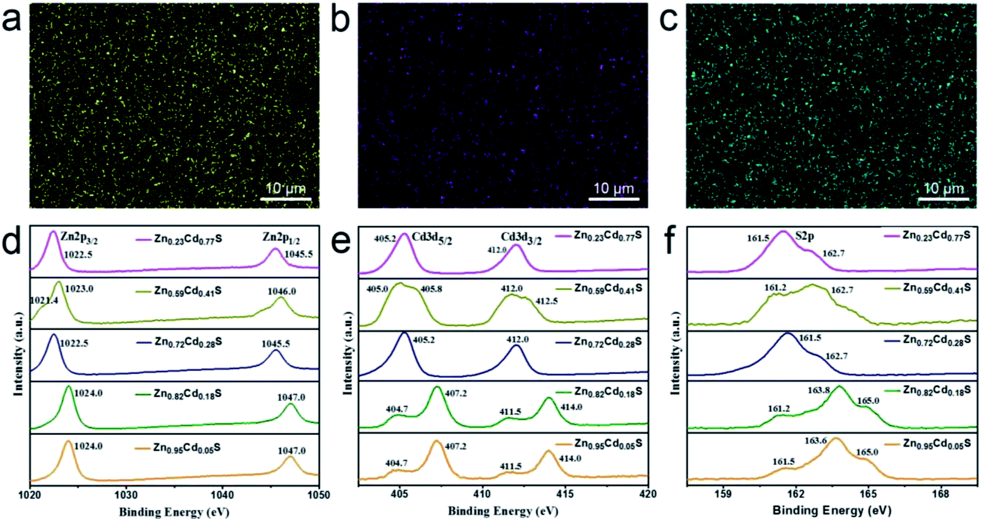
To investigate the surface information and determine the composition x of the as-deposited ternary ZnxCd1−xS films, EDX mapping and XPS analysis was carried out. The uniform distribution of Zn, Cd, and S in the EDX mapping shows that the as-deposited film is ZnxCd1−xS (Fig. 1a–c). Fig. 1d–f show the XPS survey spectra of the alloyed ZnxCd1−xS films obtained by e-beam evaporation with the targets having various ZnS/CdS molar ratios of 2![[thin space (1/6-em)]](https://www.rsc.org/images/entities/char_2009.gif) :8, 5:5, 7:3, 8:2, and 9:1. The XPS peaks of Zn 2p3/2, Zn 2p1/2, Cd 3d5/2, Cd 3d3/2, and S 2p for the alloyed ZnxCd1−xS films are located at around 1022.5 eV, 1045.5 eV, 405.2 eV, 412.0 eV, and 162.7 eV, respectively, which are all in agreement with the corresponding binding energies of ZnxCd1−xS;25,35,36 it provides a solid evidence that the as-deposited product is ZnxCd1−xS. The radii of the Zn2+ ions (0.74 Å) are smaller than those of the Cd2+ ions (0.97 Å), leading to shorter bond lengths of Zn–S than those of Cd–S. The local environment around Cd2+ ions would be changed due to the substitution of Zn2+ ions in place of Cd2+ ions in the CdS lattice. Therefore, the variation of the coordination environments around the S2− ions would affect the position of the binding energy of S 2p, leading to a shift of the binding energy to high values as the number of Zn2+ ions increases. The area under the peaks was calibrated to obtain the Zn/Cd ratio, namely composition (x) values. The compositions of the ternary ZnxCd1−xS films obtained by e-beam evaporation with the targets having various ZnS/CdS molar ratios of 2:8, 5:5, 7:3, 8:2, and 9:1 were calculated to be x = 0.23, 0.59, 0.72, 0.82, and 0.95, respectively, as shown in Table 1.
:8, 5:5, 7:3, 8:2, and 9:1. The XPS peaks of Zn 2p3/2, Zn 2p1/2, Cd 3d5/2, Cd 3d3/2, and S 2p for the alloyed ZnxCd1−xS films are located at around 1022.5 eV, 1045.5 eV, 405.2 eV, 412.0 eV, and 162.7 eV, respectively, which are all in agreement with the corresponding binding energies of ZnxCd1−xS;25,35,36 it provides a solid evidence that the as-deposited product is ZnxCd1−xS. The radii of the Zn2+ ions (0.74 Å) are smaller than those of the Cd2+ ions (0.97 Å), leading to shorter bond lengths of Zn–S than those of Cd–S. The local environment around Cd2+ ions would be changed due to the substitution of Zn2+ ions in place of Cd2+ ions in the CdS lattice. Therefore, the variation of the coordination environments around the S2− ions would affect the position of the binding energy of S 2p, leading to a shift of the binding energy to high values as the number of Zn2+ ions increases. The area under the peaks was calibrated to obtain the Zn/Cd ratio, namely composition (x) values. The compositions of the ternary ZnxCd1−xS films obtained by e-beam evaporation with the targets having various ZnS/CdS molar ratios of 2:8, 5:5, 7:3, 8:2, and 9:1 were calculated to be x = 0.23, 0.59, 0.72, 0.82, and 0.95, respectively, as shown in Table 1.
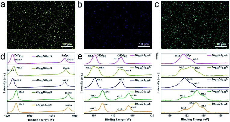 |
| | Fig. 1 EDX mapping of (a) Zn, (b) Cd, and (c) S conducted on the as-deposited ZnxCd1−xS films on 300 nm SiO2/Si substrate. XPS spectra of the as-deposited ZnxCd1−xS films with different compositions: (d) Zn 2p3/2 and Zn 2p1/2, (e) Cd 3d5/2 and Cd 3d3/2, and (f) S 2p. It provides solid evidence that the as-deposited product is a ZnxCd1−xS film. | |
Table 1 The XPS characteristic peaks of Zn 2p and Cd 3d are used for the composition estimation. The compositions of ternary ZnxCd1−xS films obtained by e-beam evaporation with the targets having various ZnS/CdS molar ratios of 2:8, 5:5, 7:3, 8:2, and 9:1 are calculated to be x = 0.23, 0.59, 0.72, 0.82, and 0.95, respectively, by calibrating the area under the XPS peaks of Zn 2p and Cd 3d
| Molar ratio of ZnS/CdS |
Atomic percentage% |
Film composition |
| Zn 2p |
Cd 3d |
S 2p |
| 2/8 |
11.35 |
39.51 |
49.15 |
Zn0.23Cd0.77S |
| 5/5 |
13.87 |
9.58 |
21.25 |
Zn0.59Cd0.41S |
| 7/3 |
37.77 |
14.8 |
47.42 |
Zn0.72Cd0.28S |
| 8/2 |
27.54 |
6.09 |
28.99 |
Zn0.82Cd0.18S |
| 9/1 |
30.62 |
1.70 |
28.30 |
Zn0.95Cd0.05S |
3.2. Crystallinity and microstructure
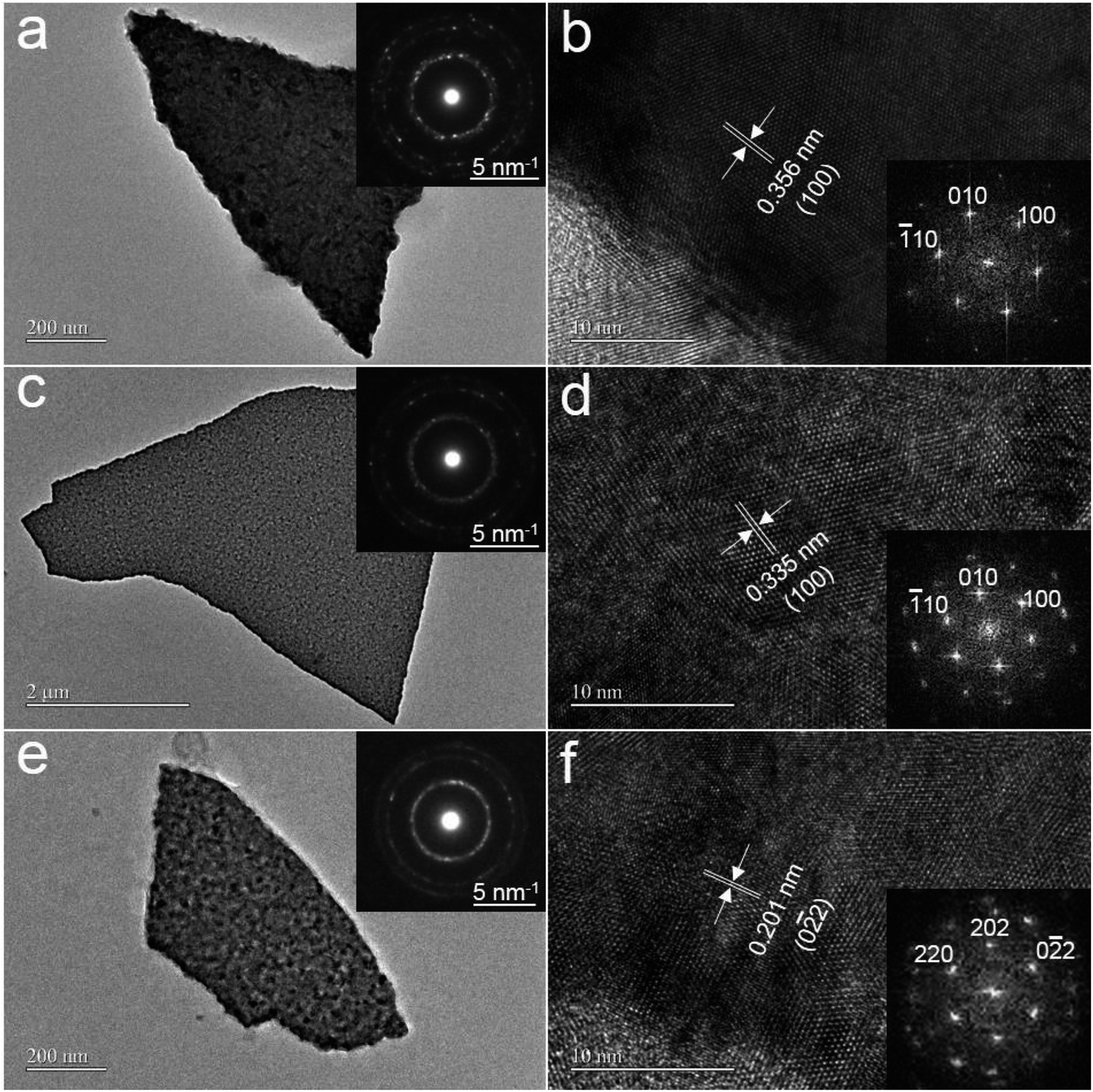
The crystallinity and microstructure of ZnxCd1−xS films were characterized by TEM. The TEM images in Fig. 2a, c, and e show the film morphology after the deposited ZnxCd1−xS films on 300 nm SiO2/Si substrate were dispersed in ethanol. The selected-area electron-diffraction (SAED) patterns (insets in Fig. 2a, c, and e) confirm that the as-deposited films are polycrystalline. Combining the high-resolution TEM (HRTEM) images with the corresponding Fourier transform images in Fig. 2b, d, and f, the as-deposited ZnxCd1−xS films with x = 0.23 and 0.59 are characterized to have the hexagonal wurtzite structure, whereas ZnxCd1−xS films with x = 0.82 have the zinc blende structure. This phenomenon that the structure of the alloys is related to the composition was also reported by an other group.21 Furthermore, the interplanar distances of {100} for hexagonal ZnxCd1−xS with x = 0.23 and 0.59 are 3.56 Å and 3.35 Å, respectively, confirming that the interplanar distances of ZnxCd1−xS films vary with the composition x.
 |
| | Fig. 2 TEM images of the as-deposited ZnxCd1−xS films with (a) x = 0.23, (c) x = 0.59, and (e) x = 0.82. The inset is the corresponding SAED. HRTEM images of the ZnxCd1−xS films with (b) x = 0.23, (d) x = 0.59, and (f) x = 0.82. The corresponding Fourier transform images (inset) show that Zn0.23Cd0.77S and Zn0.59Cd0.41S have a hexagonal wurtzite structure, whereas Zn0.82Cd0.18S has a zinc blende structure. The interplanar distances of {100} for hexagonal Zn0.23Cd0.77S and Zn0.59Cd0.41S are 3.56 Å and 3.35 Å, respectively, confirming that the interplanar distances of ZnxCd1−xS films vary with the composition x. | |
3.3. Crystal structure
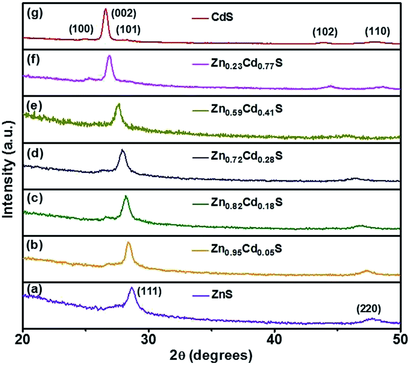
The X-ray diffraction (XRD) measurements were further conducted to investigate the structure of all ZnxCd1−xS samples with different x values, as shown in Fig. 3. Curves (a) and (g) are for the pure ZnS and CdS films, respectively, which correspond to the respective bulk zinc blende ZnS (JCPDS 77-2100) and wurtzite CdS (JCPDS 70-2553) crystals. Curves (b)–(f) are for the samples obtained by e-beam evaporation with the targets having various ZnS to CdS molar ratios of 9:1, 8:2, 7:3, 5:5, and 2:8, respectively. The XRD patterns revealed that the ternary ZnxCd1−xS films over the compositions of x = 0.95, 0.82, and 0.72 have the zinc blende structure, whereas the ternary films with the composition of x = 0.59 and 0.23 have the wurtzite structure. It can be observed that the XRD peaks of zinc blende structured and wurtzite structured ZnxCd1−xS ternary films continuously shift to smaller angles from curves (a) to (d) and from curves (e) to (g), respectively, indicating that the lattice parameters of the films increase with of the decreasing composition x. The continuous peak shift further indicates that alloyed ZnxCd1−xS films with modulated compositions between ZnS and CdS were successfully achieved by an e-beam evaporation method via changing the molar ratio of ZnS to CdS in the target, which may also rule out the phase separation of ZnS or CdS.37,38
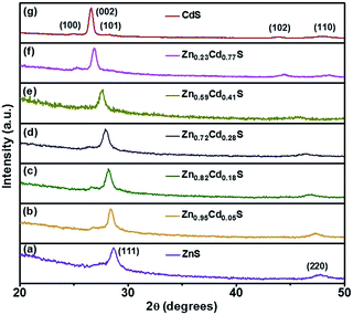 |
| | Fig. 3 XRD pattern of the ZnxCd1−xS films with different values of x. The XRD patterns show that the ternary ZnxCd1−xS films over compositions of x = 1, 0.95, 0.82, and 0.72 have a zinc blende structure, whereas the ternary films with composition of x = 0.59, 0.23, and 0 have a wurtzite structure. The continuous peak shifting indicates that alloyed ZnxCd1−xS films with modulated compositions between ZnS and CdS were successfully achieved. | |
3.4. Energy gap
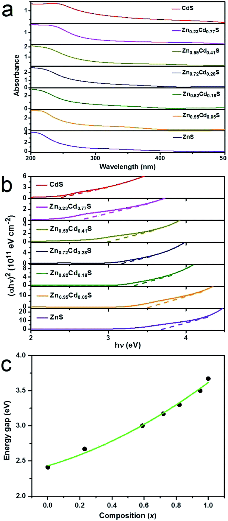
The UV-visible optical absorption spectra were acquired at room temperature to obtain the variation of light absorption for ZnxCd1−xS films with different values of x, as shown in Fig. 4a. The spectra clearly show that the absorption edge is gradually shifted towards a longer wavelength with the decreasing value of x. As is known, the optical absorption is related to the electron excitation from the valance band to the conduction band. Therefore, the shift towards a longer wavelength indicates a decrease in the energy gap (Eg). Moreover, Eg can be attained by extrapolating the straight line plot of (αhν)2 versus (hν) to the energy axis. The absorption coefficient (α) and the incident photon energy hν are related by the following equation:39,40where A is a constant, Eg is the band gap of the material, and the exponent n = 1/2 for the material with direct band gap. The variation of (αhν)2 as a function of hν is shown in Fig. 4b. Obviously, the obtained Eg of ZnxCd1−xS films with different values of x continuously decreases with the decreasing value of x.
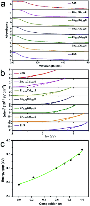 |
| | Fig. 4 (a) UV-visible optical absorption spectra of the ZnxCd1−xS films with different composition x on a quartz substrate. (b) The variation of (αhν)2 as function of hν for the ZnxCd1−xS films with different composition x. Eg can be attained by extrapolating the straight line plot of (αhν)2 versus (hν) to the energy axis. (c) Eg of the alloyed ZnxCd1−xS films as a function of the composition x. It can be seen that the variation of Eg with composition x slightly deviates from linear dependence, displaying downward bowing. | |
Eg of the alloyed ZnxCd1−xS films are plotted in Fig. 4c as a function of the composition x. It can be seen that the variation of Eg with composition x slightly deviates from linear dependence, displaying a downward bowing. This character has also been reported for many alloyed films,41–43 alloyed nanocrystals,44 and alloyed 1D nanostructures.19,21 In the case of the ZnxCd1−xS system, the nonlinear variation of Eg can be represented as a quadratic function of the composition x:19,45,46
| | |
Eg(x) = xEg(ZnS) + (1 − x)Eg(CdS) − x(1 − x)b
| (2) |
where
Eg(
x) is the energy gap of Zn
xCd
1−xS,
Eg(ZnS) is the energy gap of ZnS,
Eg(CdS) is the energy gap of CdS, and
b is the bowing parameter. The second-order polynomial fitting of the experimental results, as shown in
Fig. 4c (solid line), gives the following quadratic expression:
| | |
Eg(x) = 2.43 + 0.68x + 0.50x2
| (3) |
which yields the bowing parameter of
b = 0.50 eV. The obtained bowing parameter is similar to the value reported in the previous studies on Zn
xCd
1−xS.
19,42,43 Note that the slight variation of energy gaps resulted from different crystal structure (zinc blende or wurtzite) of alloyed Zn
xCd
1−xS films is ignored.
3.5. Photoconductive properties
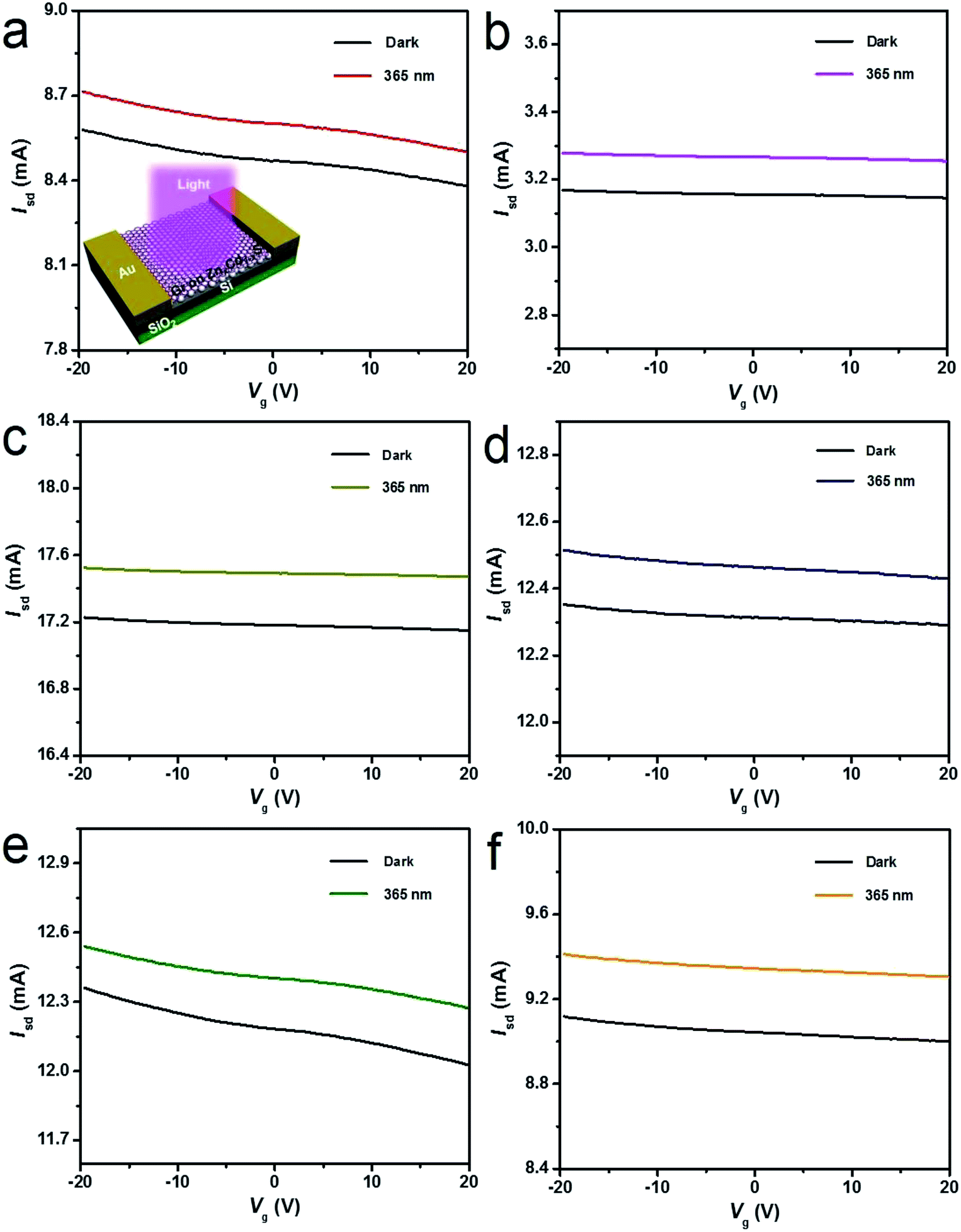
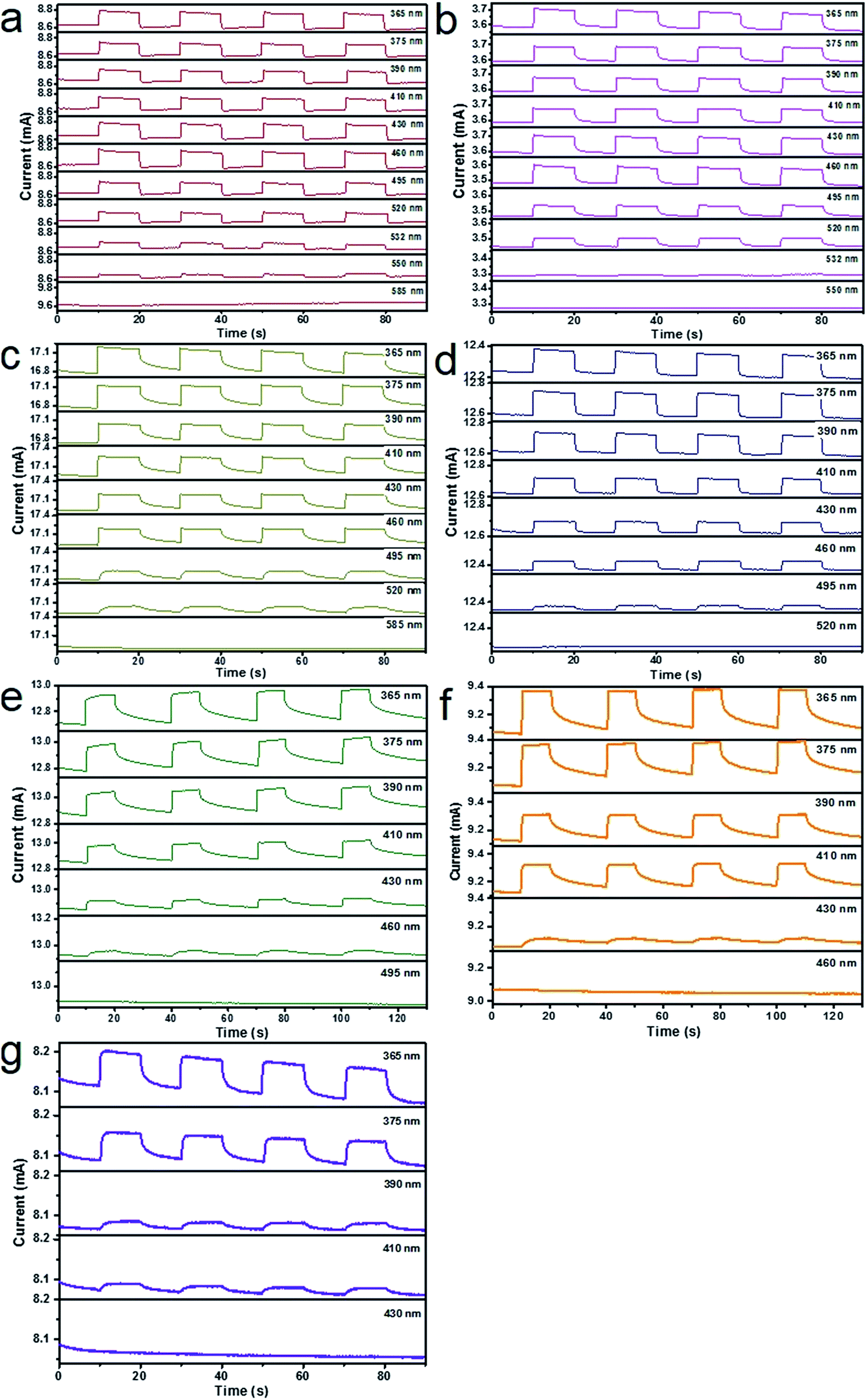
After graphene films are transferred on the alloyed ZnxCd1−xS films on the 300 nm SiO2/Si substrate, band-tunable photodetectors based on graphene/alloyed ZnxCd1−xS film hybrids can be achieved. To fabricate graphene/alloyed ZnxCd1−xS film-based field effect transistors, Cr/Au (10 nm/100 nm) electrodes with a length of 20 μm and width of 500 μm were deposited by e-beam evaporation through a shadow mask. After light was focused on the channel, the photoconductive properties of graphene/ZnxCd1−xS film hybrids could be investigated, schematically shown in the inset of Fig. 5a. Typical transfer characteristics of the back-gated transistors for graphene transferred on the ZnxCd1−xS films show a hole-dominated transport without the appearance of a Dirac point. This probably arises from the p-doping of oxygen in air.9,14,32 Upon 365 nm light irradiation, the source-drain current (Isd) obviously increases regardless of the gate bias (Vg) for all ZnxCd1−xS films with different compositions (Fig. 5). The increase in the hole-dominated current in the graphene channel means that the holes transfer from the ZnxCd1−xS film to graphene.9,14,15 Therefore, the working mechanism for a graphene/ZnxCd1−xS film hybrid photodetector is the same as that for a graphene/ZnS film hybrid photodetector, which was illustrated in a previous study.17 Fig. 6 depicts a time-dependent response of graphene/alloyed ZnxCd1−xS film hybrid-based device by switching light illumination with different wavelength yet at the same power of 1 mW cm−2 on and off periodically at a fixed voltage of 1.0 V. The current increases to a stable value of certain mA upon illumination, and then decreases to the initial value when the light is turned off, which shows good stability for the devices based on graphene/alloyed ZnxCd1−xS film hybrids. The responsivity and response time of the graphene/II–VI semiconductor film-based photodetectors can be observed in a previous study,17 and we only focus on the band tunability of the devices based on graphene/alloyed ZnxCd1−xS film hybrids in this study. All the photodetectors show that the photocurrents depend on the incident wavelength, with the largest values for the detectors with all values of x being located at around 365 nm (Fig. 6). In addition, the values of the largest photocurrent for the ternary ZnxCd1−xS (0 < x < 1) films are all higher than those of the binary compound CdS (x = 0) and ZnS (x = 1) films. Ren et al. also reported a similar phenomenon that the largest photocurrents of the ternary InAsxP1−x (0 < x < 1) nanowires are larger than those of the InP (x = 0) and InAs (x = 1) nanowires.28
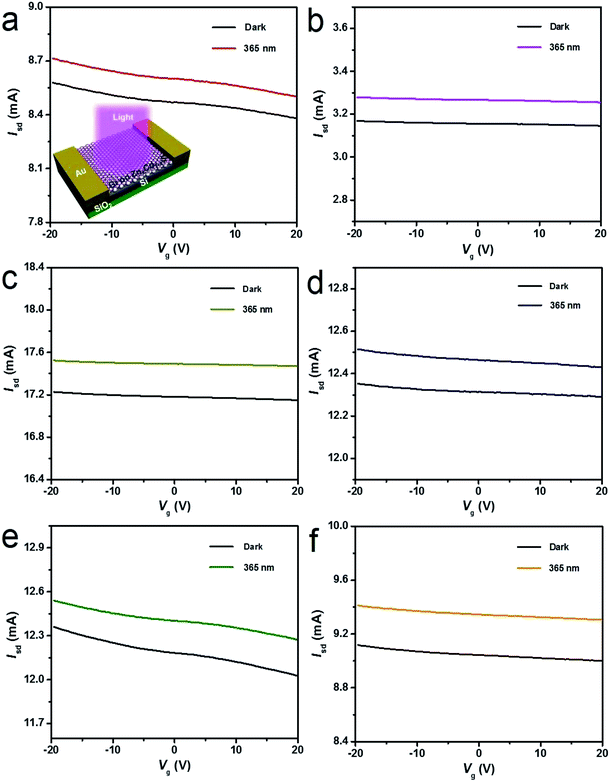 |
| | Fig. 5 Typical transfer characteristics of the back-gated transistors for graphene transferred on ZnxCd1−xS films with compositions (a) x = 0, (b) x = 0.23, (c) x = 0.59, (d) x = 0.72, (e) x = 0.82, and (f) x = 0.95, showing a hole-dominated transport. The inset shows the scheme of graphene/ZnxCd1−xS film hybrid-based photodetector. Upon 365 nm light irradiation, Isd obviously increases regardless of Vg for all ZnxCd1−xS films with different compositions. | |
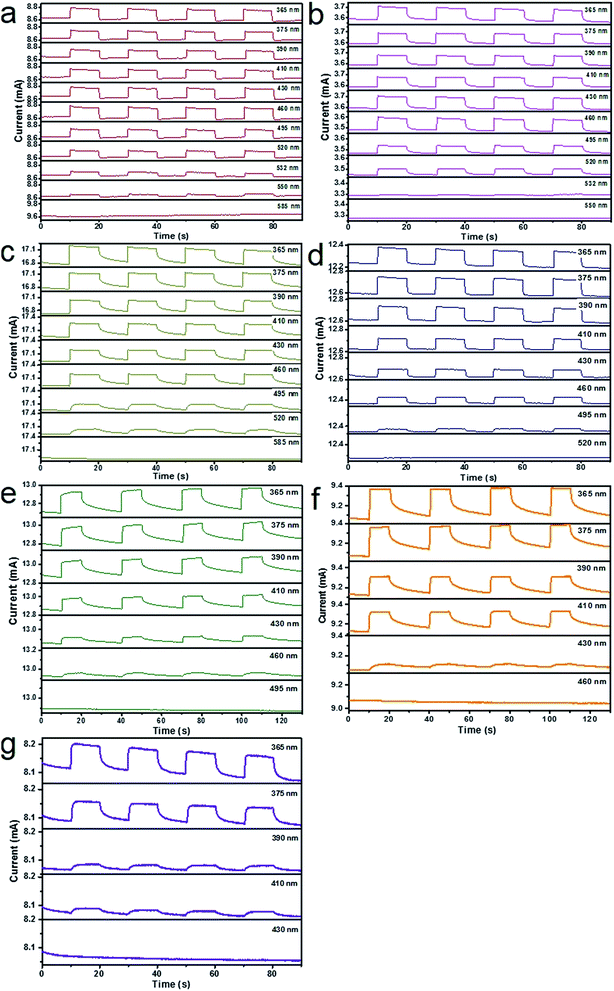 |
| | Fig. 6 Time-dependent response of graphene/alloyed ZnxCd1−xS film hybrid-based photodetectors with compositions (a) x = 0, (b) x = 0.23, (c) x = 0.59, (d) x = 0.72, (e) x = 0.82, (f) x = 0.95, and (g) x = 1, by switching light illumination with different wavelengths but the same power of 1 mW cm−2 on and off periodically at a fixed voltage of 1.0 V. All the photodetectors show that the photocurrents depend on the incident wavelength, with the largest values for the detectors with all values of x being located at around 365 nm. | |
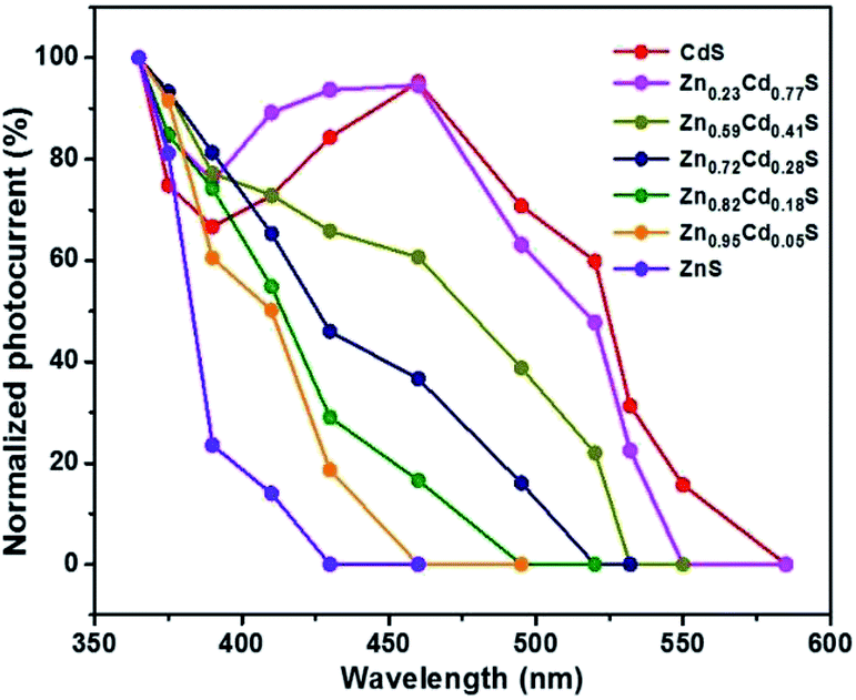
To attain the detailed wavelength related spectral response for the photodetector based on graphene/alloyed ZnxCd1−xS films, wavelength-dependent photocurrents of the devices were measured with the incident light wavelength scanned from 365 to 585 nm under a bias voltage of 1 V and a light intensity of 1 mW cm−2, as shown in Fig. 7. Note that the photocurrents calculated from the detectors based on graphene/alloyed ZnxCd1−xS films with different compositions are normalized. Two types of variation tendency of the spectral response for graphene/alloyed ZnxCd1−xS film hybrids are clearly observed. For graphene/ZnxCd1−xS film with compositions x = 1, 0.95, 0.82, and 0.72, the photocurrent increased with the decreasing excited wavelength, which is in good agreement with the results of the ZnS-based photodetector.5 However, for graphene/ZnxCd1−xS film with compositions x = 0.59, 0.23, and 0, the photocurrent increased with the decreasing excited wavelength as the wavelength is shorter than the value corresponding to the energy gap, and then decreased with the decreasing wavelength, and finally increased with the decreasing wavelength, namely presenting a peak and a valley. The different variation tendency of the spectral response was attributed to the different absorption behavior of the ZnxCd1−xS film with different compositions. For ZnxCd1−xS film with composition x = 0.59, 0.23, and 0, there is an obvious peak locating at hν around the corresponding energy gap of ZnxCd1−xS, whereas for ZnxCd1−xS film with a composition x = 1, 0.95, 0.82, and 0.72, the peak does not appear obvious (Fig. 4b). Choi et al. reported that the variation tendency of spectral response for CdSexS1−x nanowire-based photodetectors only includes a peak.27 This is because the absorption curve of CdSexS1−x nanowires only shows an absorption peak without an absorption edge, which exists in the absorption curve for the as-deposited ZnxCd1−xS film with all values of x. Regardless of the variation tendency of the spectral response for the photodetector, the important point is that the cut-off wavelength is gradually blue shifted from 585 to 410 nm as the x value increases from 0 (CdS) to 1 (ZnS). It is well known that the cut-off wavelength of the spectral response relates to the absorption wavelength at the band edge (band-to-band transition).47,48 The observed variation of the cut-off wavelength with the composition x in the alloyed ZnxCd1−xS films demonstrates the successful modulation of the optoelectronic response range of the devices by means of bandgap engineering of the ZnxCd1−xS films.
 |
| | Fig. 7 Wavelength related spectral response for the graphene/ZnxCd1−xS film-based photodetectors measured with the incident light wavelength scanned from 365 to 585 nm under a light intensity of 1 mW cm−2. The cut-off wavelength is gradually blue shifted from 585 to 410 nm as the x value increases from 0 (CdS) to 1 (ZnS). The observed variation of the cut-off wavelength with the composition x demonstrates the successful modulation of the optoelectronic response range of the devices via the bandgap engineering of ZnxCd1−xS. | |
4. Conclusions
In summary, alloyed ZnxCd1−xS (0 ≤ x ≤ 1) films with complete compositional tunability were successfully prepared by e-beam evaporation by changing the molar ratio of ZnS to CdS in the target. The UV-visible optical absorption measurements show that the composition-dependent band-edge absorption is generated in the as-prepared alloyed ZnxCd1−xS films with the energy gaps continuously shifted from 2.41 eV (x = 0, CdS) to 3.67 eV (x = 1, ZnS). After graphene is transferred on the alloyed ZnxCd1−xS films, band-tunable photodetectors are achieved based on the graphene/alloyed ZnxCd1−xS film hybrids with the cut-off wavelength gradually changing from 410 nm to 580 nm. Obviously, the method introduced in this study can be extended to the fabrication of other graphene/alloyed ternary film hybrid-based photodetectors with band tunability in the visible and infrared region.
Acknowledgements
This research was financially supported by the National Natural Science Foundation of China (No. 21473047 and 51471162) and the Fundamental Research Funds for the Central Universities (2015HGCH0007).
Notes and references
- M. Razeghi and A. J. Rogalski, Appl. Phys., 1996, 79, 7433–7473 CAS.
- M. S. Shur and A. Zukauskas, NATO Sci. Ser., II, 2004, 144, 1 CAS.
- S. A. McDonald, G. Konstantatos, S. G. Zhang, P. W. Cyr, E. J. D. Klem, L. Levina and E. H. Sargent, Nat. Mater., 2005, 4, 138 CrossRef CAS PubMed.
- J. S. Jie, W. J. Zhang and Y. Jiang, Appl. Phys. Lett., 2006, 89, 133118 CrossRef.
- X. S. Fang, Y. Bando, M. Y. Liao, U. K. Gautam, C. Y. Zhi, B. Dierre, B. D. Liu, T. Y. Zhai, T. Sekiguchi, Y. Koide and D. Golberg, Adv. Mater., 2009, 21, 2034–2039 CrossRef CAS.
- L. Li, P. C. Wu, X. S. Fang, T. Y. Zhai, L. Dai, M. Y. Liao, Y. Koide, H. Q. Wang, Y. Bando and D. Golberg, Adv. Mater., 2010, 22, 3161 CrossRef CAS PubMed.
- X. M. Geng, L. Niu, Z. Y. Xing, R. S. Song, G. T. Liu, M. T. Sun, G. S. Cheng, H. J. Zhong, Z. H. Liu, Z. J. Zhang, L. F. Sun, H. X. Xu, L. Lu and L. W. Liu, Adv. Mater., 2010, 22, 638 CrossRef CAS PubMed.
- Y. Lin, K. Zhang, W. F. Chen, Y. D. Liu, Z. G. Geng, J. Zeng, N. Pan, L. F. Yan, X. P. Wang and J. G. Hou, ACS Nano, 2010, 6, 3033–3038 CrossRef PubMed.
- G. Konstantatos, M. Badioli, L. Gaudreau, J. Osmond, M. Bernechea, F. P. G. de Arquer, F. Gatti and F. H. L. Koppens, Nat. Nanotechnol., 2012, 7, 363–368 CrossRef CAS PubMed.
- W. H. Guo, S. G. Xu, Z. F. Wu, N. Wang, M. M. T. Loy and S. W. Du, Small, 2013, 18, 3031–3036 CrossRef PubMed.
- Y. T. Kim, H. W. Shin, Y. S. Ko, T. K. Ahn and Y. U. Kwon, Nanoscale, 2013, 5, 1483–1488 RSC.
- K. H. Zheng, F. B. Meng, L. Jiang, Q. Y. Yan, H. H. Hng and X. D. Chen, Small, 2013, 12, 2076–2080 CrossRef PubMed.
- J. H. Li, Y. Niu, Z. J. Zheng and F. Yan, Adv. Mater., 2014, 26, 5239–5273 CrossRef CAS PubMed.
- D. Y. Zhang, L. Gan, Y. Cao, Q. Wang, L. M. Qi and X. F. Guo, Adv. Mater., 2012, 24, 2715–2720 CrossRef CAS PubMed.
- Z. H. Sun, Z. K. Liu, J. H. Li, G. A. Tai, S. P. Lau and F. Yan, Adv. Mater., 2012, 24, 5878–5883 CrossRef CAS PubMed.
- X. Liu, N. Z. Liu, M. J. Liu, Z. Tao, W. J. Kuang, X. B. Ji, J. Chen, W. Lei, Q. Dai and C. Li, Nanoscale, 2015, 7, 4242–4249 RSC.
- F. Huang, F. X. Jia, C. Y. Cai, Z. H. Xu, C. J. Wu, Y. Ma, G. T. Fei and M. Wang, Sci. Rep., 2016, 6, 28943 CrossRef CAS PubMed.
- M. Wang, G. T. Fei, Y. G. Zhang, M. G. Kong and L. D. Zhang, Adv. Mater., 2007, 19, 4491–4494 CrossRef CAS.
- Y. K. Liu, J. A. Aapien, Y. Y. Shan, C. Y. Geng, C. S. Lee and S. T. Lee, Adv. Mater., 2005, 17, 1372–1377 CrossRef CAS.
- A. L. Pan, H. Yang, R. B. Liu, R. C. Yu, B. S. Zou and Z. L. Wang, J. Am. Chem. Soc., 2005, 127, 15692 CrossRef CAS PubMed.
- R. Venugopal, P. I. Lin and Y. T. Chen, J. Phys. Chem. B, 2006, 110, 11691 CrossRef CAS PubMed.
- T. Kuykendall, P. Ulrich, S. Aloni and P. D. Yang, Nat. Mater., 2007, 6, 951–956 CrossRef CAS PubMed.
- M. N. Huang, J. H. Yu, C. S. Deng, Y. H. Huang, M. G. Fan, B. Li, Z. F. Tong, F. Y. Zhang and L. H. Dong, Appl. Surf. Sci., 2016, 365, 227–239 CrossRef CAS.
- J. Chen, B. B. Ding, T. Y. Wang, F. Li, Y. Zhang, Y. L. Zhao and H. S. Qian, J. Mater. Sci.: Mater. Electron., 2014, 25, 4103–4109 CrossRef CAS.
- X. Xu, R. J. Lu, X. F. Zhao, Y. Zhu, S. L. Xu and F. Z. Zhan, Appl. Catal., B, 2012, 125, 11–20 CrossRef CAS.
- T. Takahashi, P. Nichols, K. Takei, A. C. Ford, A. Jamshidi, M. C. Wu, C. Z. Ning and A. Javey, Nanotechnology, 2012, 23, 045201 CrossRef PubMed.
- Y. J. Choi, K. S. Park and J. G. Park, Nanotechnology, 2010, 21, 505605 CrossRef PubMed.
- P. Y. Ren, W. Hu, Q. L. Zhang, X. L. Zhu, X. J. Zhuang, L. Ma, X. P. Fan, H. Zhou, L. Liao, X. F. Duan and A. L. Pan, Adv. Mater., 2014, 26, 7444–7449 CrossRef CAS PubMed.
- X. W. Wang, H. W. Tian, W. T. Zheng and Y. C. Liu, Mater. Lett., 2013, 109, 100–103 CrossRef CAS.
- X. W. Wang, H. W. Tian, X. Q. Cui, W. T. Zheng and Y. C. Liu, Dalton Trans., 2014, 43, 12894 RSC.
- F. Xu, D. D. Bai, S. Y. Han, D. P. Wu, Z. Y. Gao and K. Jiang, Sens. Actuators, B, 2014, 203, 89–94 CrossRef CAS.
- M. Wang, S. K. Jang, W. J. Jang, M. Kim, S. Y. Park, S. W. Kim, S. J. Kahng, J. Y. Choi, R. S. Ruoff, Y. J. Song and S. Lee, Adv. Mater., 2013, 25, 2746–2752 CrossRef CAS PubMed.
- M. Wang, L. Fu, L. Gan, C. H. Zhang, M. Rummeli, A. Bachmatiuk, K. Huang, Y. Fang and Z. F. Liu, Sci. Rep., 2013, 3, 1238 Search PubMed.
- C. Y. Cai, F. X. Jia, A. L. Lei, F. Huang, Z. H. Xu, L. Z. Qiu, Y. Q. Chen, G. T. Fei and M. Wang, Carbon, 2016, 98, 457–462 CrossRef CAS.
- D. L. Han, J. Cao, S. Yang, J. H. Yang, B. J. Wang, L. Fan, Q. Y. Liu, T. T. Wang and H. F. Niu, Dalton Trans., 2014, 43, 11019–11026 RSC.
- H. M. Wang, Z. Chen, Q. Cheng and L. X. Yuan, J. Alloys Compd., 2009, 478, 872–875 CrossRef CAS.
- X. H. Zhong, Y. Y. Feng, W. Knoll and M. Y. Han, J. Am. Chem. Soc., 2003, 125, 13559–13563 CrossRef CAS PubMed.
- X. H. Zhong, M. Y. Han, Z. L. Dong, T. J. White and W. Knoll, J. Am. Chem. Soc., 2003, 125, 8589–8594 CrossRef CAS PubMed.
- P. F. Luo, Z. F. Liu, W. Xia, C. C. Yuan, J. G. Cheng and Y. W. Lu, ACS Appl. Mater. Interfaces, 2015, 7, 2708–2714 CAS.
- M. Ashokkumar and S. Muthukumaran, J. Lumin., 2015, 162, 97–103 CrossRef CAS.
- C. T. Hsu, J. Cryst. Growth, 1998, 193, 33–38 CrossRef CAS.
- D. Barreca, A. Gasparotto, C. Maragno, E. Tondello and C. Sada, Chem. Vap. Deposition, 2004, 10, 229–236 CrossRef CAS.
- G. Perna, S. Pagliara, V. Capozzi, M. Ambrico and T. Ligonzo, Thin Solid Films, 1999, 349, 220–224 CrossRef CAS.
- L. A. Swafford, L. A. Weigand, M. J. Bowers, J. R. McBride, J. L. Rapaport, T. L. Watt, S. K. Dixit, L. C. Feldman and S. J. Rosenthal, J. Am. Chem. Soc., 2006, 128, 12299–12306 CrossRef CAS PubMed.
- M. C. Baykul and N. Orhan, Thin Solid Films, 2010, 518, 1925–1928 CrossRef CAS.
- W. Li, J. Y. Yang, Z. Sun, L. H. Feng, J. Q. Zhang and L. L. Wu, Int. J. Photoenergy, 2011, 2011, 969214 Search PubMed.
- L. F. Hu, J. Yan, M. Y. Liao, H. J. Xiang, X. G. Gong, L. D. Zhang and X. S. Fang, Adv. Mater., 2012, 24, 2305–2309 CrossRef CAS PubMed.
- S. M. Sze and K. K. Ng, Physics of Semiconductor Devices, Wiley, Hoboken, NJ, 3rd edn, 2007 Search PubMed.
|
| This journal is © The Royal Society of Chemistry 2017 |

 Open Access Article
 This Open Access Article is licensed under a
  *a
*a