
 Open Access Article
 This Open Access Article is licensed under a
 Creative Commons Attribution 3.0 Unported Licence
Towards a metallic top contact electrode in molecular electronic devices exhibiting a large surface coverage by photoreduction of silver cations
Santiago
Martín
ab,
Luz M.
Ballesteros
ac,
Alejandro
González-Orive
acd,
Hugo
Oliva
ac,
Santiago
Marqués-González
ef,
Matteo
Lorenzoni
g,
Richard J.
Nichols
h,
Francesc
Pérez-Murano
g,
Paul J.
Low
ei and
Pilar
Cea
*acd
aDepartamento de Química Física, Facultad de Ciencias, Universidad de Zaragoza, 50009, Spain. E-mail: pilarcea@unizar.es
bInstituto de Ciencias de Materiales de Aragón (ICMA), Universidad de Zaragoza-CSIC, 50009 Zaragoza, Spain
cInstituto de Nanociencia de Aragón (INA) y Fundación INA, edificio i+d Campus Rio Ebro, Universidad de Zaragoza, C/Mariano Esquillor, s/n, 50018 Zaragoza, Spain
dLaboratorio de Microscopías Avanzadas (LMA), Universidad de Zaragoza, 50018 Zaragoza, Spain
eDepartment of Chemistry, University of Durham, Durham DH1 3LE, UK
fDepartment of Chemistry, Graduate School of Science and Engineering, Tokyo Institute of Technology, Tokyo 152-8511, Japan
gInstituto de Microelectrónica de Barcelona (IMB-CNM, CSIC), Campus UAB, 08193 Bellaterra, Spain
hDepartment of Chemistry, University of Liverpool, Crown Street, Liverpool, L69 7ZD, UK
iSchool of Chemistry and Biochemistry, University of Western Australia, 35 Stirling Highway, Crawley, Perth 6009, Australia
First published on 9th September 2016
Abstract
In this contribution the photoreduction of silver ions coordinated onto a Langmuir–Blodgett monolayer is presented as an effective method for the deposition of the top contact electrode in metal/monolayer/metal devices. Silver cations were incorporated from an aqueous AgNO3 sub-phase of Langmuir films of 4,4′-(1,4-phenylenebis(ethyne-2,1-diyl))dibenzoic acid upon the transference of these films onto a metallic substrate. Subsequent irradiation of the silver-ion functionalized Langmuir–Blodgett films with 254 nm light results in the photoreduction of silver cations to produce metallic silver nanoparticles, which are distributed over the organic monolayer and exhibit a surface coverage as large as 76% of the monolayer surface. Electrical properties of these metal/monolayer/metal devices were determined by recording I–V curves, which show a sigmoidal behaviour indicative of well-behaved junctions free of metallic filaments and short-circuits. The integrity of the organic monolayer upon the irradiation process and formation of the silver top-contact electrode has also been demonstrated through cyclic voltammetry experiments.
Introduction
Despite the enormous progress in the field of molecular electronics in recent years1 many scientific and technological challenges must still be addressed before molecular electronics can be considered a mature technology capable of reaching the market.2 Whilst the assembly of a well-ordered monolayer film of electrically functional molecules on a conducting substrate can be readily achieved by self-assembly or Langmuir–Blodgett methods, difficult challenges persist with regard to the deposition a ‘top-contact’ electrode onto such structures to complete the device-like structure. Significant problems in the fabrication of the top-contact electrode include damage of the functional single layer films during the deposition of the top, usually metallic, electrode by methods such as thermal evaporation, and penetration of the growing top-contact through the monolayer, which results in short circuits. Some recent reviews have analysed in detail the top-contact electrode problem, and summarised the contemporary strategies aimed at overcoming this issue.3–8Strategies from our group concerning the fabrication of the top-contact electrode have included the thermal induced decomposition of an organometallic compound (TIDOC) method,9 chemisorption of gold nanoparticles onto a monolayer surface-functionalised with a terminal alkyne moiety (–C≡CH) resulting in the formation of a σ C–Au bond,10 and photoreduction of a gold precursor incorporated into the monolayer.11 In the latter method, a metal precursor ([AuCl4]−) was incorporated onto a Langmuir–Blodgett (LB) film from the sub-phase during the fabrication process, with subsequent photoreduction leading to the formation of metallic gold nano-islands (GNIs) on top of the intact molecular film. This method required only optical illumination over the substrate area, and yielded metal|molecule|GNIs systems free of metallic inter-penetration and short circuits providing a route to nascent device structures. However, whilst excellent electrical contact between the underlying monolayer and the GNI-based top-contacts was achieved, the surface coverage of these GNI-based top-electrodes was sparse, and despite the extremely useful electrical properties of gold, the mobile nature of this metal prevents its use in modern electronic devices. In addition, although gold remains the work-horse material for electrodes used in molecular electronics, there is a rapidly growing body of work which has demonstrated the additional fundamental science concerning charge transport and tunnel barriers that can be gleaned from comparative studies of devices constructed from different electrode materials.
In this contribution, the soft photochemical procedure is extended to the fabrication of silver top-contacts, with a larger surface coverage of metal nanoparticles than previously achieved with gold, on monolayers of an oligo(phenylene ethynylene) (OPE) derivative, 4,4′-(1,4-phenylenebis(ethyne-2,1-diyl))dibenzoic acid (1H2, Fig. 1).
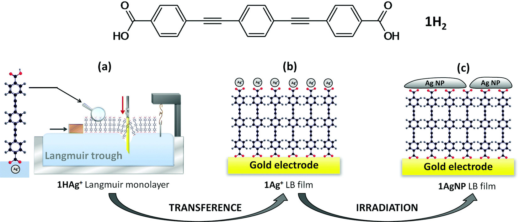 | ||
| Fig. 1 Top image: 4,4′-(1,4-Phenylenebis(ethyne-2,1-diyl))dibenzoic acid (1H2). Bottom image: Schematic of the Au|monolayer|Ag device fabrication strategy: (a) Langmuir film of 1H2 spread onto an aqueous sub-phase containing AgNO3; the carboxylic acid in contact with the aqueous sub-phase is deprotonated and a double ionic layer incorporating the majority cation is formed, 1HAg+ film. (b) Transference of the 1HAg+ Langmuir film by immersion of a gold substrate into the water sub-phase results in the formation of a Langmuir–Blodgett (LB) monolayer in which the carboxylic group not immersed in the aqueous sub-phase is chemisorbed onto the gold substrate and the carboxylate group immersed in the aqueous subphase incorporates silver cations to maintain the electroneutrality of the system, 1Ag+ film. (c) Irradiation of the 1Ag+ LB monolayer results in photoreduction of the silver cations and formation of silver nanoparticles. The film is denoted as 1AgNPs. | ||
Compound 1H2 is a symmetric OPE derivative, which has been shown to form homogeneous and highly ordered Langmuir–Blodgett (LB) films.12 On the one hand, the proton associated with the carboxylic acid (–COOH) of 1H2 within the aqueous sub-phase is readily exchanged for other cations introduced into the aqueous sub-phase. If the majority cation in the subphase is Ag+, then a Langmuir film denoted as 1HAg+ is formed. These silver cations are transferred onto LB films to maintain the electroneutrality of the system. Silver cations also incorporate some water molecules as part of their hydration sphere.13 On the other hand, the tendency of carboxylic groups to chemisorb onto metals such as gold or silver is also well-known,14,15 and when the gold substrate is introduced in the water subphase the carboxylate group is chemisorbed onto the metal surface, which involves deprotonation of the terminal carboxylic acid to form 1Ag+ LB films. Subsequent photoreduction of the coordinated silver cations in 1Ag+ LB films results in the formation of disk-like metallic silver nanoparticles, which cover a significant portion of the film surface, and this system is denoted here as 1AgNP. The photoreduction mechanism of silver cations16 as well as the subsequent nucleation and growth mechanism of the silver nanoparticles17,18 have been studied in detail before. Fig. 1 summarizes the method proposed in this work for the fabrication of metal/monolayer/metal devices.
Experimental
The compound 4,4′-[1,4-phenylenebis(ethyne-2,1-diyl)]-dibenzoic acid (1H2) was prepared as described elsewhere.11 A Nima Teflon trough with dimensions (720 × 100) mm2 housed in a constant temperature (20 ± 1 °C) clean room was used to prepare the films. The surface pressure (π) of the monolayers was measured by using a Wilhelmy paper plate pressure sensor. Ultrapure Millipore Milli-Q® water (resistivity 18.2 MΩ cm) was used as sub-phase. The spreading solutions with a concentration of 10−5 M 1H2 were prepared in chloroform (HPLC grade, 99.9% purchased from Sigma and used as received). To construct the Langmuir films, the solution was spread drop-by-drop using a Hamilton micro-syringe held very close to an aqueous surface, allowing the surface pressure to return to a value as close as possible to zero between each addition. The spreading solvent was allowed to completely evaporate over a period of at least 15 min before compression of the Langmuir film at a constant sweeping speed of 0.02 nm2 molecule−1 min−1. The ΔV–A measurements were carried out using a Kelvin probe provided by Nanofilm Technologie GmbH, Göttingen, Germany. The direct visualization of the monolayer formation at the air/water interface was studied using a commercial micro-Brewster angle microscopy (micro-BAM) from KSV-NIMA, having a lateral resolution better than 12 μm.The films were deposited on solid substrates of quartz, mica, glass or gold depending on the characterization technique to be subsequently used, at a constant surface pressure by the vertical dipping method (substrates initially outside of the water sub-phase) with a dipping speed of 0.6 cm min−1. Gold substrates were purchased from Arrandee®, Schroeer, Germany and were flame-annealed at approximately 800–1000 °C with a Bunsen burner immediately prior to use to prepare atomically flat Au(111) terraces.19 X-ray photoelectron spectroscopy (XPS) spectra were acquired on a Kratos AXIS ultra DLD spectrometer with a monochromatic Al Kα X-ray source (1486.6 eV) using a pass energy of 20 eV. To provide a precise energy calibration, the XPS binding energies were referenced to the C 1s peak at 284.6 eV. UV-visible spectra were acquired on a Varian Cary 50 spectrophotometer and recorded using a normal incident angle with respect to the film plane. AFM images were obtained in Tapping and Peak-Force modes using a Multimode 8 microscope equipped with a Nanoscope V control unit from Bruker operating in ambient air conditions at a scan rate of 0.5–1.2 Hz. To this end, RFESPA-75 (75–100 kHz, and 1.5–6 N m−1, nominal radius of 8 nm) and ScanAsyst-Air-HR (130–160 kHz, and 0.4–0.6 N m−1, nominal radius of 2 nm) tips, purchased from Bruker, were used. In order to minimize tip convolution effects affecting the AgNPs width, data obtained from AFM image profiling have been corrected according to Canet-Ferrer et al.20 Electrical properties of the molecular junctions were recorded with a conductive-AFM (Bruker ICON) under humidity control, ca. 40%, with a N2 flow using the Peak Force Tunnelling AFM (PF-TUNA™) mode, and employing a PF-TUNA™ cantilever from Bruker (coated with Pt/Ir 20 nm, ca. 25 nm radius, 0.4 N m−1 spring constant and 70 kHz resonance frequency).
Cyclic voltammetry (CV) experiments were performed using a potentiostat from EcoChemie and a standard three electrode cell, where the working electrode was a bare Au(111) electrode, a monolayer modified Au(111) electrode, or a monolayer/AgNP modified Au(111) electrode. These working electrodes were connected to the potentiostat by means of a cable ended in a metallic tweezer that held the electrode. The reference electrode was Ag/AgCl, KCl (3 M) and the counter electrode was a Pt sheet.
Results and discussion
Langmuir films were formed from 10−5 M solutions of 1H2 in CHCl3 on both pure water and 4 × 10⁻⁴ M AgNO3 aqueous sub-phases. The surface pressure vs. area per molecule (π–A) isotherms obtained for the film from a pure water sub-phase features a lift-off at ca. 0.80 nm2 molecule−1 whilst the monolayer prepared on an AgNO3 aqueous sub-phase, shows the lift-off at a slightly smaller area, ca. 0.65 nm2 molecule−1 (Fig. 2). Fig. 2 also includes the surface potential isotherms recorded upon the compression process in both sub-phases. The significantly lower values for the surface potential of Langmuir films on the AgNO3 aqueous sub-phase in comparison to the pure water sub-phase are indicative of a better charge compensation of the double ionic layer in the presence of the silver salt, which could indicate silver ion complexation by the carboxylate head group.21 The surface potential vs. area per molecule (ΔV–A) isotherms clearly evidence the collapse of the monolayers at areas per molecule of 0.29 nm2 (which corresponds to a surface pressure of 22 mN m−1 in the π–A isotherm) and 0.36 nm2 (which corresponds to a surface pressure of 17 mN m−1 in the π–A isotherm) in water and AgNO3 aqueous sub-phase, respectively (abrupt decrease in the surface potential isotherms).22 Brewster angle microscopy (BAM) images confirm the formation of a homogeneous Langmuir film from 1H2 on the AgNO3 aqueous sub-phase, 1HAg+ film, without the presence of three-dimensional structures at surface pressures below the collapse of the monolayer (Fig. 3).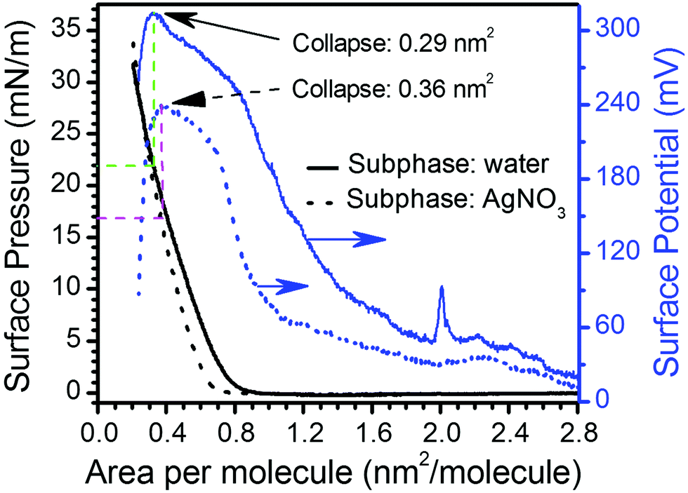 | ||
| Fig. 2 Representative surface pressure and surface potential vs. area per molecule isotherms formed from 1H2 on pure water (1H2) and 4 × 10⁻⁴ M AgNO3 (1HAg+) aqueous sub-phases. | ||
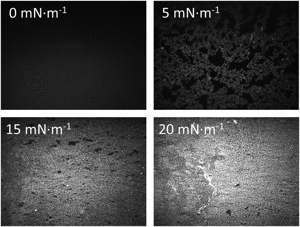 | ||
| Fig. 3 Brewster Angle Microscopy images of Langmuir films formed from 1H2 on an AgNO3 aqueous sub-phase (1HAg+) at the indicated surface pressures. The collapse of the monolayer can be observed in the bottom right image. The field of view along the x axes for the BAM images is 3300 μm. | ||
The Langmuir monolayers 1HAg+ were transferred onto solid substrates, that were initially held outside of the aqueous AgNO3 sub-phase, by the vertical dipping method at a surface pressure of 15 mN m−1 to form monolayer Langmuir–Blodgett films. The transfer ratio (defined as the decrease in monolayer area during the deposition divided by the area of the substrate) calculated using the trough software was 1. Under these transference conditions (substrates initially outside of the sub-phase) the carboxylic group not immersed in the aqueous sub-phase is directly attached to the substrate, denoted here as 1Ag+ films. XPS experiments confirm the chemisorption of a carboxylate moiety onto gold substrates, as reported previously.12
Fig. 4 shows the UV-vis spectrum of a pristine monolayer LB film of 1Ag+ transferred onto a quartz substrate from an AgNO3 aqueous solution as sub-phase. This spectrum features a band at 330 nm, which is likely to result from unresolved π–π* transitions associated with the OPE backbone,23 and observed at approximately the same wavelength as the analogous transitions of 1H2 in solution. Irradiation of the LB film 1Ag+ with UV light (254 nm) results in the appearance of a small broad peak at ca. 460 nm, attributable to surface plasmon resonance of silver nanoparticles.24 The plasmon peak reaches a maximum intensity after 15 minutes of irradiation.
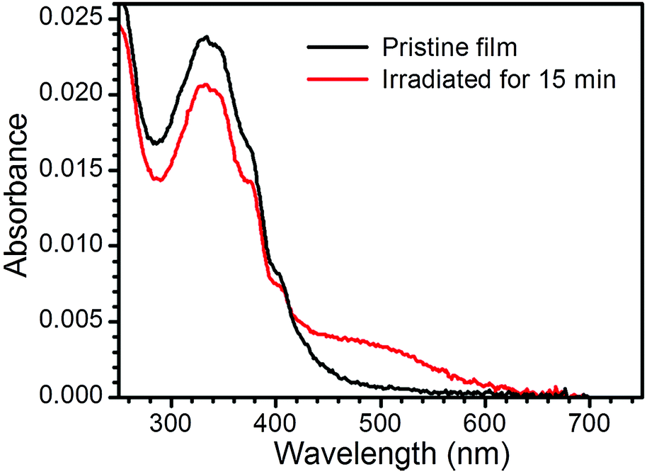 | ||
| Fig. 4 UV-vis spectra of a pristine single layer LB film of 1Ag+ and the same film after irradiation with UV light at 254 nm. | ||
The observation of a plasmon band is consistent with the formation of silver nanoparticles (AgNPs) on top of the LB film after irradiation. These films are denoted 1AgNP to distinguish them from the silver ion complexed films 1Ag+. Formation of metallic silver on these monolayers has also been demonstrated by XPS. Fig. 5 shows the XPS spectrum of irradiated LB films of 1AgNP on a gold substrate. The Ag(3d) region for the film after irradiation shows two peaks at 367.8 and 373.8 eV in good agreement with the peaks for Ag(0) reported in the literature.25,26 In addition, the area ratio of 4![[thin space (1/6-em)]](https://www.rsc.org/images/entities/char_2009.gif) :3 and the peak separation, 6 eV, is also consistent with metallic silver.25,26
:3 and the peak separation, 6 eV, is also consistent with metallic silver.25,26
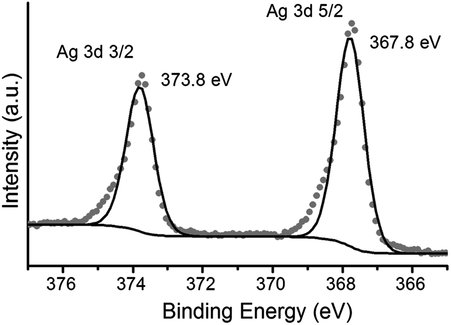 | ||
| Fig. 5 XPS spectrum of Ag(3d) photoelectrons of a one-layer LB film of 1AgNP, formed following transference of a LB film of 1Ag+ from an AgNO3 aqueous solution and irradiated at 254 nm for 15 minutes. | ||
However, neither UV-vis spectroscopy nor XPS provide any information about the distribution of the silver nanoparticles on the surface of the film of 1AgNP. To investigate this issue, the surface was studied by atomic force microscopy (AFM). Fig. 6a shows an AFM image of a LB film of 1Ag+ before and after irradiation. In comparison to the smooth and featureless surface exhibited by a pristine LB film of 1Ag+ (surface roughness, calculated in terms of the Root Mean Square (RMS), 0.4 ± 0.1 nm over areas of 300 × 300 nm2), after irradiation an organic-layer modified substrate homogeneously covered by disk-shaped particles closely assembled into a tightly packed 2D-arrangement, with low occurrence of irregular 3D Ag-aggregates is obtained. The RMS roughness of irradiated-film is 2.6 ± 0.2 nm, clearly much greater than that of the original 1Ag+ film. A statistical analysis of the AFM images reveal that these AgNPs have an average diameter of around 28 nm (corrected by the tip convolution) and an average height of ca. 6.9 nm (Fig. 6b and c). Additionally, AFM images indicate a large surface coverage by the silver nanoparticles. A bearing analysis of the AFM images was made. In a bearing analysis, the depths of all pixels of the image with respect to a reference point, i.e., the highest pixel are analysed. This kind of analysis renders an accurate estimation of the percentage of area covered by features, i.e. surface coverage, at every pixel depth.27,28 The bearing analysis of a one-layer LB film of 1AgNP gave an estimated surface coverage of 76% (see Fig. 7). This surface coverage value is significantly higher than that observed for the photoreduction of a gold precursor,11 which exhibited a surface coverage of 25%, indicating that silver has a larger tendency to form extended structures across the LB film. This result represents a step forward since this large surface packing of the silver nanoparticles may facilitate a subsequent step towards the complete metallization of monolayers by chemical vapour or electroless deposition processes without damaging the underlying organic monolayer.
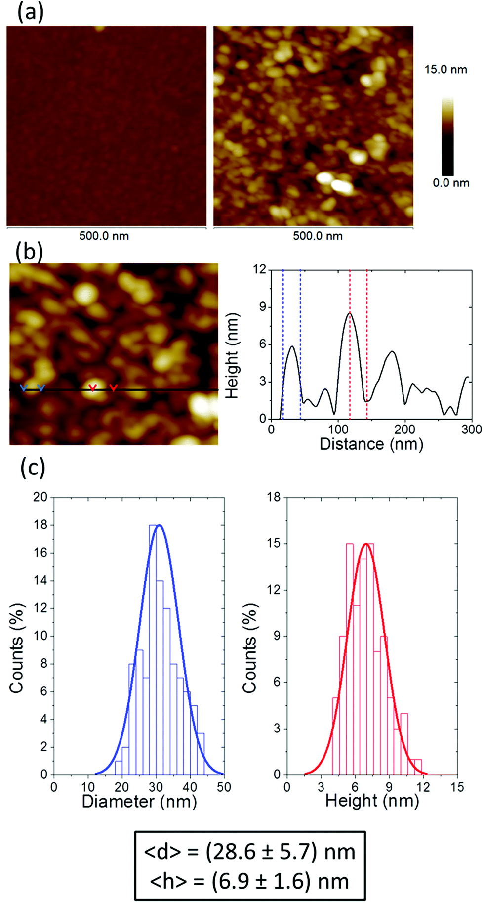 | ||
| Fig. 6 (a) 500 × 500 nm2 AFM images of a monolayer LB film of 1Ag+ transferred from an AgNO3 aqueous solution before (left panel) and after irradiation for 15 minutes at 254 nm (right panel). (b) Cross section of a representative AFM image and analysis profile illustrating the dimensions of the AgNPs. (c) Histograms showing the particle diameter (blue line) and height distribution (red line) corresponding to 100 AgNPs taken from different AFM images. Averaged NPs diameter and height values are depicted in the box below. | ||
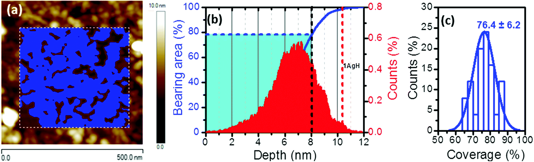 | ||
| Fig. 7 (a) 500 × 500 nm2 AFM images of a monolayer LB film of 1AgNP transferred from an AgNO3 aqueous solution and after irradiation for 15 minutes at 254 nm with the mask in blue unveiling nanoparticle-free molecule-modified areas. (b) Depth histogram showing the distribution of height data at different depth referred to a reference point, i.e. the highest pixel. The blue line (bearing analysis) indicates the relative projected area covered at each depth value depicted as a blue mask in the topographic image corresponding to the white-dashed boxed area. The small peak in the histogram marked with a red-dashed vertical line is attributed to the nanoparticle-free molecule-modified substrate while the black line accounts for the selected height threshold corresponding to half of the averaged height of the measured nanoparticles. (c) Histogram showing the average percentage of AgNPs-covered substrate area obtained for fifty equivalent but different 500 × 500 nm2 AFM images. | ||
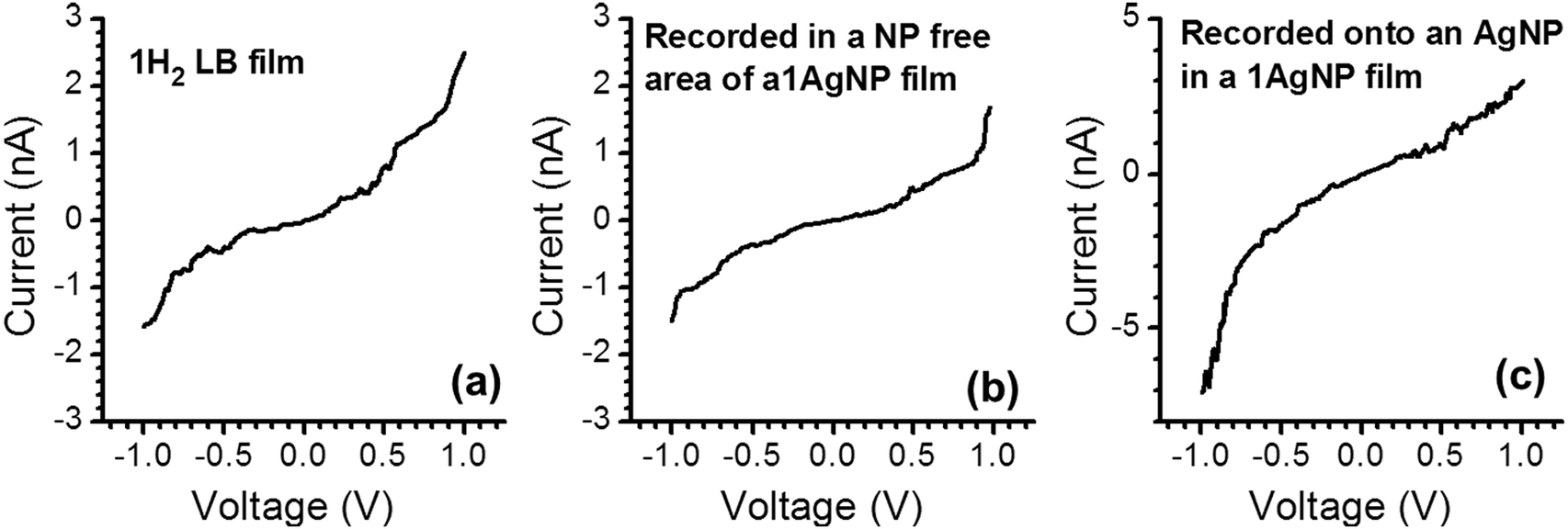
As noted above, a frequent difficulty encountered in the fabrication of metal–monolayer–metal devices is the deposition of the top contact electrode without the formation of short-circuits as a consequence of penetration of the growing top-contact electrode through the monolayer and subsequent contact with the underlying bottom electrode.29–31 Consequently, it is critical to verify whether the irradiation of an LB film of 1Ag+ to generate 1AgNP leads to short-circuits or if the layer-like arrangement of AgNPs formed from this soft photochemical method is an effective route towards a top-contact electrode. For that, I–V curves were recorded for these metal–monolayer–AgNPs structures using a conductive-AFM, c-AFM.32–36 The AFM system is equipped with a low noise current amplifier and Pt/Ir coated AFM tips were used, with a typical elastic contact value of around 0.5 N m−1 (PFTUNA, Bruker). Images were taken using the peak-force tapping mode, in which the tip makes intermittent contact with the surface at a frequency of 2 kHz. The maximum force (peak-force) is set typically below 10 nN, to limit damage to the surface and detrimental lateral forces. These characteristics make the peak-force tapping mode a useful strategy for the conductivity mapping of soft or fragile samples, since lateral forces are largely avoided. After acquiring an image, I–V curves were recorded by positioning the AFM tip on a specific location of the surface (for example, on top of an AgNP), establishing contact at a suitable force (usually larger than the peak-force value) and applying a bias between the LB-coated gold substrate and the tip. Too much force results in unacceptably large deformation of the monolayer underlying the AgNPs, while too little force yields an inadequate electrical contact between the AFM probe tip and the AgNP. Fig. 8 shows how an increase in the applied force results in a more effective contact between the tip and the AgNPs leading to a higher conductance. It is worth indicating here that these high forces (17.5 or 24 nN), required to make a reasonable contact, do not damage the organic layer during the determination of the electrical properties. Fig. 9c shows a representative I–V of all the curves (ca. 250 curves) recorded using a set-point force of 17.5 nN whilst Fig. 10 shows the conductance histogram built by adding all the experimental data in the −0.5 to 0.5 V ohmic region for each of the 250 I–V curves obtained experimentally at a set-point force of 17.5 nN. These I–V curves exhibit a linear section only at relatively low bias voltages and increasing curvature at higher bias, which is the common behaviour observed in metal–molecule–metal junctions. Importantly, no low resistance trace characteristics of metallic short circuits have been observed. In addition, Fig. 9a and b show a representative I–V curve registered for an LB film of 1H2 prepared onto a 0.1 M NaOH subphase and an I–V curve recorded on regions of the 1AgNP film not covered by AgNPs. These curves also exhibit the typical shape observed for metal–molecule–metal junctions, which rules out the presence of short-circuits and confirms that robust and reliable top-contacts have been prepared by photoreduction of a silver precursor without damaging the underlying organic monolayer film or altering/contaminating the interfaces.
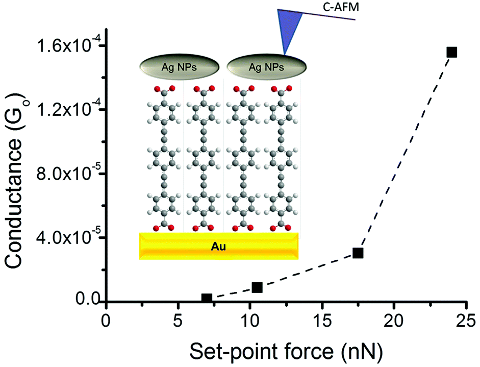 | ||
| Fig. 8 Average conductance values measured by locating the tip of the c-AFM on top of AgNPs at the indicated set-point forces. Inset: A scheme of the studied metal|1AgNPs structures. | ||
 | ||
| Fig. 9 Representative I–V curves for the indicated films. The set-point force used was 8 nN for (a) and (b) and 17.5 nN for (c). | ||
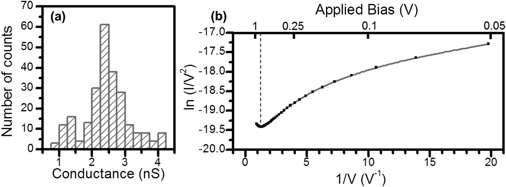 | ||
| Fig. 10 (a) Conductance histogram built from all the experimental data from −0.5 to 0.5 V for each I–V curve recorded (ca. 250 curves) positioning the tip onto an AgNP and applying a set point force of 17.5 nN. (b) The solid squares represent the average of 10 I–V curves for a 1AgNP device. The dashed vertical line corresponds to the voltage at which the tunnelling barrier transition occurs (Vtrans). | ||
In order to reinforce the conclusion that there are no metallic short circuits, a transition voltage spectroscopy (TVS) analysis has been made (Fig. 10b).37 It is known that the charge transport mechanism in electronic junctions of conjugated molecules undergoes a transition from direct tunnelling (rectangular barrier) to field emission (triangular barrier) upon increasing the applied bias. The voltage at which this transition occurs (Vtrans) is linearly correlated with the energy offset between the metal Fermi level and the highest occupied molecular orbital (HOMO).37 The obtained Vtrans from the TVS analysis, 0.84 ± 0.07 V, is in excellent agreement other similar OPE derivatives,38 which also rules out the presence of short circuits since short circuits would result in low values of Vtrans.
Cyclic voltammetry (CV) experiments have been used as a further confirmation that no significant alterations of the organic monolayer took place during the photoreduction process. Thus, CV experiments using working electrodes modified by the three different steps associated with the fabrication of the Au(111)/monolayer of 1AgNP devices were recorded in 0.1 M NaOH and the obtained results are presented in Fig. 11.
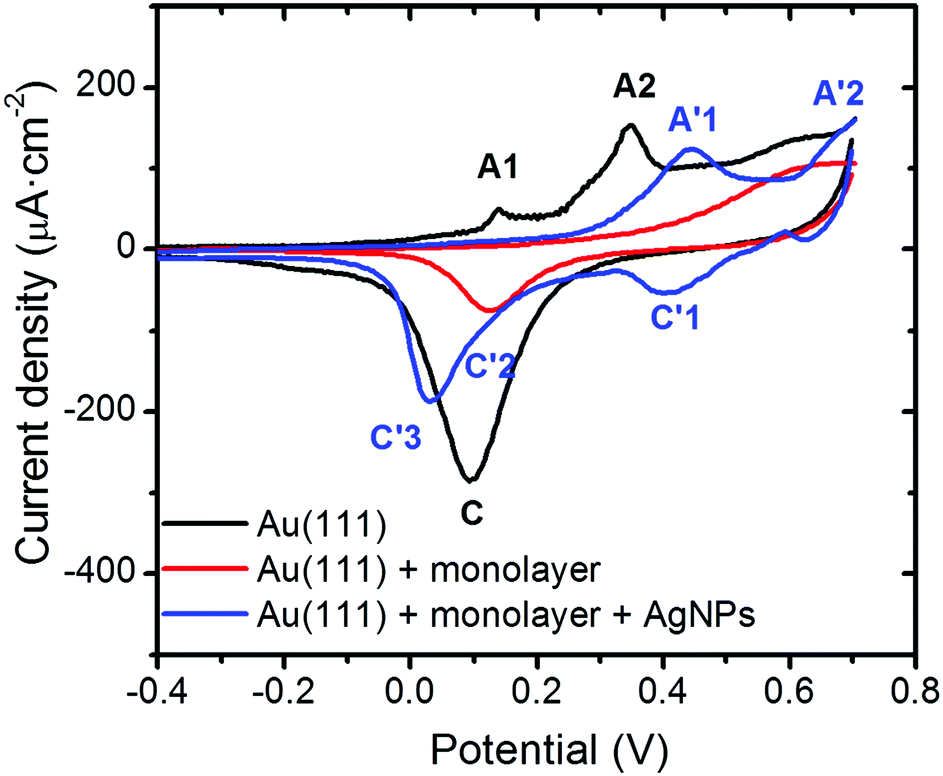 | ||
| Fig. 11 Black: cyclic voltammograms recorded for a bare Au(111) electrode. Red: monolayer of 1H2 transferred onto a Au(111) substrate. Blue: Au(111)/monolayer with overlying silver nanoparticles (1AgNP). All the voltammograms were recorded in a 0.1 M NaOH aqueous solution at 0.1 V s−1 using a Ag/AgCl, KCl (3 M) reference electrode. | ||
The electrochemical response recorded for the bare gold electrode corresponds well with that typically observed for Au(111)-oriented surfaces in alkaline media.39 In particular characteristic voltammetric peaks related to the gold oxide formation (nominally described here as AuO) are observed, identified with black letters as A1 and A2, as well as the corresponding electroreduction in the cathodic scan, labelled as C. Once the Au(111) electrode is modified with a single layer LB film, a dramatic decrease in the charge density along with a shift towards more positive potentials is observed for the electrochemical formation of the gold oxide monolayer. This corresponds to an inhibition of AuO formation since the surface is initially covered with a single layer LB film. At the most positive potentials (>0.5 V) current is seen to flow which could correspond to AuO formation and perhaps partial oxidation of the organic monolayer film. Since a peak is seen at the potential expected for AuO reduction in the reverse sweep it is reasonable to assume that the anodic peak at E > 0.5 V corresponds mainly to oxide formation on the gold surface beneath the organic monolayer. Finally, the electrochemical response of the AgNPs deposited onto the monolayer, resembles closely that previously reported for AgNP-based electrodes in alkaline media,40 since it exhibits two anodic and two cathodic voltammetric peaks marked (in blue) as A′1, A′2, and C′1, C′3, as well as a poorly resolved feature at C′2, respectively. Although the stoichiometry of the formed surface oxides are not well characterized for such conditions, based on the chemistry of silver these could correspond successively to the formation (A) and reduction (C) of the Ag(OH)2 and Ag2O monolayer, Ag2O multilayer, and finally the oxidation of Ag2O to AgO. Note that for this system the exposed silver surface area from the nanoparticles decorating the surface will be much larger than the smooth Au(111) substrate and as such the contributions from the formation of oxide on the underlying Au(111) surface are negligible compared to oxidation of the AgNPs in this voltammogram. Therefore, after the formation of AgNPs on the external surface of the single layer LB film (1AgNP), electron transfer through the organic layer occurs and, consequently, the applied electrochemical potential is experienced by the outer AgNPs/electrolyte interface as elegantly stated by Allongue et al.41 and supported by Gooding and co-workers.42 These results further confirm that the photoreduction of silver cations to metallic nanoparticles results in a robust sandwiched composite comprising a gold single-crystal, a tightly packed and almost defect free 2D-organic monolayer, and a silver-nanoparticle-based top contact.
Conclusions
In this contribution, photoreduction of a silver cation coordinated to a LB film terminated in a carboxylic group is shown to be suitable for the fabrication of a top-contact metal electrode in molecular junctions with a large surface coverage. Additionally, it has been shown that this method does not result in short-circuits which is a rather common problem in other traditional techniques for the preparation of top contact electrodes. The large surface coverage achieved would facilitate the subsequent application of other methods to achieve a complete metallization of the monolayer minimizing the risk of short circuits (e.g., electroless deposition, metal evaporation, etc.). Also the use of masks that allow the irradiation of the desired areas of the sample would result in the fabrication of arrays of devices.Acknowledgements
S. M. F. P.-M and P. C. are grateful for financial assistance from Ministerio de Economía y Competitividad from Spain and fondos FEDER in the framework of projects CTQ2012-33198, CTQ2013-50187-EXP, CSIC10-4E-805, and CSD2010-00024. S. M. and P. C. also acknowledge DGA and fondos FEDER for funding the research group Platón (E-54). R. J. N., P. J. L. and S. M.-G. thank EPSRC for funding (EPSRC Grants EP/K007785/1, EP/H035184/1, and EP/K007548/1). P. J. L. holds an ARC Future Fellowship (FT120100073) and gratefully acknowledges funding for this work from the ARC (DP140100855).References
- Editorial, Nat. Nanotechnol., 2013, 8, 385 CrossRef PubMed.
- D. Xiang, X. Wang, C. Jia, T. Lee and X. Guo, Chem. Rev., 2016, 4318 CrossRef CAS PubMed.
- H. Haick and D. Cahen, Prog. Surf. Sci., 2008, 83, 217 CrossRef CAS.
- D. Vuillaume, C. R. Phys., 2008, 9, 78 CrossRef CAS.
- H. B. Akkerman and B. de Boer, J. Phys.: Condens. Matter, 2008, 20, 013001 CrossRef.
- D. Vuillaume, Proc. IEEE, 2010, 98, 2111 CrossRef CAS.
- A. V. Walker, J. Vac. Sci. Technol., A, 2013, 31, 050816 Search PubMed.
- P. Cea, L. M. Ballesteros and S. Martin, Nanofabrication, 2014, 1, 96 CrossRef.
- L. M. Ballesteros, S. Martin, J. Cortés, S. Marqués-Gonzalez, F. Pérez-Murano, R. J. Nichols, P. J. Low and P. Cea, Adv. Mater. Interfaces, 2014, 1, 1400128 CrossRef.
- H. M. Osorio, P. Cea, L. M. Ballesteros, I. Gascon, S. Marqués-González, R. J. Nichols, F. Pérez-Murano, P. J. Low and S. Martín, J. Mater. Chem. C, 2014, 2, 7348 RSC.
- S. Martin, G. Pera, L. M. Ballesteros, A. J. Hope, S. Marqués-González, P. J. Low, F. Perez-Murano, R. J. Nichols and P. Cea, Chem. – Eur. J., 2014, 20, 3421 CrossRef CAS PubMed.
- L. M. Ballesteros, S. Martín, J. Cortés, S. Marqués-González, S. J. Higgins, R. J. Nichols, P. J. Low and P. Cea, Chem. – Eur. J., 2013, 19, 5352 CrossRef CAS PubMed.
- I. Person, Pure Appl. Chem., 2010, 82, 1901 Search PubMed.
- N. E. Schlotter, M. D. Porter, T. B. Bright and D. L. Allara, Chem. Phys. Lett., 1986, 132, 93 CrossRef CAS.
- S. A. Jadhav, Cent. Eur. J. Chem., 2011, 9, 369 CrossRef CAS.
- H. Hada, Y. Yonezawa, A. Yoshida and A. Kurakake, J. Phys. Chem., 1976, 80, 2728 CrossRef CAS.
- M. Harada and E. Katagiri, Langmuir, 2010, 26, 17896 CrossRef CAS PubMed.
- Y. Battie, N. Destouches, L. Bois, F. Chassagneux, A. Tishchenko, S. Parola and A. Boukenter, J. Phys. Chem. C, 2010, 114, 8679 CAS.
- W. Haiss, D. Lackey and J. K. Sass, J. Chem. Phys., 1991, 95, 2193 CrossRef CAS.
- J. Canet-Ferrer, E. Coronado, A. Forment-Aliaga and E. Pinilla-Cienfuegos, Nanotechnology, 2014, 25, 395703 CrossRef PubMed.
- P. Cea, S. Martín, A. Villares, D. Möbius and M. C. López, J. Phys. Chem. B, 2006, 110, 963 CrossRef CAS PubMed.
- G. Pera, A. Villares, M. C. Lopez, P. Cea, D. P. Lydon and P. J. Low, Chem. Mater., 2007, 19, 857 CrossRef CAS.
- A. Beeby, K. Findlay, P. J. Low and T. B. Marder, J. Am. Chem. Soc., 2002, 124, 8280 CrossRef CAS PubMed.
- S. Pal, Y. K. Tak and J. M. Song, Appl. Environ. Microbiol., 2007, 73, 172 CrossRef PubMed.
- B. de Boer, M. M. Frank, Y. J. Chabal, W. Jiang, E. L. Garfunkel and Z. Bao, Langmuir, 2004, 20, 1539 CrossRef CAS PubMed.
- R. G. Nuzzo and D. L. Allara, J. Am. Chem. Soc., 1983, 105, 4481 CrossRef CAS.
- S. Y. Heriot, H.-L. Zhang, S. D. Evans and T. H. Richardson, Colloids and Surfaces A: Physicochemical and Engineering Aspects, 2006, 278, 98 CrossRef CAS.
- M. Haro, B. Giner, C. Lafuente, M. C. Lopez, F. M. Royo and P. Cea, Langmuir, 2005, 21, 2796 CrossRef CAS PubMed.
- A. C. Dürr, F. Schreiber, M. Kelsch, H. D. Carstanjen and H. Dosch, Adv. Mater., 2002, 14, 961 CrossRef.
- A. V. Walker, T. B. Tighe, J. Stapleton, B. C. Haynie, S. Upilli, D. L. Allara and N. Winograd, Appl. Phys. Lett., 2004, 84, 4008 CrossRef CAS.
- C. Silien and M. Buck, J. Phys. Chem. C, 2008, 112, 3881 CAS.
- B. Pittenger, N. Erina and D. Su, Application Note Veeco Instruments Inc, 2010 Search PubMed.
- T. J. Young, M. A. Monglus, T. L. Burnett, W. R. Broughton, S. L. Ogin and P. A. Smith, Meas. Sci. Technol., 2011, 22, 125703 CrossRef.
- K. Sweers, K. van der Werf, M. Bennink and V. Bubramaniam, Nanoscale Res. Lett., 2011, 6, 270 CrossRef PubMed.
- G. Lee, H. Lee, K. Nam, J.-H. Han, J. Yang, S. W. Lee, D. S. Yoon, K. Eom and T. Kwon, Nanoscale Res. Lett., 2012, 7, 608 CrossRef PubMed.
- M. Lorenzoni, L. Evangelio, S. Verhaeghe, C. Nicolet, C. Navarro and F. Pérez-Murano, Langmuir, 2015, 42, 11630 CrossRef PubMed.
- J. M. Beebe, B. Kim, J. W. Gadzuk, C. D. Frisbie and J. G. Kushmerick, Phys. Rev. Lett., 2006, 97, 026801 CrossRef PubMed.
- J. M. Beebe, B. Kim, C. D. Frisbie and J. G. Kushmerick, ACS Nano, 2008, 2, 827 CrossRef CAS PubMed.
- P. Rodríguez, N. Garcia-Araez and M. T. M. Koper, Phys. Chem. Chem. Phys., 2010, 12, 9373 RSC.
- A. C. Joshi, G. B. Markad and S. K. Haram, Electrochim. Acta, 2015, 161, 108 CrossRef CAS.
- J.-N. Chazalviel and P. Allongue, J. Am. Chem. Soc., 2011, 133, 762 CrossRef CAS PubMed.
- A. Barfidokht, S. Ciampi, E. Luais, N. Darwish and J. J. Gooding, Anal. Chem., 2013, 85, 1073 CrossRef CAS PubMed.
| This journal is © The Royal Society of Chemistry 2016 |