
 Open Access Article
 This Open Access Article is licensed under a
 Creative Commons Attribution 3.0 Unported Licence
Synthesis of single crystalline In2O3 octahedra for the selective detection of NO2 and H2 at trace levels†
Sergio
Roso
ab,
Carla
Bittencourt
c,
Polona
Umek
d,
Oriol
González
a,
Frank
Güell
e,
Atsushi
Urakawa
 b and
Eduard
Llobet
*a
b and
Eduard
Llobet
*a
aMlnos-Emas, Universitat Rovira i Virgili, Av. Països Catalans 26, 43007 Tarragona, Spain. E-mail: eduard.llobet@urv.cat
bInstitute of Chemica Research of Catalonia (ICIQ), The Barcelona Institute of Science and Technology, Av. Països Catalans 16, 43007 Tarragona, Spain
cMateria Nova, Université de Mons, Parc Initialis, Avenue N. Copernic, 1, B-7000 Mons, Belgium
dDepartment of Solid-State Physics, Jožef Stefan Institute, Jamova cesta 39, 1000 Ljubljana, Slovenia
eDepartment D'Enginyeries, Electrònica, Universitat de Barcelona, C/Martí Franqès 1, 08028 Barcelona, Catalunya, Spain
First published on 9th September 2016
Abstract
Single crystalline indium oxide (In2O3) octahedra have been synthesized by means of a vapor phase transport method at high temperature. The resulting material has been characterized by FE-SEM, HR-TEM, XRD, XPS and PL. The gas sensing properties of this material against oxidizing and reducing gases have been examined and the conditions for selectively detecting such gases have been established. A high response towards NO2 has been obtained at a relatively low optimal operating temperature (i.e., 130 °C) and even at room temperature. The fact that the response of the nanomaterial is more than two orders of magnitude higher for NO2 than for H2, even in the presence of ambient moisture, makes it very promising for the selective detection of oxidizing species (at ppb levels) under real ambient conditions. The addition of noble metal nanoparticles (Pt and Pd) combined with an increase in the operating temperature (i.e., 250 °C) significantly increases H2 sensitivity and dramatically decreases the response to NO2. However, in this case, the presence of humidity negatively affects the response to H2. The sensing mechanisms are introduced and discussed.
Introduction
Semiconductor metal oxides have become fascinating materials due to their application in numerous fields such as gas sensing, heterogeneous catalysis and solar cells among many others. Considering their application in gas sensing the presence of oxygen vacancies on the oxide surface plays an important role in the sensing mechanism.1 In the case of n-type semiconductors, in the presence of oxidizing gases, for instance NO2, electrons are withdrawn from the conduction band, resulting in an increase in the resistivity of the metal oxide.2 In contrast, when the metal oxide is in contact with a reducing species, such as H2, the gas reacts with the oxygen adsorbed at the surface of the material, resulting in a decrease in its electrical resistivity.3,4Nanostructured materials have attracted attention over the past few years, in an attempt to overcome some of the drawbacks found when sensing gases employing bulk materials. Nanomaterials show higher surface activity, superior responsiveness at lower operating temperatures (i.e. require lower power consumption) and superior long-term stability than their bulk counterparts. Among all metal oxide semiconductors, indium oxide (In2O3) is one of the most important n-type, wide direct band-gap (around 3.6 eV at room temperature) semiconductors due to its excellent electronic and optical properties. The concern for environmental protection, human health and green energy has led to an increasing number of publications for an efficient gas detection of different toxic and volatile gases using In2O3 nanostructure based sensors. Many morphologies have been reported, including nanowires,5 nanofibers,6 nanotubes,7 nanoparticles, nanosheets, and nano-flower like structures8 among many others. However, little has been reported about the sensing properties of other polyhedral morphologies such as cubes, hexahedra, octahedra and dodecahedra.9 The advantage of using morphologies like octahedra is that they possess sharp edges and tips, which provides more active sites and smooth surfaces and unique and perfectly defined crystalline facets (i.e. (111)) exposed to the gas atmosphere.
Also, there is a lack of information regarding gas sensing properties under humidity conditions in previous In2O3 studies. A summary of the gas sensing properties of nanostructured In2O3 synthesized employing different methods is shown in Table 1. According to what has been reported on the detection of hydrogen and nitrogen dioxide with In2O3 films, there is no clear pattern on the optimum operating temperatures for the detection of these two gases.
| Synthesis method | Morphology | Target gas | Working temperature | Response | Ref. |
|---|---|---|---|---|---|
| a Response calculated as S = Ra/Rg − 1. b Response calculated as S = [(Ro − Rg)/Ro] × 100. c Response calculated as S = Rg/Ro. d Response calculated as S = Ro/Rg. e Response calculated as S = 1 − Ra/Rg. | |||||
| Laser ablation | Nanowires | NO2 (200 ppb) | Room temperature | −0.6a | 14 |
| Thermal evaporation | Nanotowers | H2 (2–1000 ppm) | 240 °C | 85%b | 15 |
| In situ oxidation | Nanoparticle | NO2 (100 ppm) | 300 °C | 32c | 16 |
| Sol–gel | Octahedra | NO2 (100 ppm) | Room temperature | 40c | 17 |
| AA-CVD | Thin film | NO2 (80 ppb) | 400 °C | 2c | 18 |
| Hydrothermal | Flower-like | NO2 (200 ppb) | 140 °C | 40c | 19 |
| Ammonolysis and re-oxidation | Octahedra strings | HCHO (100 ppm) | 420 °C | 1.8d | 20 |
| CVD | Nanoneedles | H2 (350 ppm) | 200 °C | 0.25e | 21 |
| Ionic layer deposition | Thin film | H2 (1000 ppm) | 450 °C | 8.5d | 22 |
| Hydrothermal | Nanocubes | H2 (5 ppm) | 150 °C | 25d | 23 |
| Vapor phase transport | Octahedra | NO2 (1 ppm)@50% R.H. | 130 °C | 120c | This work |
Even though pure metal oxide sensors can be very responsive to some gases, they often show poor selectivity. To overcome this drawback, noble metal particles can be added to the surface of the metal oxide active layer, improving their sensitivity towards a given target gas. Noble metals, such as Au,10 Pt10 or Pd,11 are usually added to metal oxide nanostructures through a variety of methods, among which RF sputtering is one of the most commonly used. Its effectiveness has been demonstrated when used for functionalizing metal oxide nanomaterials.12,13
Besides, In2O3 nanostructures show a strong photoluminescence (PL) emission in the visible range of the electromagnetic spectrum.24 This broad emission located mainly at around 580 nm is thought to be originated from different kinds of defects present in the material. Among them, oxygen vacancies, oxygen interstitials, indium interstitials and oxygen antisite may be responsible for the broad emission observed by PL25,26. These defects play a key role in the detection mechanism of semiconductor metal oxides. Therefore, PL studies can help to better understand the sensing mechanisms of indium oxide towards oxidizing and reducing agents.
In this work, we have synthesized In2O3 octahedra via vapor phase transport at high temperatures. The aim of the study is to shed light, for the first time, on the effect of the octahedral morphology on the gas sensing properties of In2O3 nanomaterials. Furthermore, it will be shown that the addition of Pt or Pd nanoparticles to the pure In2O3 octahedra can help tuning the gas sensing properties for the detection of hydrogen. PL measurements have been performed on sensors under operando conditions in the presence of air and NO2 diluted in air flows, in order to further confirm the sensing mechanism of In2O3 octahedra.
Experimental
In2O3 octahedra were synthesized on top of Si/SiO2 substrates via a vapor-phase transport method using a horizontal chemical vapor deposition (CVD) furnace. Si/SiO2 substrates were previously cleaned by sonication. The cleaning process follows three steps of 5 minutes each in acetone, ethanol and deionized water, and then dried in synthetic air. In a typical experimental procedure, 0.3 g of high purity In metal (99.99%) was placed on an alumina boat. Next to it, at a distance of around 1 cm the Si/SiO2 wafer was placed. Then, the alumina boat with the precursor and the wafer were placed at the center of the horizontal furnace. The temperature was raised to 1000 °C at a rate of 15 °C min−1, and kept constant for 120 min. The reaction took place in a dynamic Ar atmosphere (300 mL min−1).When the furnace was cooled down to room temperature, a pale green product was found on top of the Si/SiO2 wafer. The crystalline phase and morphological structural features were studied by means of X-ray diffraction (XRD, Bruker-AXS D8-Discover diffractometer with parallel incident beam), a field emission scanning electron microscope (FESEM, Jeol 7600F), and high resolution transmission electron microscopy (TEM and HR-TEM, JEOL 2100). For TEM and HR-TEM analyses, a methanol dispersion of the sample was ultrasonicated for 20 minutes and a drop of it was deposited on a lacy carbon film supported by a nickel grid. For SEM analysis a product was scratched from the Si/SiO2 substrate and placed on a carbon tape attached to an aluminum sample holder. Prior to the SEM investigation the sample was coated with a 3 nm thick carbon layer.
After that, the material was removed from the Si/SiO2 substrate and mixed in a solution of 1,2-propanediol. The resultant ink was used to deposit the material by screen printing on top of an alumina substrate with interdigitated Pt electrodes. At the back side of such a substrate, a Pt heater was placed in order to perform gas tests at different temperatures. It is worth saying that in each CVD synthesis, a quantity of 5–8 mg of In2O3 octahedra is obtained, and this is enough for producing 1–2 sensors.
After the screen printing deposition of the nanomaterial, a 6 μm thick layer is obtained on top of the alumina substrate. A SEM micrograph (cross-sectional view) can be found in the ESI.†
In order to deposit Pt or Pd nanoparticles on In2O3 sensors, an RF sputtering system was used. For Pt, 30 W and 8 s were used for the deposition and, for Pd, 50 W and 8 s were used, both under 3.75 mTorr and at room temperature. This process was conducted as a second step after the screen-printing of pure In2O3. The sputtering process parameters had been optimized previously for obtaining small and well-dispersed Pt or Pd nanoparticles, avoiding coalescence of the nanoparticles. It is not realistic to vary these parameters in view of altering Pd or Pt loading, as it is not the only variable that changes, particle size changes as well. It has been shown previously that sensing performance in Pd/SnO2 samples improves with decreasing Pd particle size.27 The amount of metal loading employed in the In2O3 sensors was guided by the results showing that reducing the amount of metal sputtered reduced the size of metal nanoparticles.
The chemical characterization of the active layers was performed using X-ray photoelectron spectroscopy (XPS); the XPS analysis was carried out using a Physical Electronics, VERSAPROBE PHI 5000 spectrometer equipped with monochromatic AlKα radiation with 0.7 eV energy resolution and a dual-beam charge-compensation system. All the XPS data were elaborated using Casa XPS v.2.3 software and binding energies were referenced with respect to the C 1s peak at 284.5 eV.
For obtaining the PL spectra, a Hd-Cd laser at 325 nm was used in order to overcome the band gap barrier of the In2O3 nanomaterial. The luminescence was dispersed using an Oriel Instruments 74![[thin space (1/6-em)]](https://www.rsc.org/images/entities/char_2009.gif) 000 monochromator and detected using a Hamamatsu H8259-02 with a socket assembly E717-500 photomultiplier. All sources of noise were removed using a Stanford Research System SR830 DSP lock-in amplifier.28 Sensors were hosted in a specially designed chamber fitted with a UV-quality quartz window, which allowed us to run PL measurements in the presence of either dry air or nitrogen dioxide diluted in air.
000 monochromator and detected using a Hamamatsu H8259-02 with a socket assembly E717-500 photomultiplier. All sources of noise were removed using a Stanford Research System SR830 DSP lock-in amplifier.28 Sensors were hosted in a specially designed chamber fitted with a UV-quality quartz window, which allowed us to run PL measurements in the presence of either dry air or nitrogen dioxide diluted in air.
Results and discussion
In2O3 nanostructures were synthesized via a vapor-solid mechanism, as indicated by the absence of the metal catalyst on the substrate. After melting of In grains, In vapor reacts with residual oxygen present in the furnace, thus forming oxidized clusters. When the temperature further increases, the oxidized In clusters act as nucleation centers for the formation of In2O3 crystals. The formation of In2O3 nuclei will lead to the formation of In2O3 with the desired morphology depending on the reaction temperature.29,30 At 700 °C, In2O3 triangular crystals are formed whereas at 800–1000 °C pyramids and octahedra can be obtained. The facets exposed correspond to the most energetically stable atomic planes in the lattice. Fig. 1 shows FESEM images of the In2O3 octahedra synthesized at 1000 °C. As shown, the final product consists of a high density of octahedral shaped structures (Fig. 1, upper panel). No other morphologies are observed, which indicates the uniformity of the process. A regular octahedron is composed of eight equilateral triangles, four of which meet at the same vertex. The side of each triangle is about 500 nm and all the faces are almost perfectly smooth and without any visible structural defects (Fig. 1, lower panel). Moreover, these structures possess sharp edges and vertexes.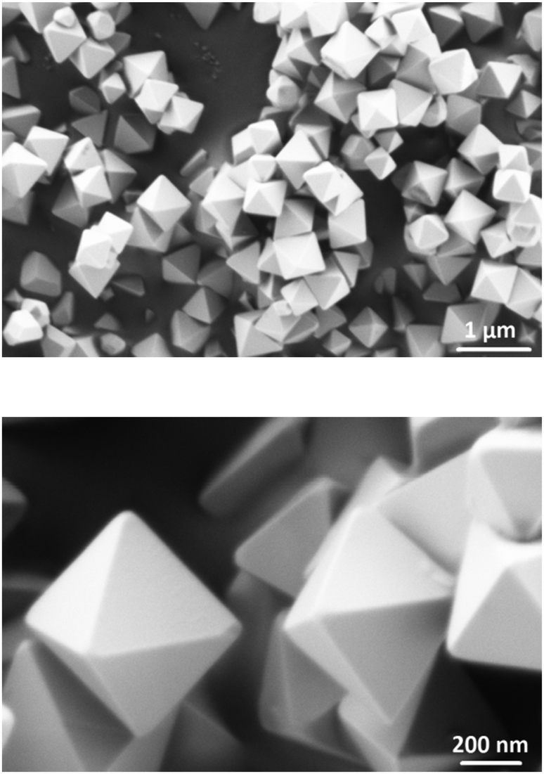 | ||
| Fig. 1 Low and high magnification ESEM images of the In2O3 octahedra. | ||
Further characterization has been carried out using TEM and HRTEM. Fig. 2 shows TEM and HRTEM images of the In2O3 octahedra. As observed, the side length of the octahedron is about 500 nm, which is consistent with that observed in the FESEM images. The inset of Fig. 2 exhibits a HRTEM image of the edge of the ocahedron. It clearly exhibits the continuous lattice fringes of the structures, showing the crystalline nature of the In2O3 octahedra. The distance measured between two adjacent fringes is 0.29 nm, which corresponds to the {111} interplanar distance of the cubic phase of In2O3 according to ICDD card no. 01-071-2194.
 | ||
| Fig. 2 TEM and HRTEM (inset) of the In2O3 octahedra. | ||
EDS carried out in an area of several In2O3 octahedra confirms that there are no impurities present as no other peaks other than those of indium and oxygen could be found (Fig. S2, ESI†).
Next, characterization of the sputtering-deposited Pt and Pd nanoparticles on top of the In2O3 octahedra was carried out. HR-TEM images of the Pt and Pd nanoparticles are shown in Fig. 3 and 4 respectively. As shown, after the deposition of Pt or Pd nanoparticles, the octahedral morphology was preserved. Furthermore, Pt nanoparticles appear to be homogenously distributed on the faces of the octahedra. The size of such nanoparticles is about 10–20 nm, as shown in Fig. 3. Closer inspection reveals that the measured interlayer distance is 0.26 thus corresponding to the {111} interplanar spacing of PtO according to ICDD card no. 43-1100.
 | ||
| Fig. 3 (a) FESEM image of the Pt/In2O3 octahedra, and (b) HR-TEM image of a Pt nanoparticle attached to an In2O3 octahedron. The inset shows the interlayer distance of the Pt nanoparticle. | ||
 | ||
| Fig. 4 (a) HR-TEM image of the Pd/In2O3 octahedra, and (b) HR-TEM image a single Pd nanoparticle attached to an In2O3 octahedron. | ||
By analyzing the Pd decorated samples we can observe that the Pd nanoparticles are also homogeneously distributed along the faces of the In2O3 octahedra. In contrast to the nanoparticles sputtered with a Pt target, these nanoparticles appear to be smaller, as their size ranges between 8 and 10 nm. Such nanoparticles have an interplanar spacing of 0.259 and 0.263 nm. Such lattice parameters are close to the interplanar spacing of tetragonal PdO (d111 = 0.263 nm and d002 = 0.266 nm according to ICDD card no 01-085-0624). In addition, according to Kibis et al.31 these values are characteristic of highly oxidized palladium nanoparticles where palladium is mainly in the +2 oxidation state.
The crystalline phase was confirmed by means of X-ray diffraction (XRD). As shown in Fig. 5, pure samples show the typical features of cubic In2O3. No peaks belonging to other materials or impurities could be found.
 | ||
| Fig. 5 XRD patterns of the pure In2O3 octahedra (top) and a commercial In2O3 powder (bottom). | ||
Additional XRD measurements for Pt and Pd-doped In2O3 samples were performed (Fig. S3, ESI†). These results confirm that metal decoration does not affect the crystallinity of In2O3 octahedra, which retain the cubic phase. Due to the low amount of metal loading, no peaks arising from Pt or Pd could be found. This is often the case for the typical amounts of metal loading used in gas sensing applications.20,32
With the aim to identify the chemical state of elements in the indium oxide and in the catalyst particles (Pt, Pd), XPS analysis was carried out on the nanostructures deposited on the sensor substrates. The In 3d core level spectra of both samples are shown in Fig. S5 of the ESI.† These are composed of two components, relative to the spin–orbit doublets (3d5/2 and 3d3/2), respectively, at 444.2 eV and 451.8 eV indicating that In is mainly found in the +3 oxidation state, which almost corresponds to the stoichiometric state.33 The O 1s XP spectra are comprised of two intense peaks centered at 529.8 eV and 531.8 eV (Fig. 6). The more intense peak has been ascribed to oxygen bonds in In–O–In, while the high binding energy peak at 531.2 eV is possibly partially related to oxygen vacancies in the bulk of metal oxides.34
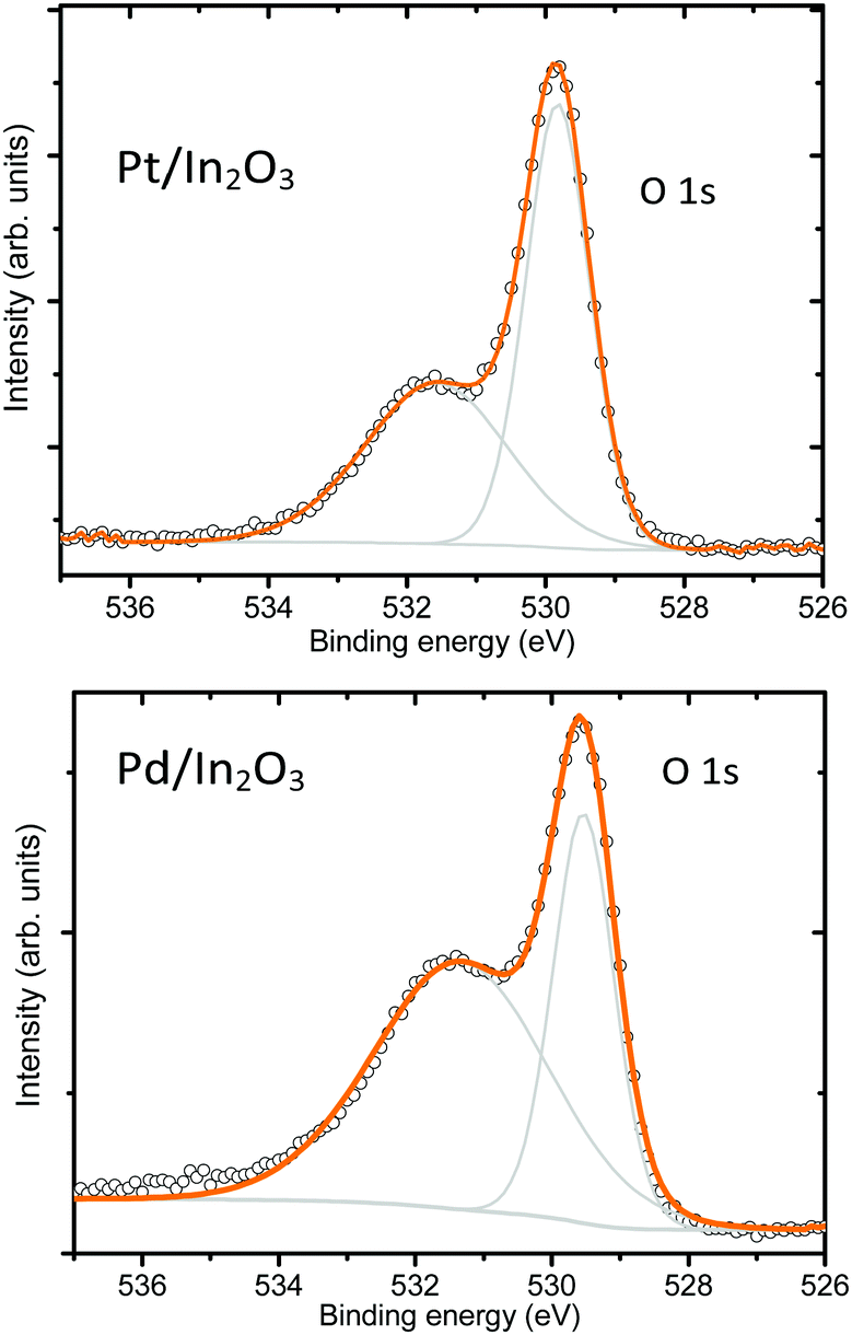 | ||
| Fig. 6 O 1s core level XP spectra of Pt/In2O3 and Pd/In2O3. | ||
By inspecting the Pt 4f XP spectrum we observe two doublets (Fig. 7), one with the 4f7/2 component at 71.2 eV and the other at 72.5 eV. The existence of these two doublets suggests the presence of a core–shell structure with the low-binding energy doublet assigned to photoelectrons emitted from Pt atoms in the core of the particles, while the high-energy component is assigned to an oxidized shell. Assignment to a particular platinum oxide is complex as several intermediate oxidation states between PtO and PtO2 have been reported to have peak positions in the range between PtO at 71.3 eV and PtO2 at 74.1 eV.35
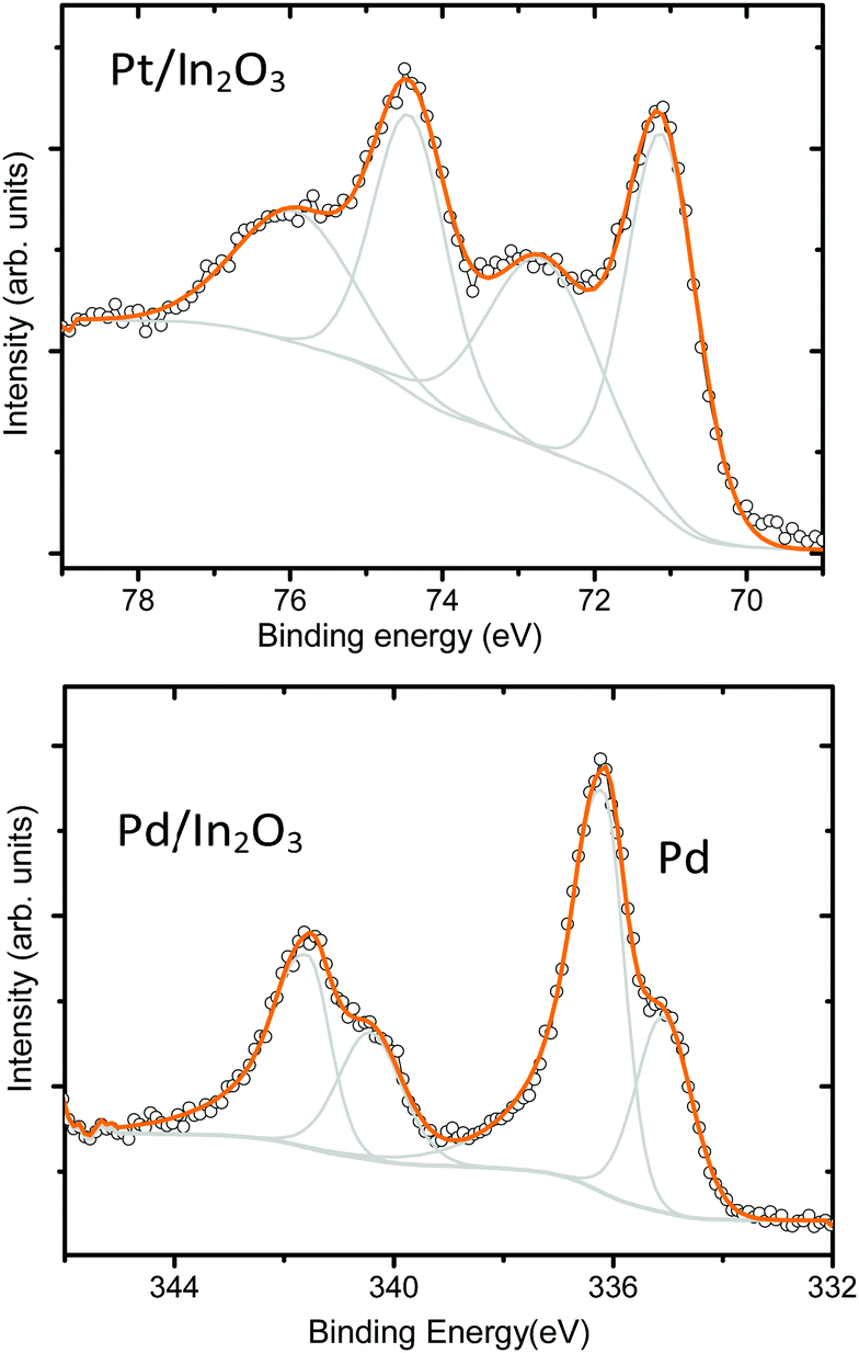 | ||
| Fig. 7 XP spectrum of Pt (4f) and Pd (3d). | ||
Conversely, in Fig. 7(b) the Pd 3d5/2 component at 336.2 eV clearly indicates the formation of PdO while the Pd 3d5/2 component at 335.1 eV indicates the presence of Pd0.36 Due to the small amount of Pt and Pd atoms deposited on the sample surface, the signal generated by photoelectrons emitted from oxygen atoms bound to Pt appears in the background of the O 1s peak. If we compare the XPS results recorded on the metal decorated samples with the ones recorded on the pristine In2O3 samples (shown in Fig. S4 in the ESI†), we observe that the decoration with metal nanoparticles has no influence in the oxidation state of the In2O3 octahedra.
Furthermore, in situ PL experiments under air conditions have been performed on sensors employing pristine In2O3, Pt or Pd decorated In2O3 octahedra. PL spectra were obtained for sensors operated at 130 °C in a flow of dry air.
Fig. 8 shows the normalized photoluminescence spectra of different indium oxide sensors operated at 130 °C in dry air. As one can observe, for the pristine In2O3 and the Pt decorated In2O3 octahedra, there is a strong PL emission at 600 nm whereas for the Pd decorated In2O3 octahedra, the strong emission occurs at 610 nm. This indicates that similar types of defects are present in the three samples. Such an orange emission band is thought to have its origin in deep In interstitials present in the nanomaterial.25
 | ||
| Fig. 8 PL spectra of the three sensors under dry air conditions. | ||
Finally, the In2O3 octahedra samples were subjected to gas sensing tests using oxidizing (NO2) and reducing (H2) gases by means of DC resistance measurements performed at different operating temperatures (100–250 °C). All sensors were exposed to 15 minutes of a given concentration of a species, followed by a 30 minute cleaning phase in dry air. All sensors showed an increase or decrease in resistance under exposure to oxidizing or reducing gases, respectively. This implies that In2O3 behaves as an n-type semiconductor.
The typical response and recovery cycles of an In2O3 octahedra sensor toward increasing concentrations of NO2 in dry air at 130 °C are presented in Fig. 9(a). It is well known that NO2 is a very oxidizing gas and can be easily adsorbed on In2O3 structures, which leads to a decrease of the electron density of In2O3 and thus, a decrease in conductance.
 | ||
| Fig. 9 (a) Response of the In2O3 octahedra sensor at 130 °C and (b) performance of the sensor as a function of temperature. | ||
The response and recovery time for all the concentrations is around 200 and 300 s, respectively, which is in the range of the response and recovery time of other studies of the In2O3 material.37,38 Furthermore, the baseline resistance can be recovered after exposing the sensor to dry air, which shows that the sensor is completely reversible. Also, it is seen that the signal to noise ratio is excellent. Fig. 9(b) shows the dependence of the In2O3 octahedra sensor as a function of different concentrations of NO2 as a function of different operating temperatures.
As shown in Fig. 9(b), sensors work optimum when operated at a relatively low temperature of 130 °C. Comparing these results with those available in the literature for similar In2O3 structures, Mu et al.17 reported a response that is 4 times lower with very slow response and recovery dynamics at room temperature for 100 ppb NO2. Bloor et al.18 reported a response that is 8 times lower at a much higher operating temperature (i.e. 400 °C). If we keep increasing the temperature, the performance sensors clearly worsen.
Moreover, gas sensing tests on low concentrations of NO2 at room temperature have been performed. As shown in Fig. S6 of the ESI,† the sensor achieves a response of Rgas/Rair = 2.46 when exposed to 200 ppb of NO2 in air. This shows that our nanomaterials have potential for detecting oxidizing species even when operated at room temperature.
It is important to note that our sensors are able to detect NO2 in the range of ppb with an excellent signal to noise ratio, which means that it is possible to detect even lower concentrations of this gas (the theoretical limit of detection can be estimated at units of ppb). A correlation between the logarithm of the sensor response and the concentration was easily obtained and it is shown in Fig. 10(a). As observed, a linear fit can be obtained from the response as a function of the concentration of NO2, with an r-square of nearly 0.99 in all the cases.
 | ||
| Fig. 10 (a) Response of the In2O3 octahedra sensor as a function of NO2 concentration and (b) performance of the sensor at 130 °C under humid conditions (50% R.H. at 22 °C). | ||
Furthermore gas sensing performance of an In2O3 octahedra sensor under humid conditions was examined by exposing it to NO2(g) in a background of air at 50% relative humidity (at 22 °C) and the response was compared to that under dry conditions. The sensitivity towards NO2 (the slope of the red curve in Fig. 10(b)) under humid conditions is significantly higher than that under dry conditions (the slope of the black curve in Fig. 10(b)).
Comparing the performance of the In2O3 octahedra sensors with that of sensors employing a commercially available In2O3 nanopowder (Sigma-Aldrich, 632317), it is observed that our nanomaterial shows a higher response under optimum working conditions, i.e. 130 °C, as shown in Fig. S7 of the ESI.†
Also, the performance of Pt and Pd-doped In2O3 octahedra sensors was examined under dry conditions. The responses obtained were extremely low compared to the response of pure In2O3 octahedra sensors under the optimum working conditions as presented in Table S2 of the ESI.†
Additionally, in situ PL experiments on the sensors under 100 ppm of NO2 target gas have been performed at 130 °C.
Fig. S8 of the ESI† shows the PL spectra of different indium oxide sensors operated at 130 °C in the presence of 100 ppm of NO2 in air. In this case, the strong PL emission is located at 600 nm for the three samples. This also suggests that the defects responsible for this emission are In interstitials.
As one can see, there is no significant difference between the normalized spectra under dry air shown in Fig. 8 and under NO2 concentration. This implies that there is no change in the concentration of In interstitials on the nanomaterial upon interaction with nitrogen dioxide. Also, the change in the number of oxygen vacancies caused by the presence of NO2 does not substantially modify the PL.
The sensing mechanism of semiconductor materials consists of two steps: the first one is the receptor function which involves the recognition of the species through gas–solid interaction, and the second one is the transduction function which involves the change in the electrical resistance of the sensor.13 At low operating temperatures (i.e., lower than 130 °C), when In2O3 octahedra are exposed to NO2(g), the gas becomes ionosorbed on the surface of the material due to its high electrophilic properties, resulting in an increase of the overall resistance of the sensor:
| NO2(gas) + e− → NO2(ads)− |
The rapid decrease in the response of the sensor at temperatures higher than 130 °C can be explained be the decreasing number of active sites for the adsorption of NO2 molecules. At higher temperatures, the amount of oxygen molecules adsorbed is greatly increased and as a consequence, the number of free active sites suitable for the adsorption of NO2 molecules is reduced. Therefore, the response of the sensor is sharply decreased. The presence of Pt or Pd nanoparticles on the surface of In2O3 favors, via a chemical sensitization, the increase in the number of adsorbed oxygen species at the surface of the metal oxide.13 This, once more, significantly reduces the number of active sites for the adsorption of NO2 and explains the dramatically reduced NO2 response observed for metal decorated samples.
Regarding the measurements under humid conditions shown in Fig. 9(b), at moderate operating temperatures (i.e. ≤200 °C), the interaction of ambient moisture with different metal oxide surfaces can be summarized as follows. The interaction with water vapor results in an increase of bridging hydroxyls and the formation of terminal hydroxyl groups.39,40 Also, dissociative adsorption of water takes place on surface metal atoms (Slat) giving rise to terminal OH groups. Assuming the dissociation of water molecules, hydroxyl surface groups are formed:
| H2Ogas + Slat + Olat ↔ (Slat+−OH−) + (OlatH)+ + e− |
In addition to the ionosorption of NO2 on the surface of the metal oxide, the following interaction mechanism might be possible between NO2 and the terminal hydroxyl groups:41
| NOgas2 + (Slat+−OH−) + (OlatH)+ + 2e− ↔ (Slat−NO2−) + H2Ogas + Olat− |
As a consequence, additional electrons are trapped via the conduction band of the metal oxide material, leading to an increase in NO2 response under humid air conditions.
Furthermore, the gas sensing properties of the In2O3 octahedra against a reducing gas such as H2 were investigated. The experiments were performed under the same conditions as those previously described for NO2. Fig. 11(a) shows the response of a sensor to low concentrations of H2 at 200 °C. The sensor resistance decreases with increasing H2 concentration, which is in agreement with the behavior of an n-type semiconductor exposed to a reducing gas. As in the case of NO2 sensing, the signal to noise ratio is excellent for H2 sensing, and the sensor will be able to detect concentrations in the ppb range (the theoretical limit of detection for hydrogen is in the tens of ppb range).
 | ||
| Fig. 11 (a) Response of the In2O3 octahedra sensor to different concentrations of H2 at 200 °C, and (b) response of the sensor as a function of the temperature. | ||
In contrast to NO2 sensing, the optimal operating temperature is higher for H2 sensing. The best performance of the sensor is found at the highest examined temperature of 250 °C (Fig. 11(b)). This suggests that we can make the sensor more selective to a target gas by properly choosing an operating temperature; low temperatures (e.g. 130 °C) will be optimal for NO2 detection, while higher temperatures (e.g. 250 °C) are suited for H2 detection. When operated at 130 °C and in a humid background, the sensor is very selective to selective oxidizing species because its response to 1 ppm NO2 is more than two orders of magnitude higher than its response to 1 ppm H2. When operated at 250 °C, the sensor becomes responsive to hydrogen. However, its response to nitrogen dioxide, although significantly decreases, remains of the same order of magnitude as that of hydrogen.
A possible approach to increase the sensitivity of In2O3 octahedra sensors to reducing gases like H2 is to load In2O3 with different noble metal nanoparticles. In this work, Pt and Pd nanoparticles have been chosen because they are well-known sensitizers for hydrogen detection in metal oxides.20,42
The lack of complete baseline recovery in both cases (worsens if the operating temperature is lowered) implies that the dynamics of sensor recovery is lower for H2 than for NO2 (Fig. 12).
 | ||
| Fig. 12 (a) Response of the Pt-doped In2O3 octahedra sensor to different concentrations of H2 at 200 °C, and (b) response of the Pd-doped In2O3 octahedra to different concentrations of H2 at 150 °C. | ||
Fig. 13 shows the comparison between pure In2O3 octahedra and Pt/Pd-doped In2O3 octahedra for H2 sensing. Both dopants improve the sensing characteristics of pure In2O3 octahedra. Particularly, it is easily observed that the best response in terms of H2 sensing is achieved with the Pt-doped In2O3 octahedra with the optimum temperature of 200 °C, lower than that of pure In2O3 octahedra. Recalling that metal loading resulted in a very significant decrease in sensitivity to nitrogen dioxide (see ESI†), Pt loading, in contrast, facilitates the selective detection of H2.
 | ||
| Fig. 13 Performance of the undoped and Pt/Pd-doped In2O3 octahedra sensors as a function of the operating temperature for H2. | ||
Moreover, the performance of Pt-doped In2O3 sensors operating in a humid background has been tested. The sensors operated at 200 °C were exposed to different concentrations of H2 gas (1, 2, 4, 10 and 20 ppm) in a background of air at 50% relative humidity (at 22 °C) as shown in Fig. 14. The sensor under 50% humidity shows significantly lower sensitivity (0.44 ppm−1) than the sensor under dry conditions (0.72 ppm−1).
 | ||
| Fig. 14 Comparison between the responses of the Pt-doped sensor under dry and humid conditions at 200 °C. | ||
Also, the response to H2 at 250 °C of Pt–In2O3 octahedra sensors is one order of magnitude higher than that of the same sensors to NO2 gas, as can be deduced from Table S1 in the ESI.† In other words, sensors become selective to reducing species (e.g. H2) by increasing the operating temperature and decorating the material with noble metal nanoparticles such as Pt.
It is generally accepted that reducing gases change surface conductivity due to a change in the oxidation state of the material. The fact that there is a sharp decrease in the response of the Pt-doped In2O3 sensor when exposed to H2 gas with 50% of relative humidity can be explained as follows: at relatively low temperatures, vapors of both H2 and H2O interact in the same way with the surface of the material, creating new OH groups and consuming the bridging oxygen atoms. As a consequence, the combined interaction of hydrogen and water vapors with the surface becomes competitive.39 Therefore, the response of the sensor is greatly decreased as shown in Fig. 14.
As previously stated, the sensing mechanism of n-type sensors is based on the variation of the electrical resistance of the sensing element, which depends basically on the gas atmosphere, the operating temperature and morphology of the sensing material among other factors. When the sensor is exposed to dry air, oxygen molecules adsorb on the surface of the material, capturing electrons of the conduction band. This creates a depletion layer derived from the adsorbed oxygen. As H2 is introduced in the measurement cell, H2 molecules react with the chemisorbed oxygen, releasing an electron back to the semiconductor, and thus, reducing the resistance of the sensor:39
| H2 + O− → H2O + e− |
However, we have experimentally seen that modifying the bare oxide with noble metal nanoparticles greatly enhances the response towards reducing gases. In this case, the gas–solid interaction that involves the receptor function is the catalytic oxidation of the target gas over the grain surface. When H2 molecules are in contact with the metal nanoparticles, they dissociate into H atoms that can spill-over to the semiconductor surface to react with the adsorbed oxygen. Therefore, the addition of the metal nanoparticle favors the reaction of the target gas with the semiconductor oxide via catalytic oxidation (chemical sensitization). In that way, the metal additive facilitates the interaction between the gas species and the semiconductor oxide. This type of interaction occurs mainly in the Pt-doped sensors.13
In a different mechanism, the metal additive in the oxidized state acts as a strong electron acceptor from the oxide creating a space charge layer. Then, the additive is reduced when it makes contact with the target gas; it relaxes the space charge layer by giving back the electrons to the semiconductor oxide. This type of interaction is named electronic sensitization and it occurs with noble metals like Pd. When Pd is exposed to dry air, it forms a stable metal oxide (PdO) that interacts with the In2O3 octahedra. When in contact with H2, they are converted back to the metallic state (Pd) resulting in the disappearance of the electronic interaction with In2O3.42 The results of the XPS analysis performed over the samples and shown in Fig. 7 confirm the presence of PtO and PdO on our sensors.
The reason why the response of the Pd-doped sensor is lower than the response of the Pt-doped one might be that the behaviour of the latter is a combination of the chemical sensitization and the electronic sensitization stated above.
In addition to the above-discussed chemical and electronic sensitization mechanisms, sensor response is also influenced by the amount of metal loading. However, the sputtering process was conducted in order to obtain nanoparticles with near to optimal sizes, according to previous studies.27,42
To further study the selectivity, all sensors were exposed to CO, EtOH, H2S, H2 and NO2, as shown in Fig. 15.
 | ||
| Fig. 15 Comparison between the responses of the Pt-doped, Pd-doped and pure In2O3 octahedra to several gases. Each colour represents a different gas. For each set of columns, the left one represents Pt-decorated In2O3 octahedra, the middle one represents Pd-decorated In2O3 octahedra and the right one represents pure In2O3 octahedra. | ||
In Fig. 15, one can see the response of the three types of materials exposed to several gases/vapors under their optimum working conditions. As observed, the best response is obtained for the pure In2O3 octahedra exposed to NO2 at a relatively low temperature (130 °C). Furthermore, a good response to ethanol vapors is also observed. However, the sensing temperature is much higher than that for NO2 and the concentration is two orders of magnitude higher.
If we focus only on the reducing species, we can see that at the same working temperature (200 °C), Pt-decorated sensors are able to detect 4 ppm of H2 with a good response, if we take into account that hydrogen concentration is nearly two orders of magnitude lower than that of EtOH, CO and H2S.
Conclusions
We have developed a facile method to synthesize high crystalline In2O3 octahedra at high temperatures, whose face size is around 500 nm. Furthermore, an easy way to decorate such nanostructures with noble metal nanoparticles has been shown. XPS measurements have shown that the metal nanoparticles have a core–shell structure in which the core of the particle corresponds to the metal and the shell corresponds to the oxidized metal.Additionally, we can say that pure In2O3 octahedra are excellent for detecting NO2 gas with outstanding sensitivity (0.43 ppb−1) at low temperatures (130 °C), while the response to H2 remains two orders of magnitude lower under the same conditions. In addition, the presence of humidity increases the sensitivity to NO2 and, at the same time, reduces the response to H2, which results in increased selectivity. This makes our sensor an excellent candidate to detect, in a selective way, oxidizing gases such as NO2 at low operating temperatures, even showing potential for room temperature operation, with excellent sensitivity even in the presence of humidity.
Furthermore, increasing the operating temperature and loading the octahedra with Pt, result in the quenching of the response to NO2 and in an increase in the response towards H2. In this way, one can make the sensor more selective to reducing gases such as H2. However, in this case the presence of ambient humidity negatively influences the response of the sensor.
As a consequence, our nanomaterial can be made selective to oxidizing or reducing gases by varying the operating temperature and by metal loading.
These significant differences revealed by this study suggest that engineering the morphology and the crystallinity of the material can be really useful and need further research, since it may become an effective strategy for enhancing the sensitivity and selectivity of In2O3 sensors.
Acknowledgements
This work has been funded in part by MINECO under grant no. TEC2015-71663-R. S. Roso and A. Urakawa would like to thank MINECO for support through Severo Ochoa Excellence Accreditation 2014-2018 (SEV-2013-0319). C. Bittencourt is a Research Associate of the National Funds for Scientific Research (FRS-FNRS, Belgium). S. Roso is also grateful for the URV-ICIQ fellowship. E. Llobet is supported by the Catalan Institute for Research and Advanced Studies via the ICREA Academia Award. S. Roso is also grateful to Dr Raúl Calavia for his help in conducting the experiments.References
- S. Pati, S. B. Majumder and P. Banerji, J. Alloys Compd., 2012, 541, 376–379 CrossRef CAS.
- D. Meng, N. M. Shaalan, T. Yamazaki and T. Kikuta, Sens. Actuators, B, 2012, 169, 113–120 CrossRef CAS.
- M. I. Baraton, L. Merhari, H. Ferkel and J. F. Castagnet, Mater. Sci. Eng., C, 2002, 19, 315–321 CrossRef.
- D. Caruntu, K. Yao, Z. Zhang, T. Austin, W. Zhou and C. J. O’Connor, J. Phys. Chem. C, 2010, 114, 4875–4886 CAS.
- X. C. Wu, J. M. Hong, Z. J. Han and Y. R. Tao, Chem. Phys. Lett., 2003, 373, 28–32 CrossRef CAS.
- C. H. Liang, G. W. Meng, Y. Lei, F. Phillipp and L. D. Zhang, Adv. Mater., 2001, 13, 1330–1333 CrossRef CAS.
- X.-P. Shen, H.-J. Liu, X. Fan, Y. Jiang, J.-M. Hong and Z. Xu, J. Cryst. Growth, 2005, 276, 471–477 CrossRef CAS.
- X. Xu, D. Wang, W. Wang, P. Sun, J. Ma, X. Liang, Y. Sun, Y. Ma and G. Lu, Sens. Actuators, B, 2012, 171–172, 1066–1072 CrossRef CAS.
- M. Shi, F. Xu, K. Yu, Z. Zhu and J. Fang, J. Phys. Chem. C, 2007, 111, 16267–16271 CAS.
- K. Yao, D. Caruntu, S. Wozny, R. Huang, Y. H. Ikuhara, B. Cao, C. J. O'Connor and W. Zhou, J. Mater. Chem., 2012, 22, 7308–7313 RSC.
- L. Liu, T. Zhang, S. Li, L. Wang and Y. Tian, Mater. Lett., 2009, 63, 1975–1977 CrossRef CAS.
- S. Vallejos, P. Umek, T. Stoycheva, F. Annanouch, E. Llobet, X. Correig, P. De Marco, C. Bittencourt and C. Blackman, Adv. Funct. Mater., 2013, 23, 1313–1322 CrossRef CAS.
- N. Yamazoe, G. Sakai and K. Shimanoe, Catal. Surv. Asia, 2003, 7, 63–75 CrossRef CAS.
- D. Zhang, Z. Liu, C. Li, T. Tang, X. Liu, S. Han, B. Lei and C. Zhou, Nano Lett., 2004, 4, 1919–1924 CrossRef CAS.
- Z. Q. Zheng, L. F. Zhu and B. Wang, Nanoscale Res. Lett., 2015, 10, 293 CrossRef PubMed.
- F. Li, J. Jian, R. Wu, J. Li and Y. Sun, J. Alloys Compd., 2015, 645, 178–183 CrossRef CAS.
- X. Mu, C. Chen, L. Han, B. Shao, Y. Wei, Q. Liu and P. Zhu, J. Alloys Compd., 2015, 637, 55–61 CrossRef CAS.
- L. G. Bloor, J. Manzi, R. Binions, I. P. Parkin, D. Pugh, A. Afonja, C. S. Blackman, S. Sathasivam and C. J. Carmalt, Chem. Mater., 2012, 24, 2864–2871 CrossRef CAS.
- X. Xu, X. Li, H. Zhang, C. Feng, C. Wang, F. Liu, Y. Sun, P. Sun and G. Lu, RSC Adv., 2015, 5, 30297–30302 RSC.
- W. Yang, P. Wan, X. Zhou, J. Hu, Y. Guan and L. Feng, Sens. Actuators, B, 2014, 201, 228–233 CrossRef CAS.
- A. Qurashi, E. M. El-Maghraby, T. Yamazaki and T. Kikuta, Sens. Actuators, B, 2010, 147, 48–54 CrossRef CAS.
- A. Shanmugasundaram, B. Ramireddy, P. Basak, S. V. Manorama and S. Srinath, J. Phys. Chem. C, 2014, 118, 6909–6921 CAS.
- G. Korotcenkov, V. Brinzari, S. H. Han and B. K. Cho, Mater. Chem. Phys., 2016, 175, 188–199 CrossRef CAS.
- S.-T. Jean and Y.-C. Her, Cryst. Growth Des., 2010, 10, 2104–2110 CAS.
- M. Kumar, V. N. Singh, F. Singh, K. V. Lakshmi, B. R. Mehta and J. P. Singh, Appl. Phys. Lett., 2008, 92, 171907 CrossRef.
- K. Yadav, B. R. Mehta and J. P. Singh, RSC Adv., 2015, 5, 1581–1586 RSC.
- N. Ma, K. Suematsu, M. Yuasa and K. Shimanoe, ACS Appl. Mater. Interfaces, 2015, 7, 15618–15625 CAS.
- S. Roso, F. Güell, P. R. Martínez-Alanis, A. Urakawa and E. Llobet, Sens. Actuators, B, 2016, 230, 109–114 CrossRef CAS.
- A. Qurashi, E. M. El-Maghraby, T. Yamazaki and T. Kikuta, J. Alloys Compd., 2009, 480, L9–L12 CrossRef CAS.
- A. Gurlo, Nanoscale, 2011, 3, 154–165 RSC.
- L. S. Kibis, A. I. Stadnichenko, S. V. Koscheev, V. I. Zaikovskii and A. I. Boronin, J. Phys. Chem. C, 2012, 116, 19342–19348 CAS.
- F. E. Annanouch, Z. Haddi, S. Vallejos, P. Umek, P. Guttmann, C. Bittencourt and E. Llobet, ACS Appl. Mater. Interfaces, 2015, 7, 6842–6851 CAS.
- D. V. Shinde, D. Y. Ahn, V. V. Jadhav, D. Y. Lee, N. K. Shrestha, J. K. Lee, H. Y. Lee, R. S. Mane and S.-H. Han, J. Mater. Chem. A, 2014, 2, 5490–5498 CAS.
- J. Gan, X. Lu, J. Wu, S. Xie, T. Zhai, M. Yu, Z. Zhang, Y. Mao, S. C. I. Wang, Y. Shen and Y. Tong, Sci. Rep., 2013, 3, 1021 Search PubMed.
- J. J. Blackstock, D. R. Stewart and Z. Li, Appl. Phys. A: Mater. Sci. Process., 2005, 80, 1343–1353 CrossRef CAS.
- G. B. Hoflund, H. A. E. Hagelin, J. F. Weaver and G. N. Salaita, Appl. Surf. Sci., 2003, 205, 102–112 CrossRef CAS.
- W. Zheng, X. Lu, W. Wang, Z. Li, H. Zhang, Z. Wang, X. Xu, S. Li and C. Wang, J. Colloid Interface Sci., 2009, 338, 366–370 CrossRef CAS PubMed.
- A. Gurlo, M. Ivanovskaya, N. Bârsan, M. Schweizer-Berberich, U. Weimar, W. Göpel and A. Diéguez, Sens. Actuators, B, 1997, 44, 327–333 CrossRef.
- R. G. Pavelko, H. Daly, C. Hardacre, A. A. Vasiliev and E. Llobet, Phys. Chem. Chem. Phys., 2010, 12, 2639–2647 RSC.
- P. A. Thiel and T. E. Madey, Surf. Sci. Rep., 1987, 7, 211–385 CrossRef CAS.
- A. Stănoiu, C. E. Simion and S. Somăcescu, Sens. Actuators, B, 2013, 186, 687–694 CrossRef.
- F. E. Annanouch, Z. Haddi, M. Ling, F. Di Maggio, S. Vallejos, T. Vilic, Y. Zhu, T. Shujah, P. Umek, C. Bittencourt, C. Blackman and E. Llobet, ACS Appl. Mater. Interfaces, 2016, 8, 10413–10421 CAS.
Footnote |
| † Electronic supplementary information (ESI) available. See DOI: 10.1039/c6tc03218d |
| This journal is © The Royal Society of Chemistry 2016 |