
 Open Access Article
 This Open Access Article is licensed under a
 Creative Commons Attribution 3.0 Unported Licence
Roll-to-roll infrared and hot-air sintering of gravure-printed Ag layer based on in situ tension measuring and analysis†
Janghoon
Park‡
a,
Hyi Jae
Kang‡
a,
Hyogeun
Gil
a,
Kee-Hyun
Shin
ab and
Hyunkyoo
Kang
*c
aDepartment of Mechanical Design and Production Engineering, Konkuk University, Seoul 143-701, Republic of Korea
bFlexible Display Roll-to-roll Research Center, Konkuk University, Seoul 143-701, Republic of Korea
cDigital Printing and Imaging Technology, Technische Universität Chemnitz, Reichenhainer Str. 70, 09126 Chemnitz, Germany. E-mail: hyunkyoo@gmail.com
First published on 19th September 2016
Abstract
This study presents a method developed to achieve the roll-to-roll sintering of printed Ag patterns based on exposure to hot air, near-infrared, and mid-infrared sources. The sintering energy was quantified and evaluated based on theoretical and experimental calculations. Moreover, the effect of the sintering energy on the web tension was simultaneously considered.
The sintering of a metal layer processed in a solution is necessary to improve its electrical performance in printed electronic devices.1 Several sintering (e.g. hot air,2 electric,3 microwave,4 and plasma5) and photonic [e.g. infrared (IR),6 ultraviolet (UV),7 laser8 and intense pulsed light (IPL)] techniques have been used.9–11 Recent research aimed at enhancing the effectiveness of the sintering performance achieved results within a few seconds6 or milliseconds,10 which means that the metal layers approached the conductivity of bulk metals.2
The roll-to-roll (R2R) system increasingly requires an effective sintering approach because of its limited processing footprint at the web span. In addition, a thermally damaged substrate affects the tension control performance by introducing strain and elastic modulus changes.12,13 Instability in the tension control can lead to a decline in the register control of the multi-layered printed layer,12 which eventually affects the yield of the electronic product.14 Considerable research has been devoted to the analysis of damage to the substrate according to the crack10 or peel strength15 of the layer responsible for the appearance of the final products.16 However, the web-handling performance (tension) in conjunction with the sintering performance has not been studied.
Our work involved the introduction of a large-area R2R inline sintering process, using a hot air oven [Fig. 1(a)] and photonic exposure [near-infrared (NIR) and mid-infrared (MIR), DTX Co. Ltd, Korea] [Fig. 1(b)]. An R2R gravure printing system (SungAn Machinery Co., Ltd, Korea)2 was used as the main platform. Gravure printing was conducted on a 300 mm width polyethylene terephthalate (PET) web (SH-34, SKC Co. Ltd, Korea) by using Ag paste (FLT-770G, FP Co. Ltd, Korea). The patterns printed on the PET substrate were dried and the substrate was rewound after the printing process. The length, width, and thickness of these printed patterns after gravure printing and drying at 90 °C for 2.5 min were 88 mm, 10 mm, and 1.67 ± 0.3 μm, respectively.
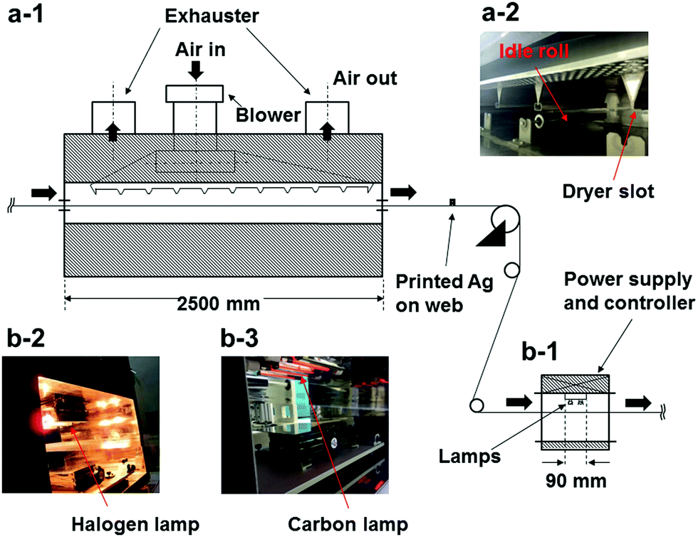 | ||
| Fig. 1 Schematic diagram and photographs describing a part of the large-area R2R sintering module on an Ag-layer printed on a moving plastic substrate, with (a-1) and (a-2) representing the hot air oven system with an effective exposure area of 350 × 2500 mm2, and (b-1) showing the photonic system with an effective exposure area of 350 × 90 mm2; (b-2) and (b-3) indicate the setup of the halogen and carbon lamps for the NIR and MIR sintering processes, respectively. | ||
The line resistances were measured six times within the sampled pattern on the lengthy film by using a source meter (2611A, Keithley Co. Ltd, USA). The resistance values decreased from the initial value of 2.8 ± 0.45 kΩ to 884 ± 118 Ω at a distance of 70 mm (between the lamp and the substrate) after 1.08 s of exposure time and 85 W of exposure power [Fig. 2(a)]. In all sintering cases, the highest conductivity with the shortest sintering time was obtained as 532 ± 21 Ω at 70 mm with 677 W power and 0.54 s sintering time. The standard deviation was very large (i.e. 21 Ω) for the resistance values of the overall patterns obtained after a short exposure time, because of the incompleteness of particle agglomeration. However, the deviation was minimised when the exposure time was increased. The resistance was 25 ± 2 Ω with 930 W power at a 35 mm distance when the exposure time was increased to 10.8 s. This result shows an improvement of approximately 2500%, compared to the samples sintered for 1.08 s. Linear scale plots of the line resistances plotted in Fig. 2 are provided in the ESI.†
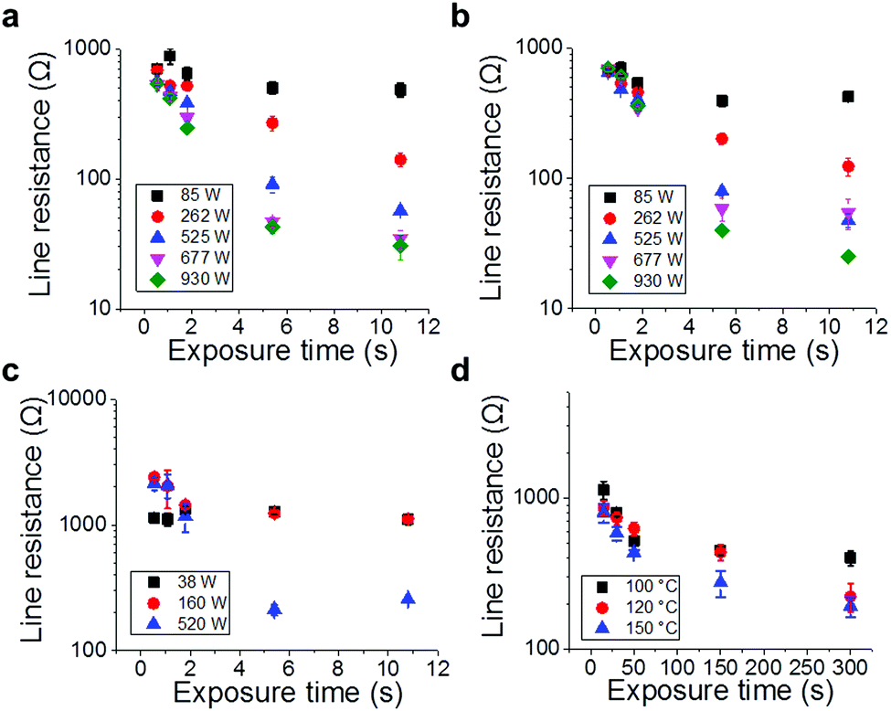 | ||
| Fig. 2 Semilogarithmic plot of line resistance as a function of the exposure time with different experimental conditions with respect to the power or temperature input. Photonic sintering with (a) NIR with a 70 mm distance between the lamp and the substrate, (b) NIR with a 35 mm distance and (c) MIR with a 35 mm distance using a different amount of power from the lamp. (d) Hot air in the oven chamber, showing the effect of the temperature changes. | ||
For the MIR sintering, the carbon lamp was set to 2.99 A at 174 V. For NIR sintering, the halogen lamp was set to 3.89 A at 174 V. The carbon lamp resistance was higher than that of the halogen lamp. Hence, the total power was different, even though the lamp voltages were the same. Moreover, the 70 mm distance with MIR exposure indicated less effectiveness. The line resistance at 520 W power did not decrease when the resistance was over 1 kΩ. Furthermore, no relationship was observed with respect to exposure times (see ESI†). A comparison of these two sintering methods showed a line resistance of 256 ± 11 Ω at a 35 mm distance, a 10.8 s exposure time, and 520 W power [Fig. 2(c)]. This value was poor compared to the NIR result obtained at a similar power, producing a result 540% worse than the 47.3 ± 11 Ω obtained with an NIR power of 525 W. The line resistance during hot-air sintering remained constant as the temperature and exposure times increased [Fig. 2(d)]. The best result obtained with hot air was 193 ± 29 Ω at 150 °C for 300 s.
The sintering performance could be quantified in terms of the energy density of the power source. An energy meter (Vega, OPHIR Photonics Co. Ltd, USA) was used to measure the photonic energy from the lamp across a 35 mm distance for a 1 s duration. The measured representative energy can be expressed as the curve fitting equation: e1 = (−3 × 10⁻⁶·P2 + 0.0072P + 1.5088)·3.52, where e1 is the measured power, and P is the input lamp power. Accordingly, the total energy density radiating from the lamp was calculated using eqn (1) as follows:6,17
 | (1) |
The temperature measured in the oven can be expressed as a curve-fitting equation to represent the rise from room temperature to 150 °C (Tc = 0.4883s + 18.806; Tc: temperature in °C, and s: time in seconds). As reported by Hebbar et al.,18 long ovens must achieve a thermodynamic equilibrium, in which the heat they emit must be equal to the total quantity of heat absorbed and lost by the web, oven wall, etc. The electrical heater of the oven supplied 60 kW, which formed the major input to the area. Thus, the heat loss from the wall and the web can be omitted to calculate the ambient temperature in the oven. In this manner, the required energy in the oven can be calculated by using the following equation:19
| E = cpρVΔT | (2) |
 | (3) |
 | ||
| Fig. 3 Energy exposure density as a function of the conductivity of the Ag pattern and the film deformation. (a) Line resistance for each experimental condition (i.e. NIR, MIR, and hot air oven). (b) Box charts of the line resistance and as various experimental sets (i.e. initial pattern, NIR, MIR and oven-sintered patterns). (c) Photograph of the tensile tester with a specimen of the Ag-printed and sintered sample. (d) Resulting box charts of the elastic modulus of the plastic web, wherein each of the Ag layers were printed and sintered. | ||
NIR radiation exposure was more effective in reducing the resistance than any other heat sources [Fig. 3(a)]. Interestingly, the NIR and MIR modules were more effective than the hot air oven, which supplied 60 kW power, even though they only provided about 1 kW electric power. The conductivity could not be calculated because of the roughness of the gravure-printed surface. Hence, the reduction in the relative line resistance was analysed in this study. Compared with the nano-sized ink particles, the flake particles required higher power and more time to agglomerate to larger-sized particles [see ESI†].2
The meta-equations of the NIR and MIR cases in the experiment can be suggested as follows as eqn (4) and (5), respectively, from the curve-fitted equation of Fig. 3(a):
| RNIR = 455.8e−0.054ED | (4) |
| RMIR = 1817e−0.041ED | (5) |
The box charts present information on the distribution of all the processed samples [Fig. 3(b)]. The average values showed that the exposure to NIR, MIR, and heat radiation in the oven resulted in an improvement of 516%, 150%, and 352% compared to the initial resistance (i.e. 2.8 kΩ). The results demonstrated that the MIR radiation can achieve a lower resistance. However, its standard deviation was high because of the incompatibility with the Ag layer and the PET film. As Cherrington et al. reported,20 the absorbance of infrared energy by the PET substrate increased as the wavelength increased from the NIR range to the MIR range. The same amount of MIR and NIR energy clearly affected not only the Ag layer, but also the PET substrate. An absorbance difference between the PET and the Ag layer was apparent (see ESI†). The PET absorbance in the 400–1100 nm wavelength range was almost negligible, in marked contrast to that of the Ag layer. Moreover, the NIR induced local damage near the Ag layer, whereas the MIR only caused shrinkage around the films.
The fully Ag-printed pattern was sintered and slotted with a size of 10 mm × 88 mm for the tensile test. The test was conducted according to ASTM D882 by using a universal tester [Instron 3343, USA, Fig. 3(c)].21 The standard deviation of the elastic modulus of the initial specimen was low (i.e. 81 MPa) compared with that of the sintered specimen (i.e. 136 MPa) [Fig. 3(d)]. The energy exposure modified the PET web properties in the form of expansion and shrinkage.2,13 The elastic modulus of the NIR-sintered specimen was obtained as 3.86 ± 0.135 GPa, which was the highest value for the experimental conditions. Meanwhile, the corresponding data for the samples subjected to MIR and heat exposure (oven) were 3.7 ± 0.136 and 3.76 ± 0.137 GPa, respectively.
The standard deviation of the elastic modulus of the sintered sample was similar overall, thereby implying the reliable significance of its value for each case. Exposure to NIR radiation clearly resulted in a higher elastic modulus because of the shrinkage attributed to the rapid temperature change with the effective energy absorbance by the Ag layer. The elastic modulus can affect the tension response of the R2R system. The linearized tension model in the upstream and downstream span [inset of Fig. 4(a)] can be expressed as follows:22
 | (6) |
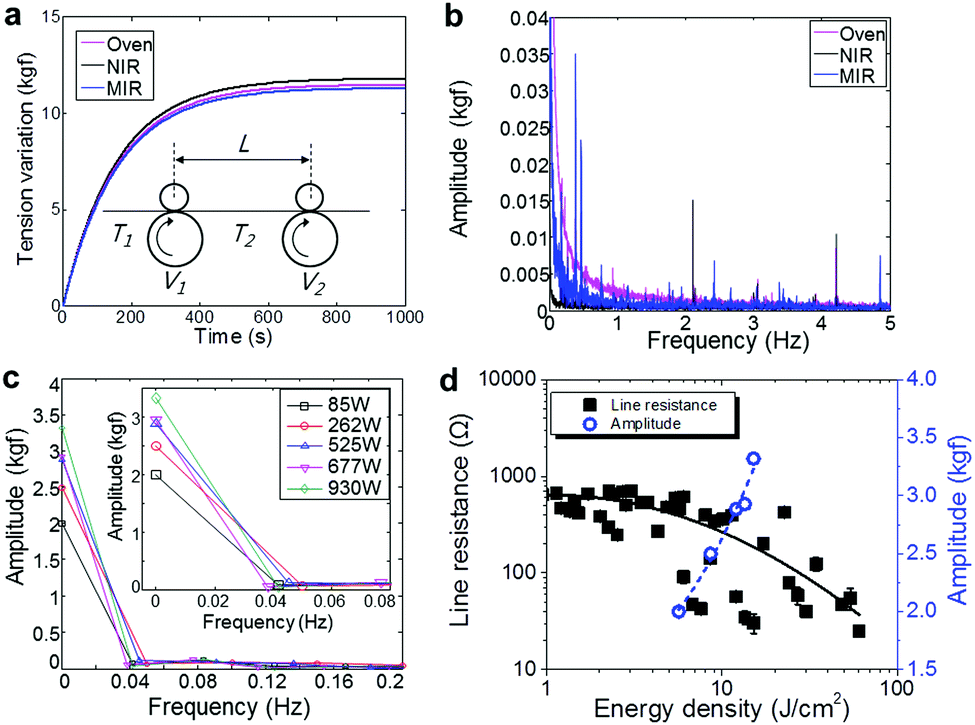 | ||
| Fig. 4 Effect of the sintering sources (i.e. oven, NIR and MIR) on the web property changes. (a) Step input response of T2 when V1 was changed by 1/1000 of the operating velocity [inset: schematic diagram of a free web span]. (b) FFT results for the PET substrate of the acquired tension data from the load cell with various sintering sources. (c) FFT results for the Ag-printed PET substrate of the acquired tension data with various NIR lamp powers (inset: zoomed graph from 0 Hz to 0.08 Hz). (d) Comparison between the line resistance of the Ag pattern and the amplitude as energy density. | ||
The simulation was conducted by considering the elastic moduli of the printed and sintered Ag patterns, wherein Ag was uniformly spread across the web substrate. However, the patterns were only partly located on the web according to the complexity of their pattern designs. A previous study6 found the PET substrate to be a good transmitter of NIR radiation, most of which was absorbed by the deposited Ag layer. The transmittance affected the tension variation of a moving substrate in the R2R system. The inline data acquisition for the R2R system, measured by using a load cell, showed the effect of the NIR radiation energy on the bare (not Ag printed) PET substrate [Fig. 4(b)]. A fast Fourier transform (FFT) was conducted using the web tension data for a 600 s driving time of the R2R system at a 5 m min−1 velocity. The measurement was started with the heat source turned on (full power: 930 W for the NIR and MIR and 150 °C for the oven). Among the conditions, the ‘oven’ data showed a high amplitude because of the long transient time taken to reach the specified temperature value. The tension markedly increased to 5 kgf after the oven was turned on for 300 s. This value was five times higher than the specified value. In addition, the MIR data indicated a higher peak than the NIR. The wavelength range of the MIR energy was suitable for PET absorbance. However, the bare PET film exhibited almost no damage after NIR radiation exposure. This result implied that the existence or non-existence of the printed pattern around the PET film can determine the extent of the damage caused by the photonic source, especially the NIR lamp. The effect of the patterned area on the amount of damage will be determined in further studies.
The line resistance of the Ag-printed patterns and the tension variation herein were simultaneously compared. The lamp power in Fig. 4(c) was varied to 85, 262, 525, 677, and 930 W. The tension data were acquired during the same time. The tension was measured with a 2 kgf operating tension, 2 m min−1 web velocity, and 35 mm distance. The FFT result clearly showed a relationship between the web tension and the lamp power. The energy density for each lamp power can be obtained as 5.7, 8.6, 12, 13.5, and 15.1 J cm−2 based on the experimental conditions. This result demonstrated that the line resistance and the tension variation were inversely proportional [Fig. 4(d)]. The tension value could be increased to 2, 2.5, 2.8, 2.9, and 3.3 kgf at a frequency of 0 Hz as the energy density increased, which indicated the mean tension value. These tension changes were clearly caused by a change in the elastic modulus of the PET when the PET web underwent expansion and shrinkage. The electrical performance of the electrode and the web handling performance should be considered simultaneously for the R2R sintering. Therefore, the production guidelines related to the conductivity of patterns or the operating tension ranges could determine the optimised energy density during the sintering process. As mentioned earlier, the areas of Ag and of the pattern will determine the NIR energy absorbance by the moving web. The exact absorbance rate could not be quantified at all times. Thus, these guidelines should be followed based on the exact experimental data and quality index (e.g. specific tension range), and the targeted electrical performance.
NIR, MIR, and hot air were compared as sintering sources for the Ag patterns on the moving PET substrate. NIR showed an excellent performance, which was obtained as 25 ± 2 Ω with 930 W power at a 35 mm distance. The quantification of each sintering method was also performed and compared. The results indicated that photonic sintering was the most effective technique for obtaining a good electrical performance, while NIR was the most efficient when the energy density was considered. Accordingly, the simulated and measured tension data obtained for the R2R system showed the advantages and disadvantages of NIR sintering with respect to the existence of an Ag pattern printed on the PET substrate. Sintering with a higher energy can improve the electrical performance of an electrode. However, the tension was varied with an amplitude of 0 to 1.3 around the set value of tension, according to the energy density change. Therefore, the perspective of tension variation and exact operating ranges should be considered when associating change with the web properties, as shown in this research.
Acknowledgements
This work was supported by the Alexander von Humboldt Foundation and the National Research Foundation of Korea (NRF) (2014K1A3A1A24068732). The authors also acknowledge the support of the Global Leading Technology Program funded by the Ministry of Trade, Industry and Energy, Republic of Korea (10042537) and the Leading Foreign Research Institute Recruitment Program through the National Research Foundation of Korea funded by the Ministry of Science, ICT & Future Planning (MSIP) (2010-00525).References
- S. Wünscher, R. Abbel, J. Perelaer and U. S. Schubert, J. Mater. Chem. C, 2014, 2, 10232–10261 RSC.
- J. Park, H. A. D. Nguyen, S. Park, J. Lee, B. Kim and D. Lee, Curr. Appl. Phys., 2015, 15, 367–376 CrossRef.
- S. Jang, D. J. Lee, D. Lee and J. H. Oh, Thin Solid Films, 2013, 546, 157–161 CrossRef CAS.
- S. Fujii, S. Kawamura, D. Mochizuki, M. Maitani, E. Suzuki and Y. Wada, AIP Adv., 2015, 5, 127226 CrossRef.
- S. Ma, V. Bromberg, L. Liu, F. D. Egitto, P. R. Chiarot and T. J. Singler, Appl. Surf. Sci., 2014, 293, 207–215 CrossRef CAS.
- E. Sowade, H. Kang, K. Y. Mitra, O. J. Weiß, J. Weber and R. R. Baumann, J. Mater. Chem. C, 2015, 3, 11815–11826 RSC.
- H.-J. Hwang, K.-H. Oh and H.-S. Kim, Sci. Rep., 2016, 6, 19696 CrossRef CAS PubMed.
- J. H. Choi, K. Ryu, K. Park and S.-J. Moon, Int. J. Heat Mass Transfer, 2015, 85, 904–909 CrossRef CAS.
- M. Hösel and F. C. Krebs, J. Mater. Chem., 2012, 22, 15683–15688 RSC.
- H. Kang, E. Sowade and R. R. Baumann, ACS Appl. Mater. Interfaces, 2014, 6, 1682–1687 CAS.
- D. Angmo, T. T. Larsen-Olsen, M. Jørgensen, R. R. Søndergaard and F. C. Krebs, Adv. Energy Mater., 2013, 3, 172–175 CrossRef CAS.
- J. Lee, J. Seong, J. Park, S. Park, D. Lee and K.-H. Shin, Mech. Syst. Signal Process., 2015, 60, 706–714 CrossRef.
- J. Lee, K. Shin and C. Lee, Rob. Comput.-Integr. Manuf., 2015, 35, 77–83 CrossRef.
- H. Kang, H. Park, Y. Park, M. Jung, B. C. Kim, G. Wallace and G. Cho, Sci. Rep., 2014, 4, 5387 CAS.
- J. Niittynen, R. Abbel, M. Mäntysalo, J. Perelaer, U. S. Schubert and D. Lupo, Thin Solid Films, 2014, 556, 452–459 CrossRef CAS.
- D. Bryant, I. Mabbett, P. Greenwood, T. Watson, M. Wijdekop and D. Worsley, Org. Electron., 2014, 15, 1126–1130 CrossRef CAS.
- H. Köstlin, R. Jost and W. Lems, Phys. Status Solidi A, 1975, 29, 87–93 CrossRef.
- H. U. Hebbar, K. Vishwanathan and M. Ramesh, J. Food Eng., 2004, 65, 557–563 CrossRef.
- L. Lin, J. Chen, Z. Xu, S. Yuan, M. Cao, H. Liu and X. Lu, J. Hazard. Mater., 2009, 168, 862–867 CrossRef CAS PubMed.
- M. Cherrington, T. C. Claypole, D. Deganello, I. Mabbett, T. Watson and D. Worsley, J. Mater. Chem., 2011, 21, 7562–7564 RSC.
- J. Lee, S. Park, J. Park, Y. S. Cho, K.-H. Shin and D. Lee, Int. J. Precis. Eng. Manuf., 2015, 16, 2013–2020 CrossRef.
- H.-K. Kang, C.-W. Lee, K.-H. Shin and S.-C. Kim, IEEE Trans. Ind. Appl., 2011, 47, 1558–1566 CrossRef.
- H. Kang and R. R. Baumann, Int. J. Precis. Eng. Manuf., 2014, 15, 2109–2116 CrossRef.
Footnotes |
| † Electronic supplementary information (ESI) available. See DOI: 10.1039/c6tc02464e |
| ‡ J. Park and H. J. Kang contributed equally to this work. |
| This journal is © The Royal Society of Chemistry 2016 |