
 Open Access Article
 This Open Access Article is licensed under a
 Creative Commons Attribution 3.0 Unported Licence
A high-performance self-powered broadband photodetector based on a CH3NH3PbI3 perovskite/ZnO nanorod array heterostructure†
Jichao
Yu‡
a,
Xu
Chen‡
a,
Yi
Wang‡
b,
Hai
Zhou
a,
Mengni
Xue
a,
Yang
Xu
a,
Zhaosong
Li
a,
Cong
Ye
a,
Jun
Zhang
a,
Peter A.
van Aken
b,
Peter D.
Lund
ac and
Hao
Wang
*a
aHubei Collaborative Innovation Center for Advanced Organic Chemical Materials, Faculty of Physics and Electronic Science, Hubei University, Wuhan 430062, China. E-mail: nanoguy@126.com
bStuttgart Center for Electron Microscopy, Max Planck Institute for Solid State Research, Heisenbergstr. 1, 70569 Stuttgart, Germany
cDepartment of Applied Physics, Aalto University, FI-00076 Aalto, Espoo, Finland
First published on 4th July 2016
Abstract
Here we report a self-powered photodetector based on a ZnO/CH3NH3PbI3 heterojunction and a MoO3 hole-transport layer. The organolead iodide perovskite photodetector is sensitive to broadband wavelengths from the ultraviolet light to the entire visible light region (250–800 nm), showing a high photo-responsivity of 24.3 A W−1 and a high detectivity value of 3.56 × 1014 cm Hz1/2 W−1 at 500 nm without external bias voltage. Meanwhile, we found that the photodetective performances are closely related to the thickness of the MoO3 layer, which acts as a hole-transport layer and an electron-blocking layer and can effectively decrease the recombination of holes and electrons. Additionally, the as-fabricated photodetector exhibits good stability and only 9.3% photoelectric response current decay after a 3-month illumination test. The high detectivity and responsivity of such a ZnO nanorod/perovskite heterojunction are clearly demonstrated and should be widely applicable to other photoelectric detection devices.
1. Introduction
Inorganic–organic perovskite materials, taking the structural form of CH3NH3PbX3 (X = Cl, Br, I), have attracted extensive attention for optoelectronic devices, such as light-emitting diodes, highly sensitive photodetectors and solar cells that have reached certified power conversion efficiencies above 20%.1–3 The low cost and facile solution-processing synthesis of these nanocrystals has opened up bright prospects for clean and sustainable energy production using CH3NH3PbX3.4 Meanwhile, the advantages of those perovskites, such as band gap engineering capabilities, large absorption coefficients, long carrier lifetimes, high carrier mobilities, and low recombination rates, make them promising candidates in optical and optoelectronic fields.5–7 Perovskite materials have excellent light absorbing characteristics and are strong sensitizers in the range from 300 to 800 nm, especially around 500 nm. It has been reported that the absorption rate of light could exceed 90%.8 The defect density in the energy band of perovskites is very low, resulting in low saturation current.9 A high-performance photodetector based on perovskite-graphene achieved a photoresponsivity of 180 A W−1, an effective quantum efficiency of around 5 × 10⁴%, and a photodetectivity of around 109 cm Hz1/2 W−1.5 An ITO/PEDOT:PSS/CH3NH3PbI3−xClx/PCBM/PFN/Al structure has been reported to reach even 4 × 1014 cm Hz1/2 W−1.10 However, the complexity of preparing organic materials and their instability have limited their practical applicability.Self-powered photodetectors have attracted increasing attention for their self-sufficient potential for operation, wireless performance, independency and sustainability.11,12 ZnO, a typical n-type transparent oxide semiconductor with a direct wide bandgap of 3.37 eV, is one of the most important nanomaterials and a promising candidate in self-powered p–n junction type ultraviolet photodetectors, benefiting from its unique characteristics, such as high resistance to irradiation, low deposition temperature, large exciton binding energy of 60 meV and a rich variety of nanostructure forms.11,13 An efficient p-type ZnO for photo-detection can be obtained by doping. Dr Shen developed a p-type ZnO/n-type ZnO homojunction structure with very good reliability.14
A hole-transport layer (HTL) plays a critical role in a p–n junction,15 as it enhances hole transport while blocks the backflow of electrons. PEDOT:DSS, spiro-OMETAD, and P3HT are commonly used HTL materials, while their strong acidity and hygroscopicity cause instability and they are harmful to the environment.16–18 The inorganic oxide MoO3 has attracted much attention as an HTL material in organic photovoltaic devices, which can effectively prevent the recombination of charge carriers at the electrode material interfaces for its specific energy band positions.19–21 Furthermore, MoO3 layers can protect the inner organic layers from air during the device fabrication processes.
In this paper, we have developed a photodetector based on a ZnO nanorod/perovskite heterojunction and a MoO3 film as the hole-transport layer to improve the photodetector device performance. The optimum thickness of MoO3 was 12 nm, resulting in a detector responsivity of 24.3 A W−1 and a detection sensitivity of 3.56 × 1014 cm Hz1/2 W−1. The detector can simultaneously detect UV and visible light, which could expand its applicability. In addition, the device had a relatively high response speed and it can be driven without an external bias voltage, thus saving energy.
2. Experimental
2.1 Growth of ZnO-nanorod arrays
Previous studies have reported hydrothermal methods for compounding ZnO-nanorod arrays.22–24 ZnO-nanorod arrays can also be synthesized by a simple water bath method. Firstly, an FTO glass was ultrasonically washed in deionised water, acetone, and ethanol for 20 min in sequence. Then, it was cleaned by UV-ozone for 15 min to remove organic matters attached to the surface of the FTO glass. 3 mM Zn(Ac)2 solution was prepared in advance using methanol as solvent. After stirring for 10 min, the solution was spin-coated on the FTO glasses at a rotational speed of 3000 rpm for 15 s and dried for 15 min at 100 °C. After that, they were annealed in a muffle furnace at 350 °C for 1 h to obtain ZnO seed layers on FTO glasses. The ZnO seed layer on FTO was used as a substrate for water bath growth of ZnO nanorod arrays. The precursor solution consisted of 50 mM Zn(NO3)2·6H2O, 30 mM of C6H12N4 and 0.6 g of polyetherimide (PEI). The pH of the solution was adjusted to 10.6–10.8 using ammonium hydroxide. Then the temperature of the solution was increased to 85–90 °C. Thereafter, the ZnO-nanorod arrays were obtained and washed with deionised water/ethanol. At last the ZnO-nanorod arrays were annealed in a muffle furnace at 350 °C for 2 h.2.2 Perovskite synthesis
The perovskite layer was prepared using the sequential deposition method.25 Firstly, methylamine (CH3NH2) (13.5 mL, 40 wt% in aqueous solution, Alfa Aesar) and hydroiodic acid (HI) (15.0 mL, 57 wt% in water, Alfa Aesar) were stirred at 0 °C for 2 h under a nitrogen atmosphere to synthesize methylammonium iodide (CH3NH3I) powder, as shown in eqn (1).| CH3NH2 + HI → CH3NH3I | (1) |
2.3 The depositions of the hole-transport layers and the Au electrode
MoO3 layers were deposited on the ZnO nanorod/perovskite heterojunction using the thermal evaporation method at a deposition rate of 0.2 Å s−1. Then a 40 nm thick Au layer electrode was deposited on top of MoO3 layers using the thermal evaporation method at a deposition rate of 0.8 Å s−1 under a pressure of 9.0 × 10⁻⁴ Pa. Finally, detector devices based on the ZnO-nanorod/perovskite heterojunction and MoO3 hole-transport layers were obtained.2.4 Characterization
The morphology of the samples was studied using a field emission scanning electron microscope (FESEM, JSM7100F Hitachi). The crystal structure of the thin film was measured using an A25 rotating anode X-ray powder diffractometer (XRD, Bruker D8). The I–V characteristics and the photoelectric response curves of the photodetector were measured using a Keithley 4200 electrometer. The light source was provided by a Xenon lamp power supply (No. 66984). And the tests were performed in air and at room temperature. Transmission electron microscopy (TEM) and high-resolution TEM (HRTEM) analysis were performed using a JEOL ARM 200F microscope equipped with a cold field emission electron source, an image Cs corrector (CEOS GmbH) operated at 200 kV. The TEM specimens of the ZnO/CH3NH3PbI3 sample were prepared by scratching the film, grinding into powder, and then dispersing the powder on a holey carbon copper grid under dry conditions.3. Results and discussion
The schematic diagram and working mechanism of the as-fabricated perovskite photodetector are illustrated in Fig. 1. A thin layer of ZnO seeds was firstly coated on the FTO glass by the spin coating method, followed by growing ZnO nanorods of about 1.5 μm in length and 80 nm in diameter. The one-dimensional ZnO nanorods were uniformly and perpendicularly grown on an FTO substrate, which could benefit the electrons harvest. CH3NH3PbX3 perovskite crystallized into the nanoparticle layer and filled the gap between ZnO nanorod arrays completely. The perovskite nanoparticles and ZnO nanorods formed a heterojunction structure. A thin layer of MoO3 was deposited on top of ZnO/perovskite composites to promote photon-generated carrier transport. Five different thicknesses of the MoO3 layer were carried out in our experiments, which were 5, 8, 12, 16 and 20 nm. An Au electrode was used as the top electrode. Perovskite absorbed light to generate electron–hole pairs under illumination. After that the excitons dissociated mainly at the ZnO/CH3NH3PbI3 interface and the remaining holes travelled across the perovskite layer before reaching the MoO3 hole-transporting layer. The specific energy band positions of the designed structure could benefit exciton dissociation and transport.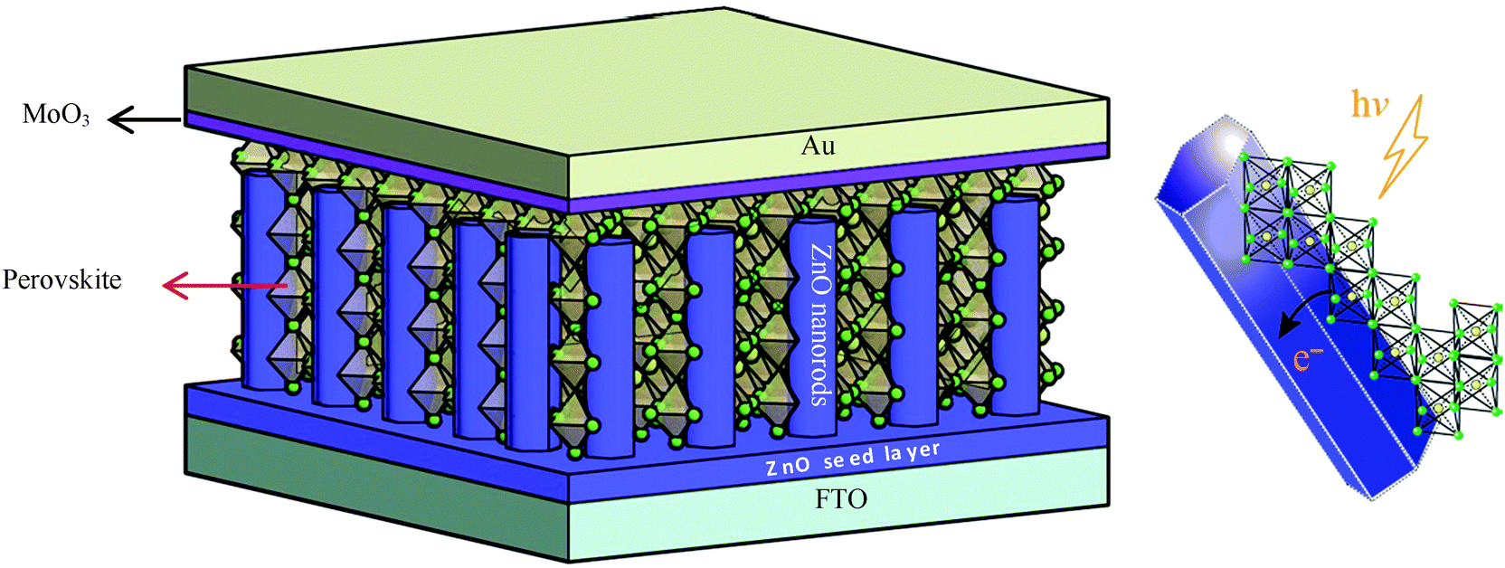 | ||
| Fig. 1 Schematic diagram and energy level diagram of the as-fabricated perovskite photodetector. | ||
Fig. 2 shows a SEM image of the pristine ZnO nanorods and after perovskite coating. As shown in Fig. 2(a), the top view of the ZnO-nanorod arrays demonstrates that the nanorods have a diameter of 80 nm and are uniformly deposited on the FTO glass. Fig. 2(b) shows a cross-sectional image of the ZnO nanorods, which have a length of 1.5 μm and are vertically grown on the substrate. The crystalline behaviour of the ZnO nanorods with hydrothermal/water-bath methods has been extensively studied and ZnO nanorods tend to grow along the ZnO[002] direction.26–28Fig. 2(c) shows the top view of the ZnO-nanorod array coated with perovskite, which crystallized into irregular polyhedron particles and covered the nanorod surface. The diameter of the polyhedron particles ranges from 80 to 250 nm. Fig. 2(d) shows the cross-sectional image of the ZnO/perovskite and it clearly shows that the CH3NH3PbI3 particle layer is fully immersed within the ZnO-nanorod arrays. As the perovskite particles completely immerse into the ZnO nanorod arrays, the transmission distance between electrons and holes is shortened, thus reducing their recombination and improving the detection performance of the device.
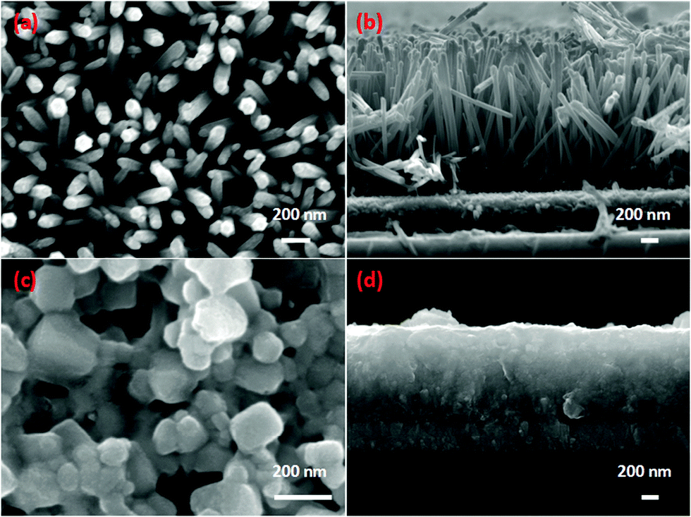 | ||
| Fig. 2 (a) Surface and (b) cross-sectional SEM images of the ZnO-nanorod array, and (c) surface and (d) cross-sectional SEM images of CH3NH3PbI3. | ||
XRD is used to characterize the structure of the ZnO nanorods and CH3NH3PbI3 perovskite, as shown in Fig. 3. The bottom XRD pattern confirms the pure ZnO nanorods grown on FTO substrates is a hexagonal structure and has a preferred (002) orientation (JCPDS No. 36-1451). A strong diffraction peak at 34.46° and another two weak peaks at 36.26° and 47.54° can be assigned to the (002), (101) and (102) planes of ZnO. The other three diffraction peaks appearing at 26.48°, 37.78° and 51.57° can be indexed to the FTO substrate (Fig. S1, ESI†). For the CH3NH3PbI3 perovskite coated with ZnO nanorods, we observe the appearance of a series of new diffraction peaks that are in good agreement with literature data and theoretically calculated values on the tetragonal phase of the CH3NH3PbI3 perovskite.24,29,30 The diffraction peaks appearing at 14.17°, 20.04°, 23.59°, 24.56°, 28.24°, 28.52°, 31.03°, 31.94°, 40.55°, 43.22° and 50.25° can be indexed to the (110), (112), (211), (202), (004), (220), (213), (222), (224), (314) and (404) planes of tetragonal CH3NH3PbI3, respectively. The diffraction peaks appearing at 12.70° and 39.58° belong to the residual PbI2. The absorption spectral curves of ZnO nanorods and ZnO-nanorod/perovskite heterojunction are shown in the ESI,† Fig. S2. ZnO nanorods exhibit a sharp absorption edge at 370 nm, which corresponds to the band gap of ZnO. For perovskite coated ZnO nanorods, the absorption edge demonstrates an obvious red shift.
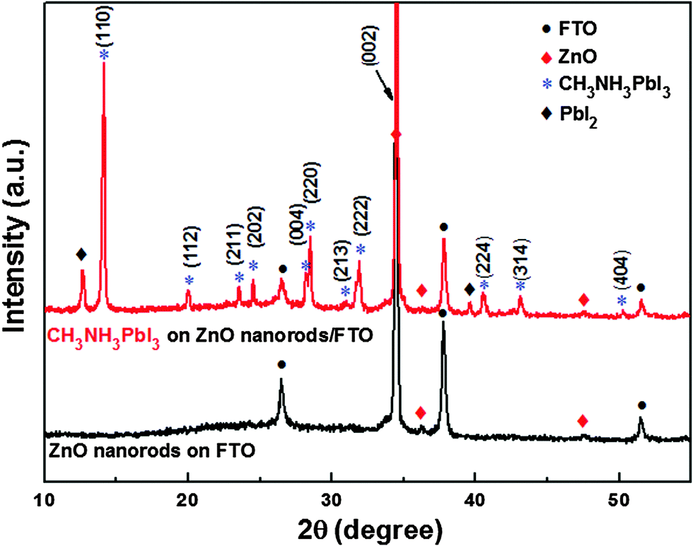 | ||
| Fig. 3 XRD pattern of the as-synthesized ZnO nanorod array and CH3NH3PbI3. | ||
The present results show that the ZnO nanorods and CH3NH3PbI3 perovskite were well crystallized. Further morphological and structural characterization of them was carried out by TEM analysis. A TEM micrograph of a ZnO-nanorod/CH3NH3PbI3 heterojunction at low magnification is shown in Fig. 4(a). Fig. 4(b) shows an HRTEM image of the ZnO nanorod highlighted in red in Fig. 4(a) and the lattice spacing is about 0.26 nm, which belongs to the d-spacing of the ZnO(002) plane. It proves that the ZnO nanorod grows along the c-axis direction and agrees well with the XRD characterization. From both low and high magnification images, one can see that some areas of ZnO give a slight different contrast, as highlighted by the yellow circles in Fig. 4(b) due to the covering of CH3NH3PbI3 nanoparticles on the surface of the ZnO nanorod. STEM-EDXS analysis further confirms the presence of CH3NH3PbI3 (see the STEM and EDXS analysis in the ESI†). Fig. 4(c)–(e) are HRTEM images of CH3NH3PbI3 nanoparticles from the selected area of Fig. 4(a) highlighted in green, blue, and pink, respectively. By measuring the lattice spacing and the angle between the different planes, possible lattice planes of the tetragonal phase of CH3NH3PbI3 have been indexed in the HRTEM images.
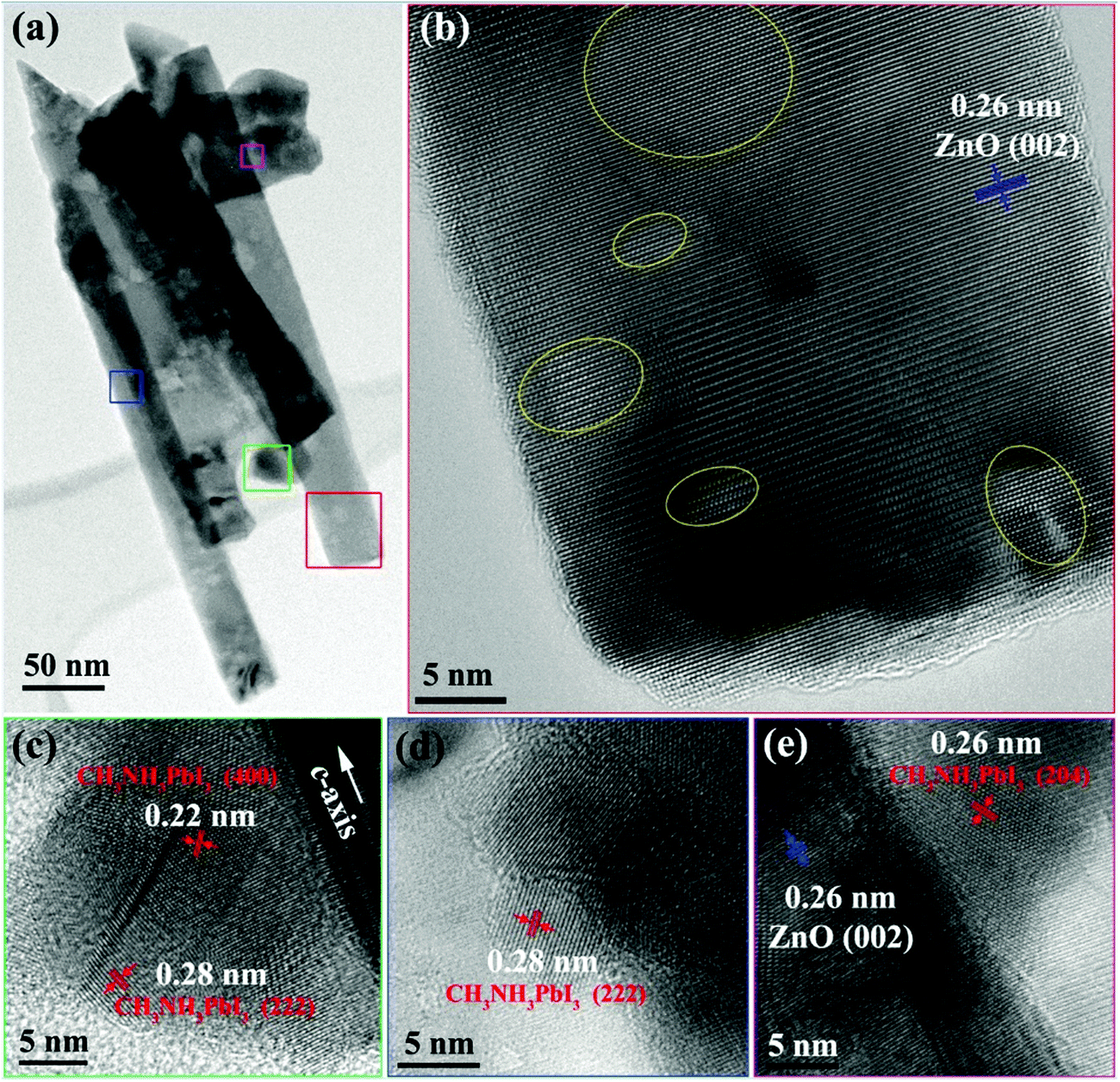 | ||
| Fig. 4 (a) TEM image of ZnO nanorods and CH3NH3PbI3 at low magnification, (b)–(e) HRTEM images of ZnO nanorods with CH3NH3PbI3 nanoparticles attached. | ||
Fig. 5 shows the I–V curves of as-fabricated detectors under dark conditions with the thickness of MoO3 ranging from 5 to 20 nm and the proposed working mechanism of MoO3. As shown in Fig. 5(a), J–V curves show favourable rectification characteristics, the rectification ratio reaching 500 at the bias voltage of ±1 V and the threshold voltages are around 0.5 V. With the thickness of MoO3 increasing from 5 nm to 12 nm, the reverse current gradually decreased and the forward current increased. With the thickness of MoO3 increasing from 12 nm to 20 nm, both the forward and reverse current decreased. In photoelectric detectors, the hole-transport layer plays a crucial role and the thickness of MoO3 has a significant influence on the performance of the detector.11,31–35Fig. 5(b) illustrates the working mechanism of the as-synthesized device with 12 nm MoO3. ZnO acts as the hole-blocking layer and MoO3 acts as the electron-blocking layer. Perovskite absorbs light to generate electron–hole pairs under illumination. Herein, the conduction band of MoO3 (∼1.66 eV) is much higher than that of perovskite (∼3.95 eV), also the valence band of MoO3 (∼5.4 eV) is close to the highest occupied molecular orbital of Au (4.5 eV). Thus, the presence of MoO3 benefits the hole transport and blocks the flow back of the electrons, which improve the performance of the detector. However, the thickness of the MoO3 film has a great influence on the performance of the device. For a thin MoO3 film, electrons can easily tunnel to Au (seen from Fig. 5(c)), resulting in the decrease of the photocurrent. Also if a thick MoO3 film is applied (seen from Fig. 5(d)), the transmission distance for holes and the equivalent serial resistance will increase, and many holes could not transport to the Au electrode due to the increase of carrier recombination. So the appropriate thickness is the best. In our experiment, the device with 12 nm MoO3 shows the best performance.
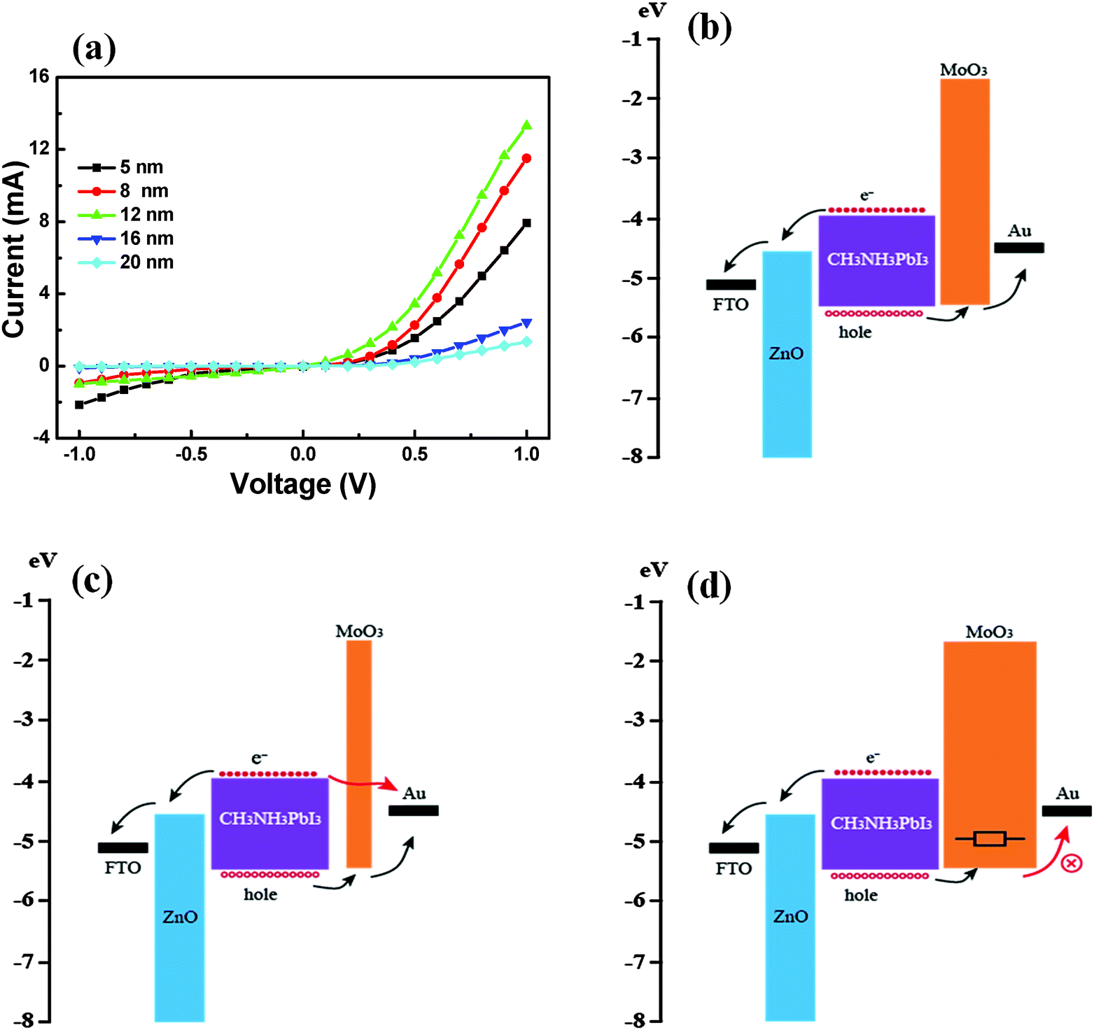 | ||
| Fig. 5 (a) I–V characteristic curves of as-fabricated detectors with the thicknesses of MoO3 ranging from 5 to 20 nm under dark conditions. The working mechanism of the detector when the thickness of MoO3 was 12 nm (b), less than 12 nm (c), and more than 12 nm (d). | ||
Responsivity (R) and detectivity (D*) are two key factors used when measuring the performance of a detector and can be calculated as given in eqn (2) and (3).6,36
 | (2) |
 | (3) |
Fig. 6 shows the responsivity (a) and detectivity (b) curves of the as-fabricated photodetectors with different thicknesses of MoO3 under zero bias voltage. From Fig. 6(a), we can see that the devices demonstrate a dual-function response to both UV and visible light and there are mainly two waves. The highest responsivity at 500 nm is 24.3 A W−1 with the 12 nm MoO3 layer. And the responsivity at 300 nm wavelength is 3.9 A W−1 high with 5 nm MoO3. The response in the UV region is mainly attributed to ZnO, while in the visible region the response is mainly attributed to perovskite. The detectivity can be given by eqn (3). The detectivity curve demonstrates mainly two peaks. One located at 300 nm is attributed to ZnO. The other around 500 nm is caused by the perovskite. We can see that from 800 to 500 nm, the value of the detectivity curve shows a continued increasing trend and reaches the highest at 500 nm. Perovskite materials show a strong light-capturing ability over the spectral region of 300–800 nm, in particular, they can absorb more than 90% of incident light at around 500 nm.37 The highest detectivity of 3.56 × 1014 cm Hz1/2 W−1 was obtained at 500 nm wavelength and the thickness of the MoO3 layer was 12 nm, meanwhile the photo-responsivity was as high as 24.3 A W−1. With the thickness of the MoO3 layer increasing from 5 nm to 12 nm, the detectivity increases, but starts to decrease with thicker MoO3 layers. It is ten-fold compared to a Si-based detector with a D* value of around 1013 cm Hz1/2 W−1. The 3.56 × 1014 cm Hz1/2 detectivity of our perovskite photodetector is among the highest values ever reported.6
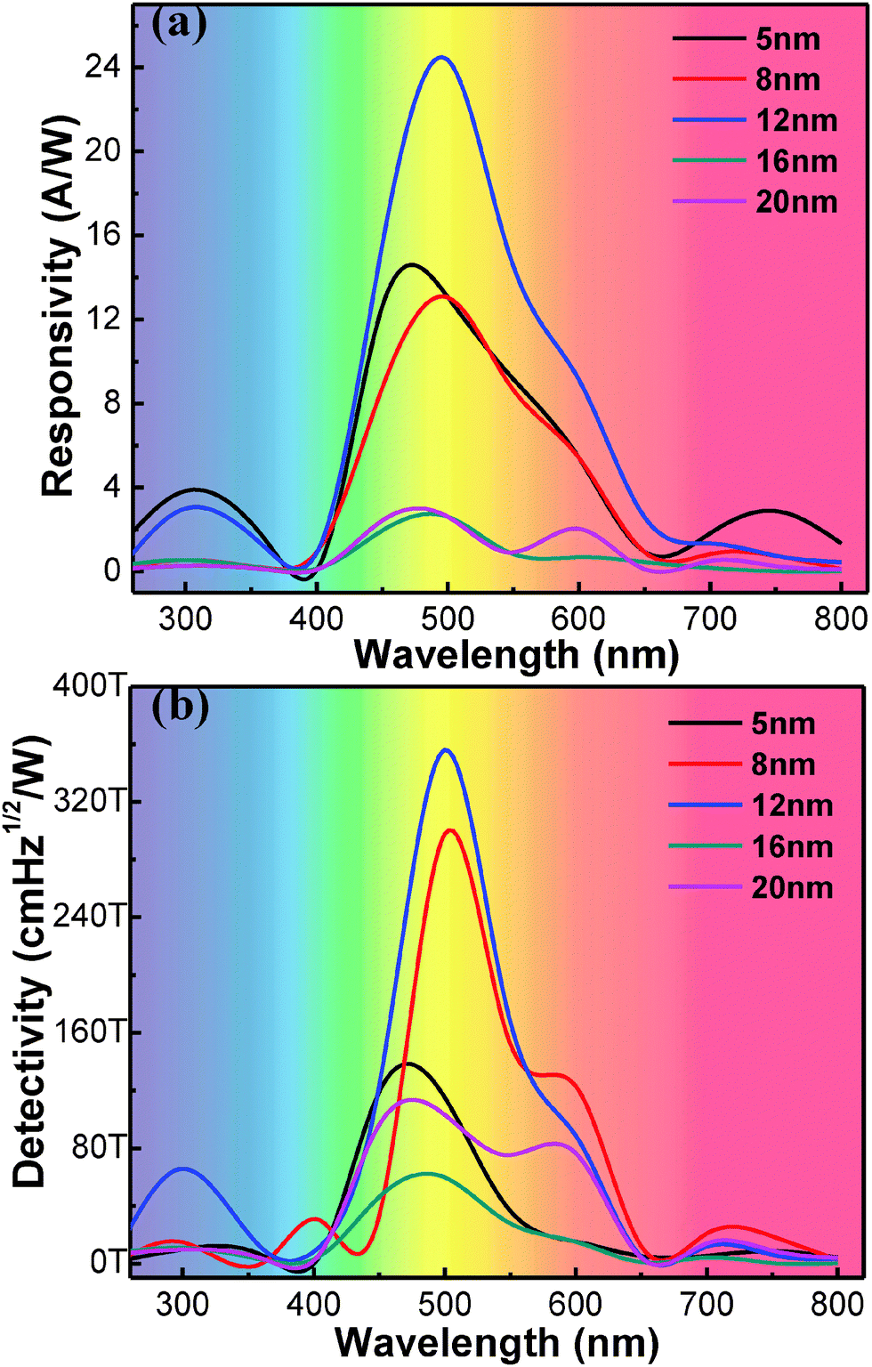 | ||
| Fig. 6 The responsivity (a) and detection sensitivity (b) of the as-fabricated detectors with the thicknesses of MoO3 ranging from 5 to 20 nm. | ||
Stability is of great importance to photoelectric devices. To characterize the device stability and repeatability, the as-fabricated photodetector was investigated under monochromatic light illumination through periodically and manually turning on/off the light source, as shown in Fig. 7. It is obvious that the photodetector exhibited good on/off switching properties with both 297 nm and 500 nm light. The on–off switching behaviour was preserved over multiple cycles, indicating the robustness and reproducibility of our photodetector. The response photocurrent was 1.5 μA under 500 nm light, which is larger than that of 0.8 μA under 297 nm light and the result is consistent with the detectivity performance. The rise and fall times were calculated to be less than 0.7 s and 0.6 s, as shown in Fig. S4 (ESI†). In addition, the illumination test was carried out to analyse the stability performance of the photodetector for three months, as shown in Fig. S5 (ESI†). The photocurrent remained 91.3% of the original value when kept illuminated under constant light intensity. The good stability performance of the device can be attributed to the MoO3 layer, which not only blocks the electrons for recombination, but also prevents air from penetrating into the perovskite.
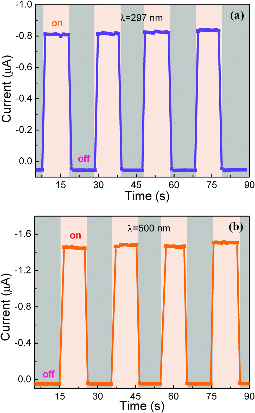 | ||
| Fig. 7 Photoelectric response of the device upon 297 nm (a) and 500 nm (b) light illumination measured for light-on and light-off conditions. | ||
4. Conclusions
In conclusion, high performance photodetectors with organolead iodide perovskite (CH3NH3PbI3) as an active absorption layer, a layer of gold modified by MoO3 as a positive electrode, and FTO/ZnO nanorods as a negative electrode are presented. The well aligned crystallized ZnO nanorods were synthesized by the water-bath method and the CH3NH3PbI3 nanoparticle layer was coated by a two-step method. One-dimensional ZnO nanorod/CH3NH3PbI3 can form a heterojunction structure and benefit the exciton separation and harvest, meanwhile the MoO3 inorganic metal oxide layer can both enhance the exciton transport and protect the organic perovskite layer. A high detectivity value of 3.56 × 1014 cm Hz1/2 W−1 and a high photo-responsivity value of 24.3 A W−1 were achieved using 500 nm light with 0 V external voltage. The self-powered perovskite photodetector is sensitive to a broadband wavelength from the ultraviolet light to entire visible light region. Furthermore, our photodetector exhibited very good repeatability and stability over a long period test.Acknowledgements
This work was supported by National Natural Science Foundation of China (Grant no. 51372075). Y. Wang and P. A. van Aken acknowledge funding from the European Union Seventh Framework Program (FP7/2007–2013) under grant agreement no. 312483 (ESTEEM2).References
- N. J. Jeon, J. H. Noh, W. S. Yang, Y. C. Kim, S. Ryu, J. Seo and S. II Seok, Nature, 2015, 517, 476 CrossRef CAS PubMed.
- M. I. Saidaminov, V. Adinolfi, R. Comin, A. L. Abdelhady, W. Peng, I. Dursun, M. Yuan, S. Hoogland, E. H. Sargent and O. M. Bakr, Nat. Commun., 2015, 6, 8724 CrossRef CAS PubMed.
- Z. Tan, R. S. Moghaddam, M. L. Lai, P. Docampo, R. Higler, F. Deschler, M. Price, A. Sadhanala, L. M. Pazos, D. Credgington, F. Hanusch, T. Bein, H. J. Snaith and R. H. Friend, Nat. Nanotechnol., 2014, 9, 687 CrossRef CAS PubMed.
- K. Chen and H. Tüysüz, Angew. Chem., Int. Ed., 2015, 54, 13806 CrossRef CAS PubMed.
- Y. Lee, J. Kwon, E. Hwang, C. H. Ra, W. J. Yoo, J. H. Ahn, J. H. Park and J. H. Cho, Adv. Mater., 2015, 27, 41 CrossRef CAS PubMed.
- W. Wang, M. O. Tadé and Z. Shao, Chem. Soc. Rev., 2015, 44, 5371 RSC.
- S. D. Stranks, G. E. Eperon, G. Grancini, C. Menelaou, M. J. P. Alcocer, T. Leijtens, L. M. Herz, A. Petrozza and H. J. Snaith, Science, 2013, 342, 341 CrossRef CAS PubMed.
- X. Gao, J. Li, J. Baker, Y. Hou, D. Guan, J. Chen and C. Yuan, Chem. Commun., 2014, 50, 6368 RSC.
- W. J. Yin, T. Shi and Y. Yan, Adv. Mater., 2014, 26, 4653 CrossRef CAS PubMed.
- L. Dou, Y. Yang, J. You, Z. Hong, W. Chang, G. Li and Y. Yang, Nat. Commun., 2014, 5, 5404 CrossRef CAS PubMed.
- H. Zhou, P. Gui, Q. Yu, J. Mei, H. Wang and G. Fang, J. Mater. Chem. C, 2015, 3, 990 RSC.
- S. Xu, Y. Qin, C. Xu, Y. Wei, R. Yang and Z. L. Wang, Nat. Nanotechnol., 2010, 5, 366 CrossRef CAS PubMed.
- P. N. Ni, C. X. Shan, S. P. Wang, X. Y. Liu and D. Z. Shen, J. Mater. Chem. C, 2013, 1, 4445 RSC.
- H. Shen, C. X. Shan, B. H. Li, B. Xuan and D. Z. Shen, Appl. Phys. Lett., 2013, 103, 232112 CrossRef.
- W. J. Nam, Z. Gray, J. Stayancho, V. Plotnikov, D. Kwon, S. Waggoner, D. V. Shenai-Khatkhate, M. Pickering, T. Okano, A. Compaan and S. J. Fonash, ECS Trans., 2015, 66, 275 CrossRef.
- H. S. Kim, C. R. Lee, J. H. Im, K. B. Lee, T. Moehl, A. Marchioro, S. J. Moon, R. Humphry-Baker, J. H. Yum, J. E. Moser, M. Grätzel and N. G. Park, Sci. Rep., 2012, 2, 501 Search PubMed.
- J. M. Ball, M. M. Lee, A. Hey and H. Snaith, Energy Environ. Sci., 2013, 6, 1739 CAS.
- Y. Guo, C. Liu, K. Inoue, K. Harano, H. Tanaka and E. Nakamura, J. Mater. Chem. A, 2014, 2, 13827 CAS.
- E. Voroshazi, B. Verreet, A. Buri, R. Muller, D. D. Nuzzo and P. Heremans, Org. Electron., 2011, 12, 736 CrossRef CAS.
- V. Shrotriya, G. Li, Y. Yao, C. W. Chu and Y. Yang, Appl. Phys. Lett., 2006, 88, 73508 CrossRef.
- E. L. Ratcliff, B. Zacher and N. R. Armstrong, J. Phys. Chem. Lett., 2011, 2, 1337 CrossRef CAS PubMed.
- J. Burschka, N. Pellet, S. Moon, R. Humphry-Baker, P. Gao, M. K. Nazeeruddin and M. Grätzel, Nature, 2013, 499, 316 CrossRef CAS PubMed.
- H. Yu, Z. Zhang, M. Han, X. Hao and F. Zhu, J. Am. Chem. Soc., 2005, 127, 2378 CrossRef CAS PubMed.
- X. Zou, H. Fan, Y. Tian and S. Yan, CrystEngComm, 2014, 16, 1149 RSC.
- J. H. Heo, S. H. Im, J. H. Noh, T. N. Mandal, C. Lim, J. A. Chang, Y. H. Lee, H. Kim, A. Sarkar, M. K. Nazeeruddin, M. Grätzel and S. Il Seok, Nat. Photonics, 2013, 7, 486 CrossRef CAS.
- T. Oku, Crystal Structures of CH3NH3PbI3 and Related Perovskite Compounds Used for Solar Cells, Solar Cells-New Approaches and Reviews, ed. L. A. Kosyachenko, InTech, ISBN: 78-953-51-2184-8, DOI: 10.5772/59284. Available from: http://www.intechopen.com/books/solar-cells-new-approaches-and-reviews/crystal-structures-of-ch3nh3pbi3-and-related-perovskite-compounds-used-for-solar-cells, 2015.
- S. S. Mali, C. S. Shim and C. K. Hong, Sci. Rep., 2015, 5, 11424 CrossRef PubMed.
- J. Meyer, S. Hamwi, M. Kröger, W. Kowalsky, T. Riedl and A. Kahn, Adv. Mater., 2012, 24, 5408 CrossRef CAS PubMed.
- X. Hu, L. Chen and Y. Chen, J. Phys. Chem. C, 2014, 118, 9930 CAS.
- X. Fan, C. Cui, G. Fang, J. Wang, S. Li, F. Cheng, H. Long and Y. Li, Adv. Funct. Mater., 2012, 22, 585 CrossRef CAS.
- X. Fan, G. Fang, P. Qin, N. Sun, N. Liu, Q. Zheng, F. Cheng, L. Yuan and X. Zhao, J. Phys. D: Appl. Phys., 2011, 44, 045101 CrossRef.
- X. Fan, G. Fang, S. Guo, N. Liu, H. Gao, P. Qin, S. Li, H. Long, Q. Zheng and X. Zhao, Nanoscale Res. Lett., 2011, 6, 546 CrossRef PubMed.
- L. E. Greene, M. Law, J. Goldberger, F. Kim, J. C. Johnson, Y. Zhang, R. J. Saykally and P. Yang, Angew. Chem., Int. Ed., 2003, 42, 3031 CrossRef CAS PubMed.
- L. E. Greene, M. Law, D. H. Tan, M. Montano, J. Goldberger, G. Somorjai and P. Yang, Nano Lett., 2005, 5, 1231 CrossRef CAS PubMed.
- N. K. Huu, D. Y. Son, I. H. Jang, C. R. Lee and N. G. Park, ACS Appl. Mater. Interfaces, 2013, 5, 1038 CAS.
- Y. Shen, X. Yan, Z. Bai, X. Zheng, Y. Liu, P. Lin, X. Chen and Y. Zhang, RSC Adv., 2015, 5, 5976 RSC.
- X. Gao, J. Li, J. Baker, Y. Hou, D. Guan, J. Chen and C. Yuan, Chem. Commun., 2014, 50, 6368–6371 RSC.
Footnotes |
| † Electronic supplementary information (ESI) available. See DOI: 10.1039/c6tc02097f |
| ‡ These authors contribute equally to this work. |
| This journal is © The Royal Society of Chemistry 2016 |