
 Open Access Article
 This Open Access Article is licensed under a
 Creative Commons Attribution 3.0 Unported Licence
High-performance non-volatile field-effect transistor memories using an amorphous oxide semiconductor and ferroelectric polymer†
Yu
Wang‡
a,
Takio
Kizu‡
b,
Lei
Song‡
a,
Yujia
Zhang
a,
Sai
Jiang
a,
Jun
Qian
a,
Qijing
Wang
a,
Yi
Shi
a,
Youdou
Zheng
a,
Toshihide
Nabatame
c,
Kazuhito
Tsukagoshi
*b and
Yun
Li
*a
aNational Laboratory of Solid State Microstructures, School of Electronic Science and Engineering, Collaborative Innovation Center of Advanced Microstructures, Nanjing University, Nanjing 210093, P. R. China. E-mail: yli@nju.edu.cn; yshi@nju.edu.cn
bInternational Center for Materials Nanoarchitectonics (WPI-MANA), National Institute for Materials Science (NIMS), 1-1 Namiki, Tsukuba, Ibaraki 305-0044, Japan. E-mail: TSUKAGOSHI.Kazuhito@nims.go.jp
cMANA Foundry and MANA Advanced Device Materials Group, National Institute for Materials Science (NIMS), Tsukuba, Ibaraki 305-0044, Japan
First published on 12th July 2016
Abstract
Ferroelectric field-effect transistors (Fe-FETs) are of great interest for a variety of non-volatile memory device applications. High-performance top-gate Fe-FET memories using ferroelectric polymers of poly(vinylidene fluoride–trifluoroethylene) (P(VDF–TrFE)) and the inorganic oxide of InSiO were fabricated. The extracted electron mobility was as high as 84.1 cm2 V−1 s−1 in a low-frequency state. The interfacial charge transfer between the P(VDF–TrFE) and InSiO during annealing of the P(VDF–TrFE) layer benefits improvement in the device performance. The results show the potential of our Fe-FET memories for next-generation electronics.
Introduction
Field-effect transistors (FETs) based on amorphous oxide semiconductors have been the focus of considerable interest for various applications, such as drivers for active-matrix displays with ultrahigh resolution.1–4 In recent years, hybrid ferroelectric non-volatile memories, which use oxide semiconductor materials and ferroelectric polymers as the conducting and dielectric layers, respectively, have been recognized as a promising strategy for the achievement of high electrical performance.5–7 Many studies involve amorphous oxide semiconductor ferroelectric FET memory.7–10 Among various ferroelectric polymer memories, those based on poly(vinylidene fluoride) and its copolymers are the most popular because of their easy solution processing, low annealing temperature, and excellent chemical stability.11,12 However, using poly(vinylidene fluoride–trifluoroethylene) (P(VDF–TrFE)) as an insulating layer for the ferroelectric transistors does not allow for high mobility. This issue also causes a slow charge accumulation process and storage speed.11 Therefore, a hybrid inorganic/organic structure using an amorphous oxide semiconductor is proposed to improve electrical performance. In our previous studies, we have investigated the relationship between the carrier mobility of the amorphous oxide semiconductor and interfacial charge carrier density.13,14 Carrier mobility can be improved with an increase in conducting charge density. For amorphous oxide semiconductor materials, electrical conduction is often the result of the existence of oxygen vacancies (VO) and interstitial metal atoms, which can act as electron donors and acceptors, respectively.15 InOx-based oxide materials are typical n-type oxide semiconductors, in which VO allows electrons to be available at the conduction band.15–21 In various studies involving InOx-based amorphous oxide semiconductors, doping of rare metals such as tin, zirconium, and gallium, always exists.20–25This study proposes a strategy for fabricating high-performance ferroelectric field-effect transistor (Fe-FET) memory with P(VDF–TrFE) as the dielectric layer and InSiO (In2O3/SiO2 = 90![[thin space (1/6-em)]](https://www.rsc.org/images/entities/char_2009.gif) :10 wt%) as the n-type semiconductor layer. InSiO is an n-type InOx-based oxide material without the second-time and rare-metal doping. The extracted field-effect mobility (μFET) is as high as 84.1 cm2 V−1 s−1 and was detected through capacitance measurement at low frequency, 200 Hz. The enhanced mobility is mainly dominated by the increase in charge carrier density, which is due to the existence of interfacial charge transfer from the P(VDF–TrFE) layer to the semiconducting channel. Our work reveals that Fe-FET memories using hybrid organic/inorganic structure are promising for next-generation electronics.
:10 wt%) as the n-type semiconductor layer. InSiO is an n-type InOx-based oxide material without the second-time and rare-metal doping. The extracted field-effect mobility (μFET) is as high as 84.1 cm2 V−1 s−1 and was detected through capacitance measurement at low frequency, 200 Hz. The enhanced mobility is mainly dominated by the increase in charge carrier density, which is due to the existence of interfacial charge transfer from the P(VDF–TrFE) layer to the semiconducting channel. Our work reveals that Fe-FET memories using hybrid organic/inorganic structure are promising for next-generation electronics.
Experimental
Fabrication of Fe-FET memories
Heavily-doped Si wafers with 250 nm-thick SiO2 on top were subsequently cleaned with acetone and isopropanol and then treated with UV-ozone. Ten nanometer-thick InSiO films were deposited on the wafer by DC magnetron sputtering using the InSiOx target, with a weight ratio of 90 to 10 between In2O3 and SiO2, through a shadow mask at room temperature. The channel width was set to 1000 μm. The InSiO films were annealed at 250 °C for 30 min under ambient atmosphere. Au (30 nm) was deposited by thermal evaporation through a shadow mask as the source and drain electrodes. Thereafter, 3 wt% P(VDF–TrFE) in a methyl ethyl ketone solution was spin-coated on the sample to obtain 240 nm-thick polycrystalline P(VDF–TrFE) films. The composition ratio between VDF and TrFE of copolymer P(VDF–TrFE) is 70:30. The sample was baked on a hotplate at 90 °C for 30 min and annealed at different temperatures (120 °C, 125 °C, 130 °C, and 140 °C) for 2 h. The entire process of the P(VDF–TrFE) layer fabrication was completed in a nitrogen glove box. Finally, 50 nm-thick Au was thermally evaporated on the P(VDF–TrFE) layer at a low speed of 0.01 nm s−1 through a shadow mask to form the top-gate electrodes.
Fabrication of Au/P(VDF–TrFE)/Au capacitors
A 25 nm-thick Au electrode was thermally evaporated on the substrate with 10 nm InSiO on top. Then, the P(VDF–TrFE) layer was spin-coated on the InSiO films. Finally, the Au (30 nm) electrode was deposited on the ferroelectric layer through the shadow mask. The structure is shown in the inset of Fig. S1 (ESI†).Fabrication of InSiO-based FETs
The heavily-doped Si wafer with 250 nm-thick SiO2 on top was used as the bottom gate and dielectric. An InSiO film with a 10-nm thickness was deposited on the SiO2 film by DC magnetron sputtering using the InSiOx target, and the weight ratio between In2O3 and SiO2 was 90 to 10. Then, the InSiO film was annealed at 250 °C for 30 min under ambient atmosphere. Finally, the source and drain electrodes of Au (30 nm) were deposited by thermal evaporation.Fabrication of FETs using PMMA as the dielectric
An InSiO film with a 10-nm thickness were deposited on the SiO2/Si substrate. After annealing for 30 min at 250 °C, the source and drain electrodes of Au (25 nm) were thermally deposited through a shadow mask. Then, 300 nm-thick PMMA was spin-coated to form the dielectric layer. Finally, the electrode, 30 nm-thick Au, was evaporated to fabricate the top-gate transistor.Memory characterizations
Electrical performance was characterized under ambient conditions using an Agilent 4156C semiconductor parameter analyzer. The Agilent 4980a LCR parameter analyzer and HIOKI LCR IM3533-01 meter were used for the C–V measurements.Results and discussion
Top-gate Fe-FET memories using P(VDF–TrFE) and InSiO as the dielectric and semiconductor layers, respectively, were fabricated (Fig. 1a). The channel length and width are 200 μm and 1000 μm, respectively. Fig. 1b presents a typical transfer curve as the gate voltage (VG) is swept from −30 V to 30 V and then back. From the slope of the transfer curve, electron mobility is estimated to be as high as 84.1 cm2 V−1 s−1 with the gate capacitance typically measured at a low-voltage-frequency state of 200 Hz. To estimate the carrier mobility, we selected the transfer curves when VG was swept in a reverse manner from 25 V to 5 V, in order to avoid the switching process of the ferroelectric layer. Although there is a large ferroelectric hysteresis in the curve, both forward and backward curves showed large mobility. To the best of our knowledge, this value represents the highest mobility for Fe-FETs using P(VDF–TrFE) and amorphous oxide semiconductors.7,8,26–29 The anticlockwise direction of the current hysteresis reveals that the charge-switching behavior is attributed to the dipolar polarization of P(VDF–TrFE) instead of charge trapping in the semiconductor layer.30 Thus, when VG is set to 0 V, our FET device exhibits two states with different electrical conductions, namely, the off and on states. Moreover, the on/off ratio and memory window obtained from the transfer curve were 106 and 27 V, respectively, which also denote good memory performance. Generally, a high carrier mobility in the semiconducting channel can lead to a fast operating speed, which is an important parameter for the evaluation of FET memory operation.31 We performed a frequency response measurement to represent the “reading” process (Fig. 1c). The measurement shows a negligible decrease until the frequency increases to 104 Hz, indicating a short “reading” time of approximately 0.1 ms. Moreover, the abrupt switching of the drain current reveals a fast pulse response to the VG pulse, which represents the “programming” process (Fig. 1d and e). The pulse responses, as measured by adding a voltage pulse, show short delay times of approximately 0.2 and 0.3 ms from the off state to the on state and from the on state to the off state, respectively (Fig. 1d and e). The sub-millisecond delay time indicates a fast switching behavior close to the speed of the polarization switching of P(VDF–TrFE).32,33 In addition, the sustainability of a memory operation is also an important feature for the industry. Fig. 1f shows the retention measurements of on and off currents for 106 s, indicating a good non-volatile property of our Fe-FET memories. A slight increase in the on current was observed from ∼105 s, which can be attributed to the enhancement of the interaction between P(VDF–TrFE) and InSiO by Joule's heat. Besides, the devices can maintain a high on/off ratio of >105 after cycling 1000 times (see ESI,† Fig. S2).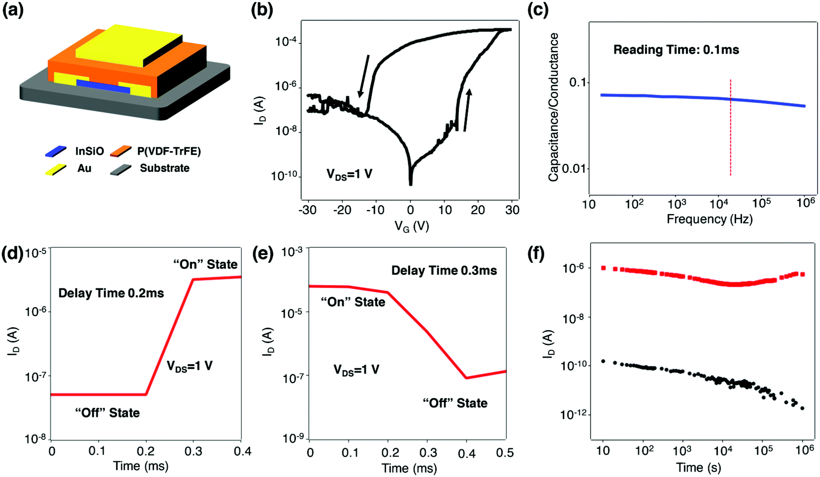 | ||
| Fig. 1 (a) Schematic of a Fe-FET with a top-gate top-contact structure. (b) Typical transfer curve of the Fe-FET. For InSiO channel, after sputtering the InSiO film, the film was thermally annealed at 250 °C. (c) Dependence of capacitance divided by the channel conductance on VG frequency. (d and e) Pulse responses of the Fe-FET memory from the off state to the on state and from the on state to the off state, respectively. (f) Shows that the retention measurements of on and off currents, indicating a good non-volatile property of our Fe-FET memories. | ||
As mentioned previously, the FET carrier mobility of our hybrid-memories is estimated in the linear region using the following equation:
 | (1) |
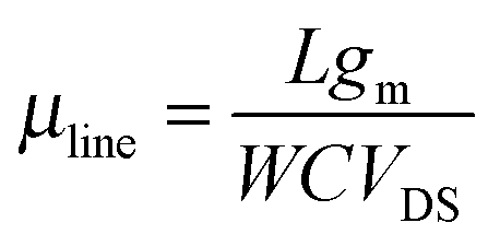
In our previous study, InSiO-based FETs using SiO2 as the dielectric layer exhibited a significantly low carrier mobility of 7.7 cm2 V−1 s−1 (the channel length and width were 350 μm and 1000 μm, respectively) when the ratio between In2O3 and SiO2 was similar to that in the present Fe-FETs (also see ESI,† Fig. S3).20 Thus, we consider that the significant enhancement in the field-effect mobility of our Fe-FETs should be attributed to the interfacial effect between InSiO and P(VDF–TrFE). The ferroelectric property of P(VDF–TrFE) stems from the flexibility of the molecular axis, enabling change in the dipole moment direction. Ferroelectricity originates from the crystalline phase. Thus, the annealing treatment of P(VDF–TrFE) is necessary to increase the degree of crystallinity.36,37 Therefore, we first examined the surface property of P(VDF–TrFE) under different annealing temperatures by using atomic force microscopy (AFM) measurements. Fig. 2a and b show the morphology and phase images of the P(VDF–TrFE) thin film without annealing treatment, respectively, and both exhibit an amorphous phase. The glass transition temperature of P(VDF–TrFE) is 118 °C.31 Therefore, P(VDF–TrFE) film annealed at a temperature above this value forms highly crystalline phases with needle-like grains that enhance the ferroelectric property (Fig. 2c–h). Moreover, the grain sizes and surface roughness increase with the annealing temperature (Fig. 2k). As the annealing temperature further increases to the melting point of P(VDF–TrFE) (140 °C),31 the film mainly exhibits an amorphous phase (Fig. 2i and j).
 | ||
| Fig. 2 (a–j) AFM morphology and phase images of P(VDF–TrFE) films deposited on InSiO layers with different annealing temperatures. (k) Root-mean-square roughness values and grain sizes of P(VDF–TrFE) films annealed at different temperatures. | ||
Subsequently, we investigated the electrical performances of our Fe-FETs under different annealing conditions. We fabricated 10 memories for the P(VDF–TrFE) layers annealed at different temperatures. The estimated FET mobility and memory window of the un-annealed memory are 0.79 ± 0.59 cm2 V−1 s−1 and 6 ± 1 V, respectively (Fig. 3a). For the annealed sample, the carrier mobility and memory window were enhanced from 120 °C to 130 °C (Fig. 3b–d). In particular, the device annealed at 130 °C yielded an enhanced carrier mobility of 75.40 ± 9.54 cm2 V−1 s−1 and a large memory window of 21 ± 6 V. The highest carrier mobility obtained was 84.1 cm2 V−1 s−1. Moreover, when the annealing temperature increased to the melting point of P(VDF–TrFE) at 140 °C, the carrier mobility and memory window decreased to 27.90 ± 5.42 cm2 V−1 s−1 and 4 ± 2 V, respectively (Fig. 3e). Fig. 3f and Table S1 (ESI†) summarize the carrier mobility, on/off ratio, and memory window under different voltage frequencies for the capacitance measurements. In particular, the capacitance measurements showed a similar change in carrier mobility at a low frequency of 200 Hz and quasi-static frequency of 0.1 Hz. Consequently, the results strongly imply that the interfacial effect that exists at the ferroelectric/InSiO interface during the annealing treatment can improve the electrical characteristics of Fe-FETs.
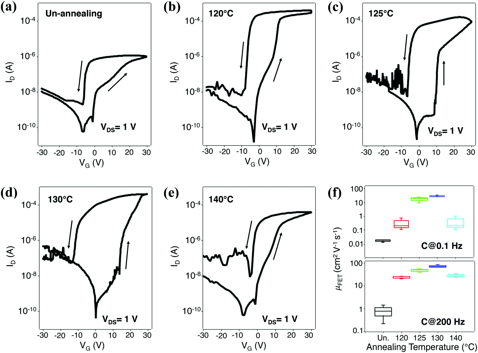 | ||
| Fig. 3 (a–e) Transfer characteristics of Fe-FETs with different annealing conditions for P(VDF–TrFE). (f) Summary of the values of carrier mobility at different annealing temperatures. | ||
For the InSiO semiconducting films, the conduction band where the electrons are transported is formed by unoccupied indium s orbitals, and the valence band is formed by fully occupied oxygen 2p orbitals.38 The In atoms with dangling bonds, that is, VO, have energy levels near the conduction band edge; these states act as shallow donors. Thus, the fully oxidized In atoms are regarded as insulators, and the In atoms with VO are utilized as conductors.38 At the P(VDF–TrFE)/InSiO interface, charge transfer occurs, increasing the charge density (see ESI,† Fig. S4). Consequently, the polarization-bound charges in P(VDF–TrFE) will be screened by the mobile charges in InSiO, resulting in a charge accumulation layer at the surface of the semiconductor layer.39 Therefore, the charge concentration in InSiO is increased, leading to a shift of the zero-gate-bias Fermi level toward the conduction band and to an enhancement in the electrical performance. In order to avoid the influence of the negative voltage on the charge distribution in the semiconductor channel, we examined the initial drain currents (VG = 0 V) of as-fabricated Fe-FETs using P(VDF–TrFE) under different annealing conditions with the same structure to verify the results. The values of the initial drain currents were extracted from the transfer curves at the starting point of VG sweeping (Fig. 4a–e). The high temperature applied during the annealing process can enhance the interfacial interaction between P(VDF–TrFE) and InSiO, leading to a high charge concentration in the conducting channel. As shown in Fig. 4f, the initial drain current increases from 10−10 A for the unannealed device to 10−6 A for the annealed device at 130 °C. The decrease in initial drain current for the device annealed at 140 °C is due to the loss of crystallinity in P(VDF–TrFE). Moreover, the change in the initial drain current along with the annealing temperature is similar to that of carrier mobility, as shown in Fig. 3f. This indicates that the enhancement of electrical performance should be devoted to the interfacial interaction between P(VDF–TrFE) and InSiO. Finally, we further confirm this interfacial effect by fabricating top-gate devices using poly(methyl methacrylate) (PMMA) as the top-gate dielectric (see ESI,† Fig. S5). A typical transfer curve exhibited a value carrier mobility (10.1 cm2 V−1 s−1) similar to that of FETs using SiO2 as the bottom-gate dielectric (9.1 cm2 V−1 s−1); and both are significantly lower than that of devices using annealed P(VDF–TrFE).
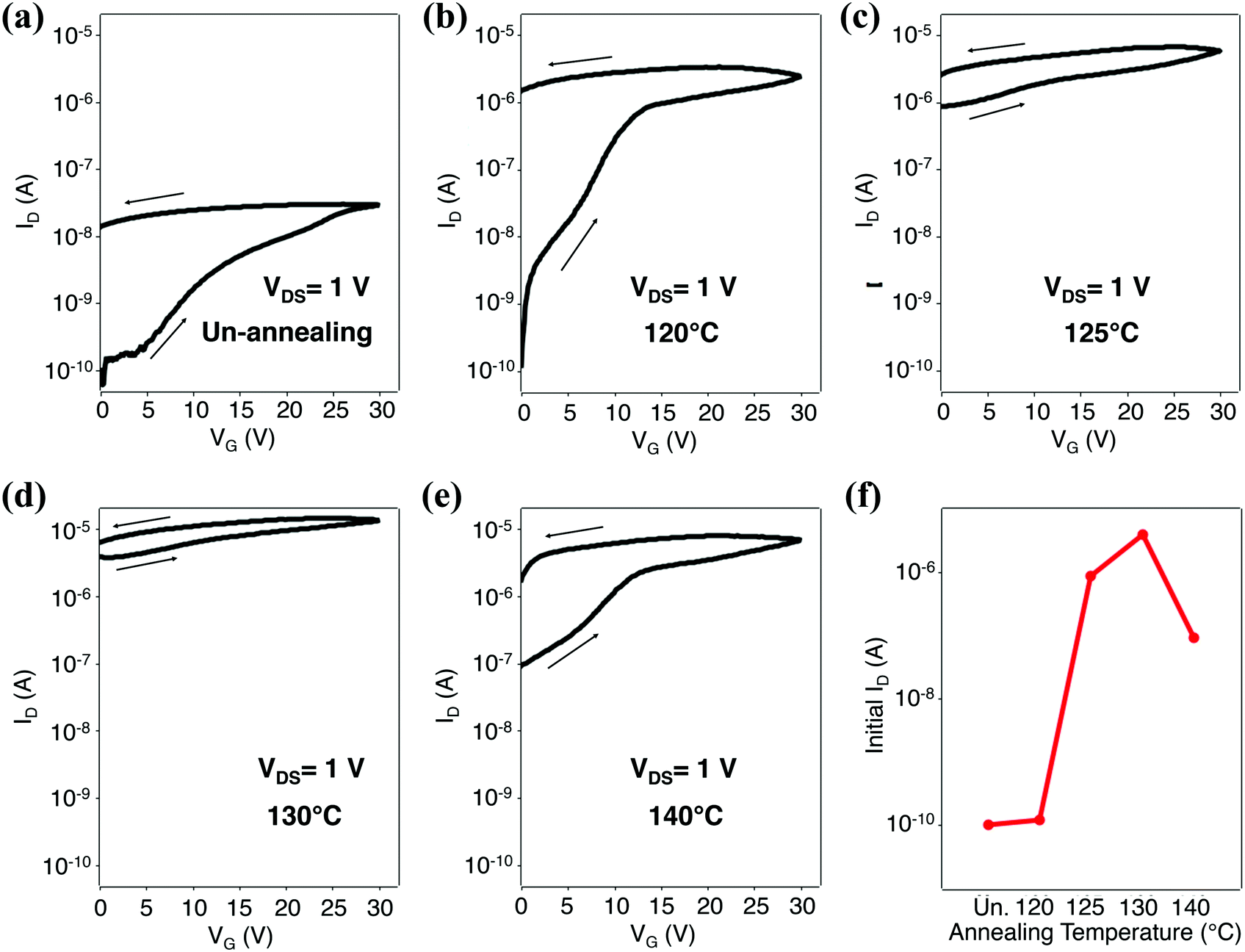 | ||
| Fig. 4 To avoid the impact of the negative voltage on charge distribution in semiconductor channel, we examined the initial drain currents (VG = 0 V) of as-fabricated Fe-FETs using P(VDF–TrFE) with different annealing conditions under the same structure. (a–e) Transfer characteristics of Fe-FETs with different annealing temperatures for P(VDF–TrFE), with VG swept from 0 V to 30 V and then backwards. (f) Initial drain currents at the starting point (VG = 0 V) of the VG sweeping process for Fe-FETs with different annealing temperatures for P(VDF–TrFE). | ||
Conclusions
In summary, we fabricated a high-performance Fe-FET memory using InSiO and P(VDF–TrFE) as the semiconductor and dielectric layers, respectively. The interfacial interaction between the P(VDF–TrFE) and InSiO layers during the annealing treatment of P(VDF–TrFE) led to an increase in charge density in the conducting channel. A high mobility of 84.1 cm2 V−1 s−1 in the low-frequency state was obtained. Based on the enhanced mobility, a fast operating speed was achieved for our Fe-FETs.Acknowledgements
This study is supported partially by 973 projects (No. 2013CBA01600 and 2013CB932900), NSFC (No. 61574074 and 61306021), NSFJS (No. BK20130579), Grants-in-Aid for Scientific Research (No. 15H03568 and 26790051), and Open Partnership Joint Projects of NSFC-JSPS Bilateral Joint Research Projects (No. 61511140098).References
- T. Kamiya, K. Nomura and H. Hosono, Sci. Technol. Adv. Mater., 2010, 11, 044305 CrossRef.
- J. Raja, K. Jang, C.-P-T. Nguyen, N. Balaji, S. Chatterjee and J. Yi, IEEE Electron Device Lett., 2014, 35, 756 CrossRef CAS.
- J.-S. Park, T.-W. Kim, D. Stryakhilev, J.-S. Lee, S.-G. An, Y.-S. Pyo, D.-B. Lee, Y. G. Mo, D.-U. Jin and H. K. Chung, Appl. Phys. Lett., 2009, 95, 013503 CrossRef.
- M. Kaneyasu, H. Miyake, T. Nishi, Y. Hirakata, J. Koyama, R. Sato, M. Sakakura and S. Yamazaki, ECS Trans., 2011, 37, 89 CAS.
- J. F. Wager and R. Hoffman, IEEE Spectrum, 2011, 48, 42 CrossRef.
- S. Aikawa, T. Nabatame and K. Tsukagoshi, Appl. Phys. Lett., 2013, 103, 172105 CrossRef.
- M. A. Khan, J. A. Caraveo-Frescas and H. N. Alshareef, Org. Electron., 2014, 16, 9 CrossRef.
- G. H. Gelinck, B. Cobb, A. J. J. M. van Breemen and K. Myny, Semicond. Sci. Technol., 2015, 30, 074003 CrossRef.
- A. Houachtia, P. Alcouffe, G. Boiteux, G. Seytre, J. F. Gerard and A. Serghei, Nano Lett., 2015, 15, 4311 CrossRef CAS PubMed.
- N. H. Van, J. H. Lee, D. Whang and D. J. Kang, Nanoscale, 2015, 7, 11660 RSC.
- R. C. G. Naber, K. Asadi, P. W. M. Blom, D. M. de Leeuw and B. de Boer, Adv. Mater., 2010, 22, 933 CrossRef CAS PubMed.
- Y. J. Park, I.-S. Bae, S. J. Kang, J. Chang and C. Park, IEEE Trans. Dielectr. Electr. Insul., 2010, 17, 1135 CrossRef CAS.
- M.-F. Lin, X. Gao, N. Mitoma, T. Kizu, W. Ou-Yang, S. Aikawa, T. Nabatame and K. Tsukagoshi, AIP Adv., 2015, 5, 017116 CrossRef.
- N. Mitoma, S. Aikawa, W. Ouyang, X. Gao, T. Kizu, M.-F. Lin, A. Fujiwara, T. Nabatame and K. Tsukagoshi, Appl. Phys. Lett., 2015, 106, 042106 CrossRef.
- E. Fortunato, P. Barquinha and R. Martins, Adv. Mater., 2012, 24, 2945 CrossRef CAS PubMed.
- S. Tomai, M. Nishimura, M. Itose, M. Matsuura, M. Kasami, S. Matsuzaki, H. Kawashima, F. Utsuno and K. Yano, Jpn. J. Appl. Phys., 2012, 51, 03CB01 CrossRef.
- T. Maruyama and T. Tago, Appl. Phys. Lett., 1994, 64, 1395 CrossRef CAS.
- H. Kumomi, S. Yaginuma, H. Omura, A. Goyal, A. Sato, M. Watanabe, M. Shimada, N. Kaji, K. Takahashi, M. Ofuji, T. Watanabe, N. Itagaki, H. Shimizu, K. Abe, Y. Tateishi, H. Yabuta, T. Iwasaki, R. Hayashi, T. Aiba and M. Sano, J. Disp. Technol., 2009, 5, 531 CrossRef CAS.
- S. Aikawa, P. Darmawan, K. Yanagisawa, T. Nabatame, Y. Abe and K. Tsukagoshi, Appl. Phys. Lett., 2013, 102, 102101 CrossRef.
- T. Kizu, S. Aikawa, N. Mitoma, M. Shimizu, X. Gao, M.-F. Lin, T. Nabatame and K. Tsukagoshi, Appl. Phys. Lett., 2014, 104, 152103 CrossRef.
- K. Nomura, H. Ohta, A. Takagi, T. Kamiya, M. Hirano and H. Hosono, Nature, 2004, 432, 488 CrossRef CAS PubMed.
- G. Goncalves, P. Barquinha, L. Pereira, N. Franco, E. Alves, R. Martins and E. Fortunato, Electrochem. Solid-State Lett., 2010, 13, 20 CrossRef.
- J. W. Hennek, J. Smith, A. Yan, M.-G. Kim, W. Zhao, V. P. Dravid, A. Facchetti and T. J. Marks, J. Am. Chem. Soc., 2013, 135, 10729 CrossRef CAS PubMed.
- H. Li, M. Qu and Q. Zhang, IEEE Electron Device Lett., 2013, 34, 1268 CrossRef CAS.
- J.-S. Park, K. S. Kim, Y. G. Park, Y. G. Mo, H. D. Kim and J. K. Jeong, Adv. Mater., 2009, 21, 329 CrossRef CAS.
- N. M. Triet, T. Q. Trung, N. T. D. Hien, S. Siddiqui, D.-I. Kim, J. C. Lee and N.-E. Lee, Nano Res., 2015, 8, 3421 CrossRef.
- S.-M. Yoon, S. Yang, C. Byun, S.-H. K. Park, D.-H. Cho, S.-W. Jung, O.-S. Kwon and C.-S. Hwang, Adv. Funct. Mater., 2010, 20, 921 CrossRef CAS.
- G.-G. Lee, E. Tokumitsu, S.-M. Yoon, Y. Fujisaki, J.-W. Yoon and H. Ishiwara, Appl. Phys. Lett., 2011, 99, 012901 CrossRef.
- S.-M. Yoon, S. Yang, C.-W. Byun, S.-W. Jung, M.-K. Ryu, S.-H. K. Park, B. Kim, H. Oh, C.-S. Hwang and B.-G. Yu, Semicond. Sci. Technol., 2011, 26, 034007 CrossRef.
- J. J. Brondijk, K. Asadi, P. W. M. Blom and D. M. de Leeuw, J. Polym. Sci., Part B: Polym. Phys., 2012, 50, 47 CrossRef CAS.
- H. B. Sun, Q. Wang, Y. Li, Y. F. Lin, Y. Wang, Y. Yin, Y. Xu, C. Liu, K. Tsukagoshi, L. Pan, X. Wang, Z. Hu and Y. Shi, Sci. Rep., 2014, 4, 7227 CrossRef CAS PubMed.
- T. Furukawa, T. Nakajima and Y. Takahashi, IEEE Xplore, 2006, 13, 1120 CAS.
- S. Horiuchi and Y. Tokura, Nat. Mater., 2008, 7, 357 CrossRef CAS PubMed.
- C. Wang, W. Y. Lee, D. Kong, R. Pfattner, G. Schweicher, R. Nakajima, C. Lu, J. Mei, T. H. Lee, H. C. Wu, J. Lopez, Y. Diao, X. Gu, S. Himmelberger, W. Niu, J. R. Matthews, M. He, A. Salleo, Y. Nishi and Z. Bao, Sci. Rep., 2015, 5, 17849 CrossRef CAS PubMed.
- E. G. Bittle, J. I. Basham, T. N. Jackson, O. D. Jurchescu and D. J. Gundlach, Nat. Commun., 2016, 7, 10908 CrossRef CAS PubMed.
- Y. Li, C. Liu, L. Pan, L. Pu, H. Sirringhaus and Y. Shi, Appl. Phys. Lett., 2011, 98, 173306 CrossRef.
- D. Y. Kusuma and P. S. Lee, Adv. Mater., 2012, 24, 4163 CrossRef CAS PubMed.
- N. Mitoma, S. Aikawa, X. Gao, T. Kizu, M. Shimizu, M.-F. Lin, T. Nabatame and K. Tsukagoshi, Appl. Phys. Lett., 2014, 104, 102103 CrossRef.
- M. W. J. Prins, S. E. Zinnemers, J. F. M. Cillessen and J. B. Giesbers, Appl. Phys. Lett., 1997, 70, 458 CrossRef CAS.
Footnotes |
| † Electronic supplementary information (ESI) available. See DOI: 10.1039/c6tc01768a |
| ‡ These authors contributed equally to this work. |
| This journal is © The Royal Society of Chemistry 2016 |