
 Open Access Article
 This Open Access Article is licensed under a
 Creative Commons Attribution 3.0 Unported Licence
Colloidal AgSbSe2 nanocrystals: surface analysis, electronic doping and processing into thermoelectric nanomaterials†
Yu
Liu
a,
Doris
Cadavid
*a,
Maria
Ibáñez
bc,
Jonathan
De Roo
d,
Silvia
Ortega
 a,
Oleksandr
Dobrozhan
a,
Maksym
V. Kovalenko
bc and
Andreu
Cabot
*ae
a,
Oleksandr
Dobrozhan
a,
Maksym
V. Kovalenko
bc and
Andreu
Cabot
*ae
aCatalonia Institute for Energy Research-IREC, Jardins de les Dones de Negre 1, 08930, Sant Adrià del Besos, Spain. E-mail: dcadavid@irec.cat; acabot@irec.cat
bInstitute of Inorganic Chemistry, Department of Chemistry and Applied Biosciences, ETH Zürich, CH-8093, Switzerland
cEmpa-Swiss Federal Laboratories for Materials Science and Technology, Dübendorf, CH-8600, Switzerland
dGhent University, Department of Inorganic and Physical Chemistry, Krijgslaan 281 S3, 9000 Gent, Belgium
eInstitució Catalana de Recerca i Estudis Avançats – ICREA, 08010 Barcelona, Spain
First published on 13th April 2016
Abstract
We present a high-yield and scalable colloidal synthesis to produce monodisperse AgSbSe2 nanocrystals (NCs). Using nuclear magnetic resonance (NMR) spectroscopy, we characterized the NC surface chemistry and demonstrate the presence of surfactants in dynamic exchange, which controls the NC growth mechanism. In addition, these NCs were electronically doped by introducing small amounts of bismuth. To demonstrate the technological potential of such processed material, after ligand removal by means of NaNH2, AgSbSe2 NCs were used as building blocks to produce thermoelectric (TE) nanomaterials. A preliminary optimization of the doping concentration resulted in a thermoelectric figure of merit (ZT) of 1.1 at 640 K, which is comparable to the best ZT values obtained with a Pb- and Te-free material in this middle temperature range, with the additional advantage of the high versatility and low cost associated with solution processing technologies.
1. Introduction
I–V–VI2 semiconductors, particularly AgSbSe2, show very attractive and yet to be exploited functional properties. AgSbSe2, with a rock-salt crystal structure, is highly suitable, for instance, as a phase change recording material in rewritable optical memories due to drastic resistance drop upon crystallization from an amorphous state.1–6 Within the AgSbSe2 structure, Ag and Sb are generally assumed to randomly occupy the Na sites of the NaCl-type lattice,7–10 which is consistent with ab initio calculations showing the total energies of the various ordered structures to be very close, thus allowing the presence of a significant density of disorder defects and mixed phases. A careful structural characterization has shown domains of ordering, not only in AgSbSe2,11 but also in the related AgSbTe2,12 correlating well with calculations showing a rhombohedral ordering to be the most energetically favorable in AgSbSe2.13 Atomic ordering within the AgSbSe2 crystal has a significant impact on the electronic structure near the band gap, which dominates the electronic properties14 and provides the material with ferroelectric properties.11AgSbSe2 is a narrow, indirect band-gap semiconductor (0.03–0.10 eV) showing p-type conductivity.15 However, an apparent optical bandgap of 0.6–1.1 eV2,15–18 and a high optical absorption coefficient (104 cm−1) have also motivated the use of AgSbSe2 for photovoltaic applications.2,17,19–21
The AgSbSe2 band structure is characterized by a multi-peak valence band maximum, which potentially results in a high effective mass for holes and thus a high Seebeck coefficient. In addition, AgSbSe2 features a strong anharmonic bonding arrangement associated with the Sb 5s2 lone pair, which translates into strong phonon–phonon interactions that reduce the lattice thermal conductivity to values close to the amorphous limit. This intrinsically low thermal conductivity and the appropriate electronic band structure make AgSbSe2 and AgSbTe2 promising candidates for TE applications in the intermediate temperature range (500–700 K).16,22–28 While AgSbTe2 exhibits higher electrical conductivity, and its nanostructured alloys with GeTe (TAGS)29 and PbTe (LAST-m)30 are well known for their remarkable ZT values, AgSbSe2 is advantageous in terms of thermal stability, abundance of constituting elements and cost. Bulk AgSbSe2 is typically produced by the solid state reaction of its highly purified elements at temperatures above 1000 K. A relatively large variety of extrinsic electronic dopants, introduced as pure elements in the reaction mixture, have been tested, including the substitution of Sb3+ by monovalent Na+,28 divalent Pb2+,16 Zn2+,23 Sn2+,24 Cd2+,26 Mg2+,27 Ba2+,27 and peculiarly by trivalent Bi3+.16 Extrinsic dopants can also introduce additional disorder and point defect scattering reducing the material thermal conductivity. In some cases, e.g. Na+, Zn2+ and Ba2+ can also introduce nanoprecipitates with modified stoichiometry, e.g. Na-rich AgSbSe2 or even of secondary phases, e.g. ZnSe and BaSe3, which further reduce thermal conductivity and allow reaching ZT values of up to ∼1.1.23,27 Besides, intrinsic doping strategies based on tuning the material stoichiometry by modifying, for instance, the Sb content25 and reaching ZT values of up to ∼1 have also been tested by solid state reaction methods.
The preparation of AgSbSe2 with controlled properties by means of solution processing methods is especially appealing to investigate the structural and compositional dependent functional properties, optimize the material for relevant applications and develop high performance cost-effective products. In particular, the availability of AgSbSe2 NCs with tuned size, shape, composition and phase would allow high density data storage systems, cost-effective photovoltaic devices and high performance thermoelectric modules to be produced by highly versatile, low-cost, high-throughput and high-yield solution-based bottom-up technologies.31–36 However, to the best of our knowledge, no synthesis protocol to produce colloidal AgSbSe2 NCs is currently available.
Here, we detail the first colloidal synthesis of monodisperse AgSbSe2 NCs on the gram scale, determine the NC surface composition by NMR analysis and demonstrate the possibility of electronically doping this material with controlled amounts of bismuth. Finally, we elaborate upon a procedure to remove organic ligands and demonstrate the suitability of these NCs to produce high performance thermoelectric nanomaterials.
2. Experimental section
2.1. Chemicals and solvents
Silver nitrate (AgNO3, ≥99%), antimony(III) chloride (SbCl3, 99%), selenium powder (Se, 99.5%), bismuth(III) acetate (Bi(CH3CO2)3, >99.99%), sodium amide (NaNH2, 95%), 1-dodecanethiol (DDT, ≥98%), oleic acid (OA, 90%), 1-octadecene (ODE, 90%), and oleylamine (OLA, 70%) were purchased from Sigma-Aldrich. Analytical grade acetone and chloroform were obtained from various sources. All chemicals were used as received without further purification. Syntheses were carried out using a standard vacuum/dry argon Schlenk line.2.2. Selenium precursor stock solution
A 0.5 M selenium stock solution was prepared by dissolving selenium powder (1.5792 g, 20 mmol) in 20 ml OLA and 20 ml DDT at room temperature, cycled between vacuum and argon to remove the oxygen in the flask, and then stirred under an Ar atmosphere until Se powder was completely dissolved.2.3. Synthesis of AgSbSe2 NCs
In a typical synthesis, AgNO3 (5 mmol, 0.849 g), SbCl3 (5 mmol, 1.141 g), 70 ml OLA and 10 ml OA were mixed in a 250 ml three-neck flask at room temperature under magnetic stirring for 30 min in order to remove low boiling point impurities. Afterwards, the solution was maintained at 80 °C under vacuum for 60 min. At around 70 °C the solution became yellowish and changed from ivory yellow to yellowish-brown during the time at 80 °C. Then the solution was heated to 120 °C for another 10 min under vacuum. After these steps, argon was introduced and the reaction was rapidly heated to 220 °C. At this temperature, 20 ml of a 0.5 M selenium solution were quickly injected. After injection, the color of the solution changed immediately from yellowish-brown to dark brown, indicating the NC nucleation. NCs were allowed to grow for 30 min at 220 °C. Afterwards, the colloidal solution was rapidly cooled to room temperature through a water bath. The resultant dark brown solution was cleaned by centrifugation at 6000 rpm for 5 min using chloroform as a solvent and acetone as a non-solvent.2.4. Synthesis of Bi-doped AgSbSe2 NCs
Bi-doped AgSbSe2 NCs were synthesized by using the same process as the pristine NCs, but replacing the desired amount of SbCl3 by Bi(CH3CO2)3. To produce AgSb0.98Bi0.02Se2, the precursor molar ratio was SbCl3/Bi(CH3CO2)3 = 0.98/0.02 (4.9 mmol/0.1 mmol).2.5. Nuclear magnetic resonance (NMR)
NMR measurements were recorded on a Bruker Avance III HD spectrometer operating at a 1H frequency of 500.26 MHz and equipped with a BBFO-Z probe. The sample temperature was set to 298.2 K. One dimensional (1D) 1H and 2D NOESY (Nuclear Overhauser Effect Spectroscopy) spectra were acquired using standard pulse sequences from the Bruker library. For the quantitative 1D 1H measurements, 64k data points were sampled with the spectral width set to 20 ppm and a relaxation delay of 30 s. The NOESY mixing time was set to 300 ms and 4096 data points in the direct dimension and 512 data points in the indirect dimension were sampled, with the spectral width set to 12 ppm. Diffusion measurements (2D DOSY) were performed using a double stimulated echo sequence for convection compensation and with monopolar gradient pulses.37 Smoothed rectangle gradient pulse shapes were used throughout. The gradient strength was varied quadratically from 2–95% of the probe's maximum value in 64 increments, with the gradient pulse duration and diffusion delay optimized to ensure a final attenuation of the signal in the final increment of less than 10% relative to the first increment. For 2D processing, the spectra were zero filled until a 4096–2048 real data matrix. Before Fourier transformation, the 2D spectra were multiplied with a squared cosine bell function in both dimensions, and the 1D spectra were multiplied with an exponential window function. Concentrations were obtained using the Digital ERETIC method, as provided in the standard software of Bruker. The diffusion coefficients were obtained by fitting the appropriate Stejskal–Tanner equation to the signal intensity decay.382.6. NC ligand displacement (LD)
NaNH2 was used to displace organic ligands from the AgSbSe2 and AgSb0.98Bi0.02Se2 NC surface. In a typical procedure, AgSbSe2 NCs (500 mg) were dispersed in 15 ml of chloroform and mixed at room temperature with 5 ml of NaNH2 solution (0.02 M) in methanol. The solution was shaken for 1–2 min to displace the organic ligands attached to the NC surface. This process was repeated twice. Afterward, NCs were precipitated by centrifugation and they were thoroughly purified using chloroform and acetone to remove the remaining organic surfactants and excess NaNH2. Finally, AgSbSe2 NCs were precipitated and dried under vacuum to obtain a fine nanopowder.2.7. Bulk nanomaterials
AgSbSe2 and AgSb0.98Bi0.02Se2 nanopowders obtained from drying 15 nm NCs were loaded into graphite dies and compacted into pellets (Ø10 mm × ∼1.5 mm) in an Ar atmosphere using a custom-made hot press. The process temperature was maintained between 350 °C and 360 °C for 30 min and the pressure was set to 70 MPa. In this system, heat is provided by an induction coil operated in the RF range applied directly to a graphite die, which acts as a susceptor, resulting in a heating ramp of about 20 °C per second. The density of the pressed pellets was always higher than 93% of their theoretical value.2.8. Structural and chemical characterization
X-ray diffraction analyses were carried out on a Bruker AXS D8 ADVANCE X-ray diffractometer using Cu-Kα radiation (λ = 0.15406 Å). The size and shape of initial NCs were examined by transmission electron microscopy (TEM) using a ZEISS LIBRA 120, operating at 120 kV. High resolution TEM (HRTEM) images were recorded using a JEOL JEM-2200FS microscope operated at 200 kV. For TEM analysis colloidal nanoparticles in chloroform were supported by drop-casting the solution on a carbon-coated copper grid at room temperature and ambient atmosphere. For HRTEM characterization of the pellets, we manually ground a piece of the measured pellet and mixed the obtained powder with TCE (tetrachloroethylene). The powder suspension was drop casted onto a carbon coated copper grid at room temperature and ambient atmosphere. Field-emission scanning electron microscopy (SEM) was carried out on an Auriga Zeiss at 5.0 kV. Quantitative elemental analysis was made by means of an energy dispersive X-ray spectroscopy (EDX) detector attached to a SEM.2.9. Thermoelectric measurements
Seebeck coefficient was measured by using a static DC method. Electrical resistivity data were obtained by a standard four-probe method. Both the Seebeck coefficient and the electrical resistivity were measured simultaneously in a LSR-3 LINSEIS system in the range between room temperature and 700 K, under a helium atmosphere. XFA 600 xenon flash equipment was used to determine the thermal diffusivities of the samples. The carrier concentration and mobility were measured using the Hall measurement system (PPMS-9T, Quantum Design Inc., USA) at room temperature under a magnetic field of 2 T. The thermal conductivity was calculated using κ = λCpρ, where λ is the thermal diffusivity, Cp is the heat capacity, and ρ is the mass density of the specimen. The specific heat capacity (Cp) was measured by means of a differential scanning calorimetry method (DSC model T2000, TA Instruments), and the density (ρ) values used here were calculated using Archimedes' method.3. Results and discussion
Fig. 1a shows a representative TEM micrograph of the spherical 15 ± 1 nm AgSbSe2 NCs obtained following the above procedure. NCs could be dispersed in non-polar solvents such as toluene, hexane or chloroform to form a stable, dark brown dispersion (Fig. 1b). XRD analysis showed AgSbSe2 NCs to have a cubic structure with a Fm![[3 with combining macron]](https://www.rsc.org/images/entities/char_0033_0304.gif) m space group (a = 5.78 Å) (Fig. 1d, JCPDS card No. 00-012-0379). No order between the Ag and Sb ions could be discerned from the XRD patterns, which is consistent with the similar scattering factors of Ag and Sb ions. Importantly, no secondary phases were detected in the XRD pattern, pointing towards the phase purity of the synthesized NCs. EDX analysis showed the composition of silver, antimony, and selenium to be consistent with stoichiometric AgSbSe2, within the experimental error of ∼2% (Fig. S1, ESI†).
m space group (a = 5.78 Å) (Fig. 1d, JCPDS card No. 00-012-0379). No order between the Ag and Sb ions could be discerned from the XRD patterns, which is consistent with the similar scattering factors of Ag and Sb ions. Importantly, no secondary phases were detected in the XRD pattern, pointing towards the phase purity of the synthesized NCs. EDX analysis showed the composition of silver, antimony, and selenium to be consistent with stoichiometric AgSbSe2, within the experimental error of ∼2% (Fig. S1, ESI†).
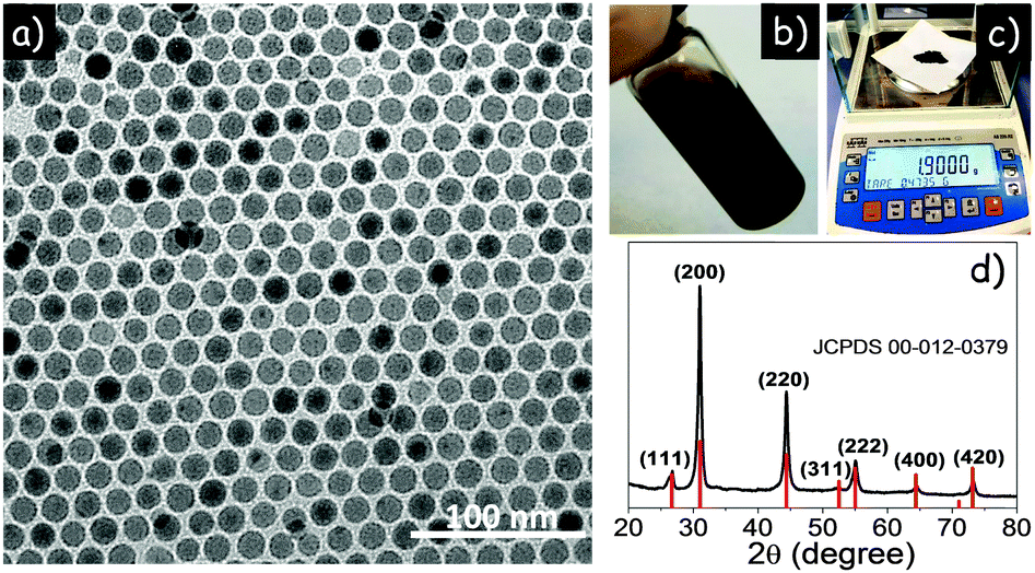 | ||
| Fig. 1 (a) TEM micrograph of the AgSbSe2 NCs. (b) NCs dispersed in chloroform. (c) The amount of NCs produced per batch. (d) The XRD pattern of AgSbSe2. | ||
The presence of OLA and OA in the precursor solution was required to dissolve AgNO3 and SbCl3, respectively.39 The absence of OA prevented the incorporation of Sb and thus the formation of stoichiometric AgSbSe2 NCs. Likewise, the absence of OLA resulted in a polydisperse mixture of AgSbSe2 and Ag2Se (Fig. S2 and S3, ESI†).
Although the reaction mixture already turned dark brown upon injection of the selenium precursor, relatively long reaction times were necessary to produce monodisperse NCs (Fig. 2 and Fig. S4, ESI†). Within the first 15 min, NCs with a bimodal size distribution were obtained. This bimodal distribution possibly originates from an extended nucleation time due to a relatively low reactivity of the precursor complexes, which translates into a slow NC growth that prevents a rapid monomer reduction in the supersaturation.40 A focusing of the size distribution, most probably mediated by an Ostwald ripening process, was observed up to 30 min of reaction time, when the narrowest size distribution was obtained. Larger reaction times resulted in a non-uniform growth of the NCs, increasing the size distribution width.
 | ||
| Fig. 2 (a–c) TEM micrographs of AgSbSe2 NCs prepared at a fixed temperature, 220 °C, and different reaction times: (a) 15 min; (b) 30 min; and (c) 60 min. (d) Histogram of the particle size distribution for NCs produced at increasing reaction times. (e and f) TEM micrographs of AgSbSe2 NCs prepared at different reaction temperatures and a fixed reaction time, 30 min: (e) 180 °C; (f) 200 °C; and (g) 240 °C (5 min). (h) Histogram of the measured particle size distribution for NCs produced at increasing reaction temperatures. | ||
Consistent with this growth mechanism, an increase of the injection and reaction temperature and thus of the monomer reactivity resulted in larger NCs. Therefore, fixing the reaction time, the AgSbSe2 NC size could be easily tailored in the range from 7 ± 1 nm to around 17 ± 2 nm by just adjusting the reaction temperature in the range from 180 to 240 °C (Fig. 2 and Fig. S5, ESI†). Reaction temperatures below 180 °C did not allow the growth of AgSbSe2 NCs. Higher reaction temperatures resulted in highly polydisperse NCs.
In the 1H nuclear magnetic resonance (NMR) spectrum of the resulting NC dispersion in deuteroform, slightly broadened resonances are observed which correspond to an oleyl chain (Fig. 3a). Since the integrations from the alkene resonance (5) and the CH3 resonance (6) fit the expected 2![[thin space (1/6-em)]](https://www.rsc.org/images/entities/char_2009.gif) :3 ratio we conclude that fully saturated molecules are not present. However, it is difficult to distinguish OA from OLA since the characteristic CH2 resonances (1 and 2) next to the functional group are not detected, presumably due to the interaction of the ligand with the NC surface. The nuclear Overhauser effect spectrum (NOESY) (Fig. 3b) indeed confirms that the oleyl species interact with the surface since negative (black) nOe cross peaks are observed.41 The total ligand concentration was determined to be 4.5 mM (based on resonance 6) and with the NC concentration and NC size, a rather low ligand density of 1.2 nm−2 was calculated. The diffusion ordered NMR spectrum (DOSY, Fig. 3c) features two sets of resonances (apart from acetone), with a different diffusion coefficient, D. This indicates that two species are present which diffuse with a different speed. However, none of the two species diffuses slow enough to correspond to a 15 nm nanocrystal plus a tightly bound ligand shell, which would yield a solvodynamic diameter, ds = 19 nm. We thus infer that the ligands are not tightly bound but are in a dynamic exchange regime between a free state and a bound state. Therefore, the ligand density that was calculated earlier is a maximum value and, in reality, the ligands only spend part of their time on the surface. A low bond strength of the ligands to the NC surface and the observed ligand dynamic exchange are consistent with the NC growth not being limited by the surfactant concentration, but by the growth kinetics.
:3 ratio we conclude that fully saturated molecules are not present. However, it is difficult to distinguish OA from OLA since the characteristic CH2 resonances (1 and 2) next to the functional group are not detected, presumably due to the interaction of the ligand with the NC surface. The nuclear Overhauser effect spectrum (NOESY) (Fig. 3b) indeed confirms that the oleyl species interact with the surface since negative (black) nOe cross peaks are observed.41 The total ligand concentration was determined to be 4.5 mM (based on resonance 6) and with the NC concentration and NC size, a rather low ligand density of 1.2 nm−2 was calculated. The diffusion ordered NMR spectrum (DOSY, Fig. 3c) features two sets of resonances (apart from acetone), with a different diffusion coefficient, D. This indicates that two species are present which diffuse with a different speed. However, none of the two species diffuses slow enough to correspond to a 15 nm nanocrystal plus a tightly bound ligand shell, which would yield a solvodynamic diameter, ds = 19 nm. We thus infer that the ligands are not tightly bound but are in a dynamic exchange regime between a free state and a bound state. Therefore, the ligand density that was calculated earlier is a maximum value and, in reality, the ligands only spend part of their time on the surface. A low bond strength of the ligands to the NC surface and the observed ligand dynamic exchange are consistent with the NC growth not being limited by the surfactant concentration, but by the growth kinetics.
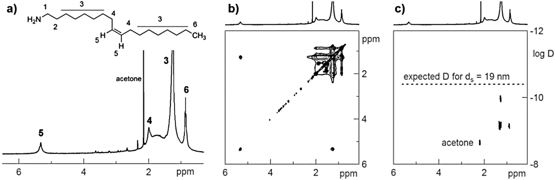 | ||
| Fig. 3 (a) 1H NMR spectrum of AgSbSe2 15 ± 2 nm NCs (4 μM) and the corresponding (b) NOESY and (c) DOSY spectra. | ||
To elucidate the nature of the two species in DOSY, we stripped the ligands from the NC surface by the addition of TFA. After removal of the NCs by centrifugation, the supernatant was again measured using NMR (Fig. S6, ESI†) and the characteristic resonances of both OA and OLA were observed with a relative abundance of 18% and 82% respectively.
Controlled amounts of bismuth were incorporated within the AgSbSe2 NCs by replacing a small amount of SbCl3 by an equivalent amount of Bi(CH3COO)3 in the precursor solution. At relatively low Bi concentrations, [Bi] < 5%, EDX analysis showed the final Bi composition in the NCs to match, within the experimental error, the nominal concentration of introduced Bi(CH3COO)3. The incorporation of Bi ions within the AgSbSe2 lattice was confirmed by a slight peak shift toward lower angles in the XRD pattern (Fig. 4b), pointing towards an increase of the lattice parameters. Bi-doping had also an evident influence on the size and shape distribution of the produced NCs (Fig. 4a).
 | ||
| Fig. 4 (a) TEM micrograph of AgSb0.98Bi0.02Se2 NCs and (b) their XRD pattern including the reference JCPDS 00-012-0379. The inset shows details of the (200) peak. | ||
To use AgSbSe2 NCs in solid-state devices that require an efficient transport of charge carriers, original insulating organic ligands have to be removed. Among the different ligand displacement agents tested, NaNH2 was the most effective one, as characterized by Fourier-transform infrared spectroscopy (FTIR). After ligand removal with a 0.02 M NaNH2 solution, AgSbSe2 could not be re-dispersed in non-polar solvents and the strong C–H vibration modes (2850–3000 cm−1) and the bands corresponding to C–C, C–N and NH2 (700–1650 cm−1) had completely disappeared from the FTIR spectrum (Fig. 5), proving the effective removal of OLA and OA from the NC surface.
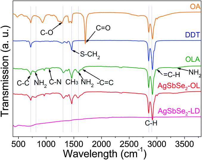 | ||
| Fig. 5 From top to down, FTIR spectra of pure OA, DDT, OLA, as-produced AgSbSe2 NCs (AgSbSe2-OL) and AgSbSe2 NC after ligand removal with NaNH2 (AgSbSe2-LD). | ||
After ligand displacement, dried 15 nm AgSbSe2 NCs were hot-pressed into 10 mm diameter and 1.5 mm thick pellets at 350 °C under 70 MPa pressure for 30 min. All pellets produced had a metallic lustre, were mechanically robust and had relative densities above 93% as measured by Archimedes' method. No secondary phases or changes in composition of the AgSbSe2 and AgSb0.98Bi0.02Se2 materials during the hot press process were detected by EDX and XRD (Fig. S7 and S8, ESI†). SEM and TEM characterization showed a very low porosity and large grains, up to several hundred nanometers, during the thermal processes (Fig. 6a and Fig. S9, ESI†). However, HRTEM characterization allowed discerning crystallographic order domains in the nanometer size regime (Fig. 6b).
 | ||
| Fig. 6 (a) SEM micrograph of the fractured surface of a AgSbSe2 pellet (inset); (b) HRTEM micrograph of the same AgSbSe2 pellet showing several crystal nanodomains. | ||
Fig. 7 shows the electrical conductivity (σ), Seebeck coefficient (S), thermal conductivity (κ), and thermoelectric figure of merit (ZT = σS2T/κ) of AgSbSe2 and AgSb0.98Bi0.02Se2 pellets. Both materials showed a p-type electronic character. AgSbSe2 was characterized by a relatively low σ, which increased from 1380 S m−1 at ambient temperature up to 1700 S m−1 at 600 K. It showed high Seebeck coefficients reaching up to 462 μV K−1 at 695 K, which relates with its flat valence band maximum and multipeak valence band structure.16 The introduction of an atomic 0.5% Bi significantly enhanced the electrical conductivity, which increased from 4520 S m−1 at room temperature to 5970 S m−1 at 618 K in AgSb0.98Bi0.02Se2. These values are slightly above those previously reported for bulk AgSb0.98Bi0.02Se2 produced by solid state methods.16 With Bi doping, the Seebeck coefficient decreased to values below 360 μV K−1, which is consistent with an increase of carrier concentration. Overall, the AgSb0.98Bi0.02Se2 power factor (PF) was higher than that of AgSbSe2, up to ∼0.74 mW m−1 K−2 at 580 K (Fig. S10, ESI†), and slightly higher than previously reported for bulk AgSb0.98Bi0.02Se2 (Fig. S12, ESI†).16
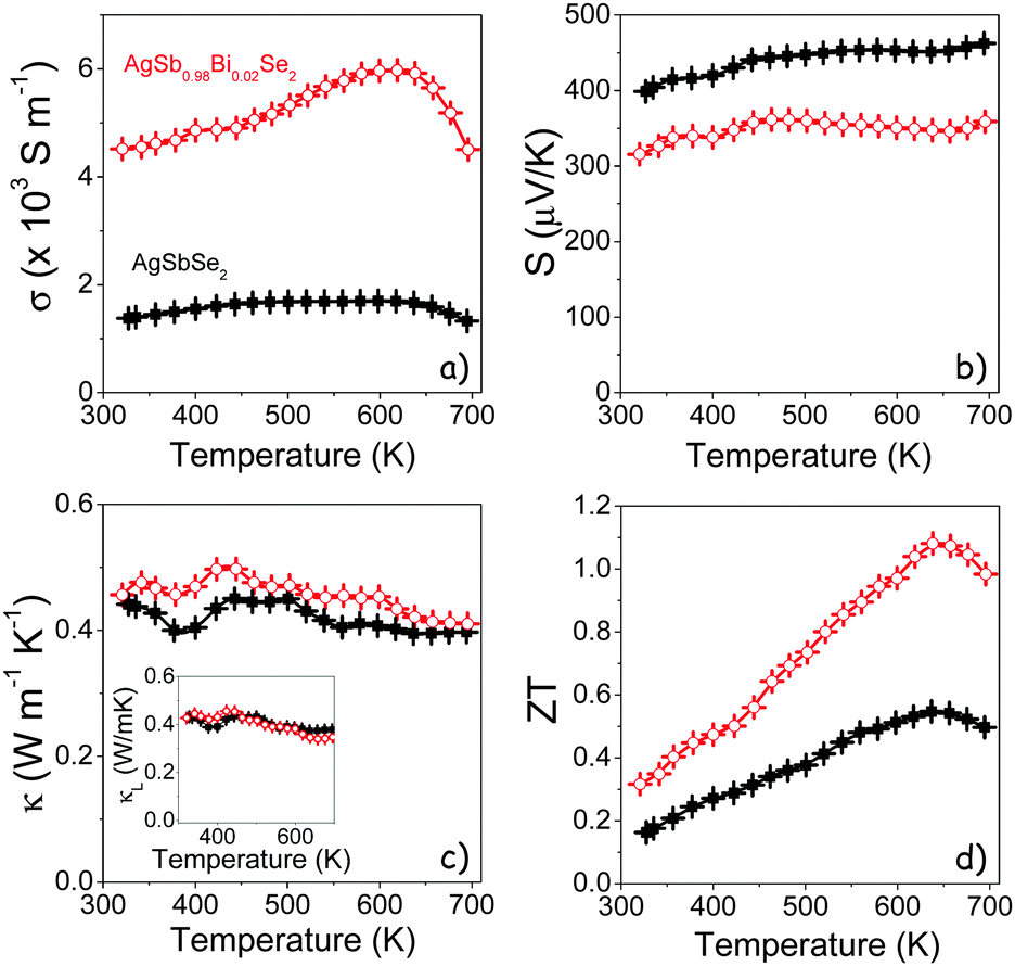 | ||
Fig. 7 Temperature dependence of: (a) electric conductivity (σ); (b) Seebeck coefficient (S); (c) thermal conductivity (κ) including lattice thermal conductivity (κL) in the inset; and (d) thermoelectric figure of merit (ZT) of AgSbSe2 (■) and AgSb0.98Bi0.02Se2 ( ). ). | ||
Room temperature Hall measurements provided hole concentrations p = 4 ± 2 × 1019 cm−3 in AgSbSe2 and 5-fold higher for AgSb0.98Bi0.02Se2, p = 2 ± 1 × 1020 cm−3. As in related Cu2SbSe342,43 and AgSbTe244–47 compounds, the origin of the p-type conductivity in AgSbSe2 is found in its defect structure and non-stoichiometry, and it is generally associated with Ag vacancies. The introduction of a small amount of an impurity may perturb the AgSbSe2 lattice and modify this defect concentration. In the particular case of substituting Sb3+ ions by the larger Bi3+ ions a compressive strain is introduced, which we hypothesize can in part be alleviated by a larger density of Ag vacancies and thus an increase of the hole concentration. The confirmation of this hypothesis needs in all cases a careful analysis of the defect formation energies within this compound in the presence of Bi, which is out of the scope of the present work. Besides, the relatively low Hall mobilities measured, 2.5 cm2 V−1 s−1 and 1.9 cm2 V−1 s−1 for AgSbSe2 and AgSb0.98Bi0.02Se2, respectively, are consistent with the large degree of disorder, the nanoscale precipitates and the intrinsically large effective mass of holes in this system. The mobility decrease with the introduction of Bi ions is also consistent with the presence of additional point defects scattering charge carriers.
Very low thermal conductivities (κtotal = λCpρ < 0.5 W m−1 K−1) were measured for both AgSbSe2 and AgSb0.98Bi0.02Se2 compounds in the whole studied temperature range of 300 to 700 K (Fig. 7c). These low thermal conductivities can be explained by an efficient multi-level phonon scattering; that is by nanometer scale precipitates, by the highly disordered lattice and by the strong phonon–phonon interactions from the high degree of anharmonicity of the Sb–Se bonds in this material.18 In spite of the higher density of defects associated with the presence of Bi, thermal conductivities were slightly higher for AgSb0.98Bi0.02Se2 due to the larger contribution from the electronic thermal conductivity (Fig. 7c inset).
As a result, ZT values of up to 1.1 at 640 K were obtained for AgSb0.98Bi0.02Se2 (Fig. 7d), which represents a two-fold increase over pristine AgSbSe2, and is among the best values obtained for a Pb- and Te-free material at this temperature (Table S1, ESI†).
4. Conclusions
In summary, a scalable colloidal synthesis of monodisperse AgSbSe2 NCs and Bi-doped AgSb1−xBixSe2 NCs was developed. We showed OLA and OA to be present in dynamic exchange at the surface of the NCs, rendering them soluble in non-polar solvents while allowing kinetic control of their growth. After displacing these surfactants, NCs were used as building blocks to produce 93% relative density nanomaterials. A preliminary optimization of the doping level resulted in AgSb0.98Bi0.02Se2 nanomaterials reaching ZT = 1.1 at 640 K. This figure of merit is among the largest values reported for a tellurium-free material in the middle temperature range, with the additional advantage of the low-cost and convenient solution processability of the materials and related devices.Acknowledgements
This work was supported by the European Regional Development Funds, the Framework 7 program under project UNION (FP7-NMP-2012-310250), the Swiss Federal Commission for Technology and Innovation (CTI, Project Nr. 14698.2 PFIW-IW) and the Spanish MINECO project BOOSTER (ENE2013-46624-C4-3-R). YL thanks the China Scholarship Council (CSC 201406500003) for scholarship support. MI, OD and SO thank AGAUR for their Beatriu de Pinós postdoctoral grant (2013 BP-A00344) and PhD grant, respectively. JDR thanks the FWO (Research Foundation Flanders) for financial support. M. V. K. acknowledges partial financial support from the European Union (EU) via FP7 ERC Starting Grant 2012 (Project NANOSOLID, GA No. 306733). The authors also acknowledge the funding from Generalitat de Catalunya 2014 SGR 1638.Notes and references
- K. Wang, C. Steimer, R. Detemple, D. Wamwangi and M. Wuttig, Appl. Phys. A: Mater. Sci. Process., 2005, 81, 1601–1605 CrossRef CAS.
- H. Soliman, D. Abdel-Hady and E. Ibrahim, J. Phys.: Condens. Matter, 1998, 10, 847 CrossRef CAS.
- K. Wang, C. Steimer and M. Wuttig, J. Optoelectron. Adv. Mater., 2007, 9, 2008 CAS.
- A. Patel and D. Lakshminarayana, Thin Solid Films, 1982, 98, 59–63 CrossRef CAS.
- A. Patel, D. Lakshminarayana and K. Rao, Thin Solid Films, 1982, 94, 51–57 CrossRef CAS.
- A. Abdelghany, S. Elsayed, D. Abdelwahab, A. A. El Ela and N. Mousa, Mater. Chem. Phys., 1996, 44, 277–280 CrossRef CAS.
- K. Wojciechowski and M. Schmidt, Phys. Rev. B: Condens. Matter Mater. Phys., 2009, 79, 184202 CrossRef.
- S. Geller and J. Wernick, Acta Crystallogr., 1959, 12, 46–54 CrossRef CAS.
- J. Wernick and K. Benson, J. Phys. Chem. Solids, 1957, 3, 157–159 CrossRef CAS.
- R. Wolfe, J. Wernick and S. Haszko, J. Appl. Phys., 1960, 31, 1959–1964 CrossRef CAS.
- L. Aggarwal, J. S. Sekhon, S. N. Guin, A. Arora, D. S. Negi, R. Datta, K. Biswas and G. Sheet, Appl. Phys. Lett., 2014, 105, 113903 CrossRef.
- E. Quarez, K.-F. Hsu, R. Pcionek, N. Frangis, E. Polychroniadis and M. G. Kanatzidis, J. Am. Chem. Soc., 2005, 127, 9177–9190 CrossRef CAS PubMed.
- K. Hoang, S. Mahanti, J. R. Salvador and M. G. Kanatzidis, Phys. Rev. Lett., 2007, 99, 156403 CrossRef PubMed.
- M. Salimi and S. J. Hashemifar, J. Alloys Compd., 2015, 650, 143–148 CrossRef CAS.
- K. Wojciechowski, J. Tobola, M. Schmidt and R. Zybala, J. Phys. Chem. Solids, 2008, 69, 2748–2755 CrossRef CAS.
- S. N. Guin, A. Chatterjee, D. S. Negi, R. Datta and K. Biswas, Energy Environ. Sci., 2013, 6, 2603–2608 CAS.
- J. Garza, S. Shaji, A. Rodriguez, T. D. Roy and B. Krishnan, Appl. Surf. Sci., 2011, 257, 10834–10838 CrossRef CAS.
- T. N. Asokan, K. Urmila, R. Jacob, R. R. Philip, G. Okram, V. Ganesan and B. Pradeep, J. Semicond., 2014, 35, 052001 CrossRef.
- J. González, S. Shaji, D. Avellaneda, A. Castillo, T. D. Roy and B. Krishnan, Mater. Res. Bull., 2013, 48, 1939–1945 CrossRef.
- K. Bindu, M. Nair, T. D. Roy and P. Nair, Electrochem. Solid-State Lett., 2006, 9, G195–G199 CrossRef CAS.
- K. Bindu, J. Campos, M. Nair, A. Sanchez and P. Nair, Semicond. Sci. Technol., 2005, 20, 496 CrossRef CAS.
- K. Wojciechowski, M. Schmidt, J. Tobola, M. Koza, A. Olech and R. Zybała, J. Electron. Mater., 2010, 39, 2053–2058 CrossRef CAS.
- S. N. Guin, D. S. Negi, R. Datta and K. Biswas, J. Mater. Chem. A, 2014, 2, 4324–4331 CAS.
- D. Li, X. Qin, T. Zou, J. Zhang, B. Ren, C. Song, Y. Liu, L. Wang, H. Xin and J. Li, J. Alloys Compd., 2015, 635, 87–91 CrossRef CAS.
- S. N. Guin and K. Biswas, J. Mater. Chem. C, 2015, 3, 10415–10421 RSC.
- S. N. Guin, A. Chatterjee and K. Biswas, RSC Adv., 2014, 4, 11811–11815 RSC.
- Z. Liu, J. Shuai, H. Geng, J. Mao, Y. Feng, X. Zhao, X. Meng, R. He, W. Cai and J. Sui, ACS Appl. Mater. Interfaces, 2015, 7, 23047–23055 CAS.
- S. Cai, Z. Liu, J. Sun, R. Li, W. Fei and J. Sui, Dalton Trans., 2015, 44, 1046–1051 RSC.
- E. M. Levin, S. L. Bud'ko and K. Schmidt-Rohr, Adv. Funct. Mater., 2012, 22, 2766–2774 CrossRef CAS.
- B. A. Cook, M. J. Kramer, J. L. Harringa, M. K. Han, D. Y. Chung and M. G. Kanatzidis, Adv. Funct. Mater., 2009, 19, 1254–1259 CrossRef CAS.
- D. V. Talapin, J.-S. Lee, M. V. Kovalenko and E. V. Shevchenko, Chem. Rev., 2009, 110, 389–458 CrossRef PubMed.
- M. V. Kovalenko, L. Manna, A. Cabot, Z. Hens, D. V. Talapin, C. R. Kagan, V. I. Klimov, A. L. Rogach, P. Reiss and D. J. Milliron, ACS Nano, 2015, 9, 1012–1057 CrossRef CAS PubMed.
- M. Ibáñez, R. Zamani, S. Gorsse, J. Fan, S. Ortega, D. Cadavid, J. R. Morante, J. Arbiol and A. Cabot, ACS Nano, 2013, 7, 2573–2586 CrossRef PubMed.
- M. Ibáñez, D. Cadavid, U. Anselmi-Tamburini, R. Zamani, S. Gorsse, W. Li, A. M. López, J. R. Morante, J. Arbiol and A. Cabot, J. Mater. Chem. A, 2013, 1, 1421–1426 Search PubMed.
- M. Ibáñez, R. J. Korkosz, Z. Luo, P. Riba, D. Cadavid, S. Ortega, A. Cabot and M. G. Kanatzidis, J. Am. Chem. Soc., 2015, 137, 4046–4049 CrossRef PubMed.
- D. Cadavid, M. Ibáñez, A. Shavel, O. J. Durá, M. L. de la Torre and A. Cabot, J. Mater. Chem. A, 2013, 1, 4864–4870 CAS.
- M. A. Connell, P. J. Bowyer, P. A. Bone, A. L. Davis, A. G. Swanson, M. Nilsson and G. A. Morris, J. Magn. Reson., 2009, 198, 121–131 CrossRef CAS PubMed.
- D. Sinnaeve, Concepts Magn. Reson., Part A, 2012, 40, 39–65 CrossRef.
- B. Zhou, M. Li, Y. Wu, C. Yang, W. H. Zhang and C. Li, Chem. – Eur. J., 2015, 21, 11143–11151 CrossRef CAS PubMed.
- J. Owen, Science, 2015, 347, 615–616 CrossRef CAS PubMed.
- Z. Hens and J. C. Martins, Chem. Mater., 2013, 25, 1211–1221 CrossRef CAS.
- X. Li, D. Li, H. Xin, J. Zhang, C. Song and X. Qin, J. Alloys Compd., 2013, 561, 105–108 CrossRef CAS.
- Y. Zhang, L. Xi, Y. Wang, J. Zhang, P. Zhang and W. Zhang, Comput. Mater. Sci., 2015, 108, 239–249 CrossRef CAS.
- L.-H. Ye, K. Hoang, A. Freeman, S. Mahanti, J. He, T. M. Tritt and M. Kanatzidis, Phys. Rev. B: Condens. Matter Mater. Phys., 2008, 77, 245203 CrossRef.
- B. Du, H. Li and X. Tang, J. Alloys Compd., 2011, 509, 2039–2043 CrossRef CAS.
- V. Jovovic and J. Heremans, Phys. Rev. B: Condens. Matter Mater. Phys., 2008, 77, 245204 CrossRef.
- R. Mohanraman, R. Sankar, F.-C. Chou, C.-H. Lee, Y. Iizuka, I. P. Muthuselvam and Y.-Y. Chen, APL Mater., 2014, 2, 096114 CrossRef.
Footnote |
| † Electronic supplementary information (ESI) available: Additional experimental details and TEM, XRD, EDX, and NMR data. See DOI: 10.1039/c6tc00893c |
| This journal is © The Royal Society of Chemistry 2016 |