
 Open Access Article
 This Open Access Article is licensed under a
 Creative Commons Attribution 3.0 Unported Licence
A new approach for additive-free room temperature sintering of conductive patterns using polymer-stabilized Sn nanoparticles†
Hiroaki
Shirai
,
Mai Thanh
Nguyen
,
Yohei
Ishida
and
Tetsu
Yonezawa
*
Division of Materials Science and Engineering, Faculty of Engineering, Hokkaido University, Kita 13, Nishi 8, Kita-ku, Sapporo, Hokkaido 060-8628, Japan. E-mail: tetsu@eng.hokudai.ac.jp; Fax: +81-11-706-7110
First published on 23rd February 2016
Abstract
Tin nanoparticles (Sn NPs) are of considerable interest for conductive printing because of their low melting temperature and low cost. In the present study, polyvinylpyrrolidone (PVP) stabilized metallic Sn NPs were synthesized by a polyol process and the size of Sn NPs was controlled from 15 to 89 nm by adjusting the amount of PVP. For the first time, we demonstrated that conductive patterns fabricated from the inks of metallic Sn NPs were achieved readily at room temperature under N2 without reducing gases or additives. The lowest obtained resistivity was 1.1 × 10⁻³ Ω cm, which was 100 times higher than that of bulk Sn. The size of Sn NPs, the amount of the stabilizing agent, and the low melting temperature of Sn NPs were found to be the main factors controlling the conductivity of the obtained Sn pattern in room temperature sintering. This study offers a new approach for the room temperature fabrication of conductive electronics using the printing technique.
1. Introduction
Metal nanoparticles (NPs) have been studied in recent years due to their unique size-dependent physical, chemical, and optical properties.1–3 One of these interesting size-dependent properties is melting point depression with a decrease in the size. In particular, the melting point of metal particles dramatically decreases when their size is reduced to the nanoscale; this has been demonstrated both theoretically and experimentally.4–7 The surface atoms of a crystal have lower coordination numbers than that of the bulk atoms, thus they bind more loosely to each other compared to the bulk atoms.6 Therefore a high ratio of the surface area to volume of NPs reduces their melting point significantly.8 On the basis of this phenomenon, controlling the size of NPs allows for the control of their melting point. As a result, metal NPs are of increasing interest for making inks in order to obtain conductive patterns at a low sintering temperature using the printing technique. In contrast to the conventional method called photolithography, conductive printing can produce a large-area pattern at a high speed by a simple process of just printing the ink, evaporating the solvent, and sintering.9–15 Conductive printing techniques do not require the deposition and removal of a mask, whereas the etching and disposal of useful materials to form the desired pattern are required in photolithography; therefore conductive printing is efficient, energy and cost effective, and environmentally friendly. For fabricating conductive patterns at low temperature using the printing technique, a conductive ink made of metallic NPs with good electrical conductivity, chemical stability, and low melting point is highly required.Until now, NPs of noble metals such as Au16,17 and Ag11–13,18,19 have been widely investigated for this purpose because of their high stability and conductivity. However, the high cost and sintering temperature of noble metal NPs limit their practical applications. In addition to the high energy consumption, a high sintering temperature causes a thermal stress which induces warpage of the substrate. Recently, sintering of Ag NPs at room temperature has been somehow achieved.20–22 However, in order to promote the aggregation and sintering of Ag NPs to obtain conductive patterns, addition of destabilizing agents and salts or exposure to HCl vapor is required during the sintering process. The existence of chlorine or salts in the conductive pattern can oxidize Ag, thus decreasing the stability of the conductive patterns in practical use. Some researchers have considered Cu as an alternative material to noble metals. Although Cu is cheaper than Au and Ag, sintering temperature of Cu9,10,23,24 NPs is still high and the oxidation of Cu often requires a reductive gas flow during the annealing process. Sometimes, decomposition of an organic Cu complex is required for sintering.25 Even though some other annealing methods have been suggested to substitute the conventional annealing procedure using ultrasound,26 laser,27,28 IR,29 plasma,30 and microwaves,31 these methods still consume high energy or often result in incomplete annealing.32,33
Therefore, conductive inks that are of low cost and that can be sintered at lower temperature without reductive gases or any additives are desirable. Researchers have paid considerable attention to Sn NPs as an alternative candidate. Because of the low melting point of the bulk Sn (i.e., 232 °C), the melting temperature of Sn NPs with size less than a few tens of nanometers is expected to be much lower;34 this melting point depression of Sn NPs can lead to the sintering of Sn NPs even near room temperature without the removal of the stabilizing agent. As a result, by using Sn NPs for low temperature sintering, not only the problems associated with materials and energy cost, thermal stress, warpage, and corrosive additives can be solved, but also flexible patterns on paper or plastic substrates can be fabricated using the printing technique.
Zou et al.35 used a chemical reduction method using NaBH4 for the synthesis of Sn NPs and successfully synthesized Sn NPs with different average diameters in the range of 30 to 80 nm. However, no clear melting point depression was observed due to the relatively large size and polydispersity of Sn NPs. Jo et al.36 synthesized fine Sn NPs with sizes ranging from 11 to 29 nm by a modified polyol process. They found that as the size of Sn NPs decreased, the melting point of Sn NPs became lower. Furthermore their study showed that the melting point of Sn NPs with an average diameter of 11 nm was 177.3 °C. Huang et al.37 reported the synthesis of Sn NPs with a size of 10.4 nm by mixing a Sn chloride precursor with a certain amount of PVP and excess NaBH4 in a reaction bath. But, the properties of the synthesized Sn NPs were not studied yet.
As described above, the synthesis of Sn NPs with the size of around 10 nm has been reported elsewhere, but there is still a lack of study on the sintering of Sn NPs at near room temperature. Jo et al.36 reduced the oxide layer on the surface of Sn NPs, then removed the residual polymer by plasma ashing and sintered Sn inks at 250 °C to obtain the Sn conductive film of 64.27 μΩ cm. Chee et al.34 synthesized Sn NPs with an average size of 8.0 nm, whose melting point was 128 °C. They used these Sn NPs as a binder for commercial Ag inks and obtained Ag–Sn conductive films after sintering at 170 °C. Sn NPs which have been reported still required sintering at more than 170 °C. The main reason for the high sintering temperature, despite the size of NPs being ten to several tens of nanometers, is owing to a thin oxide layer formed on the surfaces of Sn NPs in these previous studies. To realize the low sintering temperature and high conductivity of Sn patterns, it is important to prevent the formation of this oxide layer.34,36,37 Therefore, in the present study, Sn NPs stabilized by PVP were synthesized with reference to the modified polyol process that Jo et al. used,36 while all processes regarding the synthesis, purification, and fabrication of Sn NPs and Sn patterns were performed under an inert atmosphere (Ar or N2). The amount of input PVP was investigated as a key factor controlling both the particle size and surface oxidation of Sn NPs and the conductivity of the resulting Sn pattern. Furthermore, conductive inks of the as-synthesized Sn NPs were prepared, and then conductive patterns were successfully formed just after drying conductive inks at room temperature without any heat treatment and additives. The factors, including the size of NPs, the amount of protecting agent and the low melting point of small NPs, which influence the resistivity of the obtained Sn pattern will be discussed.
2. Experimental
2.1 Chemicals
Tin(II) acetate (Wako), polyvinylpyrrolidone (PVP K15, TCI), NaBH4 (Junsei), and 1,5-pentanediol (Junsei) were used as the precursor, protecting agent, reducing agent, and solvent for the synthesis of Sn NPs, respectively. Molecular sieves 3A 1/16 (Junsei) were used for the dehydration of 1,5-pentanediol. Other chemicals were used as received without further treatment.2.2 Synthesis of Sn NPs
In order to synthesize Sn NPs with various sizes, a certain amount of PVP was dissolved in 50 cm3 of 1,5-pentanediol in a 200 cm3 two-neck flask whose interior was cleaned with aqua regia. Then, the mixed solution was vacuumed for 3 hours to remove dissolved oxygen and water. After vacuuming, 0.3552 g of tin(II) acetate was introduced and stirred for 40 minutes under Ar. Then, the mixture was heated to 160 °C. Subsequently, 0.5675 g of NaBH4 which was dissolved in 10 cm3 of 1,5-pentanediol was injected into the reaction solution. The reaction solution changed from light yellow to black immediately after the injection of the reducing agent; this implies that the reduction of Sn ions took place smoothly. After 15 minutes, the resulting solution was cooled to room temperature. Then, 1-propanol was added to the NP dispersion and the dispersion was centrifuged for 30 min at 15![[thin space (1/6-em)]](https://www.rsc.org/images/entities/char_2009.gif) 000 rpm. The centrifuge tube was tightly capped. Addition of 1-propanol to Sn NPs before centrifugation and the removal of the supernatant after centrifugation were done in a nitrogen atmosphere to prevent oxidation. This purification process was repeated 3 times to purify Sn NPs. Different amounts of PVP were used to synthesize Sn NPs as follows, 5.3420, 2.6710, 0.8903, 0.1781, 0.0890, 0.0089, and 0.0018 g; this corresponds to the weight ratios between Sn and PVP (Sn:PVP (w/w)) of 1:30, 1:15, 1:5, 1:1, 1:0.5, 1:0.05, and 1:0.01, respectively. The reaction yield of Sn NPs was higher than 80% for all syntheses.
000 rpm. The centrifuge tube was tightly capped. Addition of 1-propanol to Sn NPs before centrifugation and the removal of the supernatant after centrifugation were done in a nitrogen atmosphere to prevent oxidation. This purification process was repeated 3 times to purify Sn NPs. Different amounts of PVP were used to synthesize Sn NPs as follows, 5.3420, 2.6710, 0.8903, 0.1781, 0.0890, 0.0089, and 0.0018 g; this corresponds to the weight ratios between Sn and PVP (Sn:PVP (w/w)) of 1:30, 1:15, 1:5, 1:1, 1:0.5, 1:0.05, and 1:0.01, respectively. The reaction yield of Sn NPs was higher than 80% for all syntheses.
2.3 Preparation of conductive inks and patterns of Sn NPs
The conductive inks of Sn NPs were prepared by re-dispersing the purified Sn NPs in 1-propanol. The weight concentration of the Sn NPs in all conductive inks was adjusted to 6 wt%. A 20 mm × 20 mm conductive pattern was fabricated by dropping the Sn conductive ink onto a glass substrate and then allowing it to naturally dry at room temperature. All procedures were done under a nitrogen atmosphere.2.4 Characterization and measurements
The crystal structure and phases of the obtained NPs were characterized using a Rigaku Miniflex II X-ray diffractometer (XRD, Cu Kα radiation, and at a scanning rate of 5° min−1). The morphology of Sn NPs was analyzed using a transmission electron microscope (TEM, JEOL JEM-2000FX, 200 kV). High resolution TEM images were collected using a scanning transmission electron microscope (STEM, FEI Titan3 G2 60–300, 300 kV). Samples for TEM and STEM analysis were prepared by dipping carbon-coated-copper grids in a dispersion of Sn NPs in 1-propanol. The XPS spectrum was measured using an X-ray photoelectron spectroscopic analyser (JPS-9200) in order to confirm the purity of Sn NPs. Sn NPs were deposited on Si wafer for XPS measurements. The amount of PVP remaining on the surface of the obtained Sn NPs was determined using a thermogravimetry analyzer (TGA, Shimadzu DTG-60H). TGA measurement was operated using air at a flow rate of 100 cm3 min−1 and at a heating rate of 5 °C min−1 from room temperature to 800 °C. The sheet resistance of the obtained Sn pattern was measured using a four-point probe equipment (Mitsubishi Chemical Corporation MCP-T610). The sheet resistance of a Sn pattern was calculated from the average of those measured from six different areas of the pattern. A field emission scanning electron microscope (FE-SEM, JEOL JSM-6701F, 15 kV) was used to observe the morphology and take the cross section images of the obtained Sn patterns. The resistivity of a Sn pattern was calculated from the measured sheet resistance and thickness of the pattern.3. Results and discussion
3.1 Crystal structure and morphology of the obtained Sn NPs using various amounts of PVP
Fig. 1 shows the XRD patterns of Sn NPs synthesized using various amounts of PVP. These XRD patterns exhibited only the peaks of metallic tin without any signals related to tin oxides; this is a good indication that anti-oxidative Sn NPs were successfully synthesized. Furthermore there is no boron signal detected in the XPS spectrum of Sn NPs synthesized using the lowest PVP amount, i.e. 0.0018 g, (Fig. S1, ESI†). This result indicated that highly pure Sn NPs were obtained. | ||
| Fig. 1 XRD patterns of Sn NPs synthesized using different amounts of PVP: (a) 5.3420, (b) 2.6710, (c) 0.8903, (d) 0.1781, (e) 0.0890, (f) 0.0089, and (g) 0.0018 g. The corresponding weight ratios of the input elemental Sn to PVP were indicated in the inset. The reference patterns of tetragonal SnO2 (JCPDS no. 41-1445) and Sn (JCPDS no. 04-0673) are also shown. | ||
The morphology of some of the representative Sn NPs synthesized using different amounts of PVP is shown in Fig. 2a–c (also see the TEM images of Sn NPs obtained under other conditions in the ESI,† Fig. S2). Sn NPs of average diameters of 15.2 ± 3.1 nm, 22.3 ± 5.1 nm, and 37.8 ± 12.5 nm were obtained using 5.3420, 0.0890, and 0.0089 g of PVP, respectively. The size of the obtained Sn NPs observed by TEM was similar to their crystallite size estimated from the line broadening of the XRD peaks using Scherrer's equation. Therefore, it can be concluded that the synthesized Sn NPs of 15 to 38 nm were single crystalline. For the case of the largest Sn NPs alone, the TEM size (89 nm) was different from the size calculated from Scherrer's equation (46 nm). This indicates that Sn NPs of more than 46 nm can be polycrystalline. Fig. 2d shows a HRTEM image for the near surface area of a Sn NP (25 nm) synthesized using 0.0890 g of PVP. The lattice fringes were observed clearly, and the measured lattice spacing of 0.29 nm corresponds to the (200) planes of β-Sn.38 This result suggested that highly pure metallic, single crystalline Sn NPs were synthesized, which also in good agreement with the XRD results where signals related to oxide phases were not observed. The fact that no surface oxide observed in Sn NPs is important, because tin oxides have much lower electrical conductivity and higher melting point, which prevent the sintering of NPs at low temperature with good conductivity. The change in the average diameter of the synthesized Sn NPs in relation to the amount of PVP used is shown in Fig. 2e. The size of Sn NPs decreased from 89 to 15 nm with the increase in the amount of PVP used. This was obtained since more PVP presented in the reaction solution prevented the further growth and aggregation of NPs more effectively, leading to the formation of Sn NPs of smaller size. These results suggested that PVP played a role of the protecting agent for Sn NPs and varying the PVP amount helped control the size of NPs over a wide range.
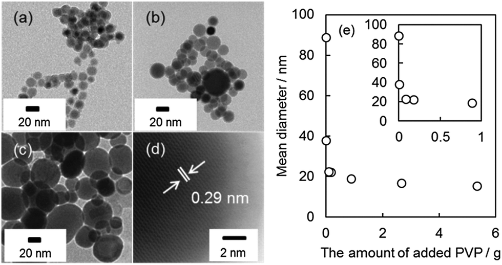 | ||
| Fig. 2 TEM images of Sn NPs synthesized using different amounts of PVP: (a) 5.3420, (b) 0.0890, and (c) 0.0089 g; (d) HRTEM image of a Sn NP (25 nm) obtained using PVP of 0.0890 g; (e) average diameter of Sn NPs synthesized with various amounts of PVP from 0.0018 to 5.3420 g. The inset shows the expansion plots of (e) from 0 to 1.0 g of the input PVP. | ||
3.2 The amount of PVP on the Sn NP surface
In order to study the relationship between the amounts of PVP left on the NP surface, the NP size, and the resistivity of the Sn pattern, it is necessary to estimate the PVP amounts for each size of Sn NPs from the thermogravimetric analysis. Fig. 3a shows the TGA results of Sn NPs synthesized using 0.1781 g of PVP. The weight increments were observed at about 220 °C (105.2 wt%) and 500 °C (120.9 wt%). Weight could be gained from the oxidation of Sn after heating Sn NPs in air. The amorphous oxides were reported upon exposure to air at low temperature.39 The partial oxidation of Sn to crystalline SnO (clearly detected at 400 °C) and complete oxidation to SnO2 (at 800 °C) during TGA measurement were confirmed as shown in the XRD patterns of the corresponding samples heated to 400 and 800 °C in air (Fig. S3, ESI†). This indicated that the formation of SnO and SnO2 contributed to the observed weight increases in the TGA result (Fig. 3a). Based on the fact that Sn NPs were completely oxidized to SnO2 after heating to 800 °C and PVP completely decomposed at around 600 °C in the air (Fig. S4, ESI†), the amount of PVP on the surface of Sn NPs was calculated from the weight increment in the TGA analysis. When Sn completely transforms to SnO2, it gives a theoretical weight increment of 127.0 wt%. The actual weight increment of 120.9 wt% was obtained from the TGA results (Fig. 3a) after SnO2 completely formed. The difference in the weight increments was attributed to the detachment of PVP remaining on the surface of Sn NPs. In this way, the amount of PVP was estimated for all samples synthesized using different PVP amounts (eqn (S1), ESI†).24Fig. 3b shows the relationship between the specific surface area of Sn NPs, which was calculated from the particle size and the input amount of precursor, and the amount of PVP on the surface of NPs. The amount of PVP is likely directly proportional to the specific surface area of NPs; this implies that the thickness of the PVP layer on the surface of Sn NPs was similar for each sample.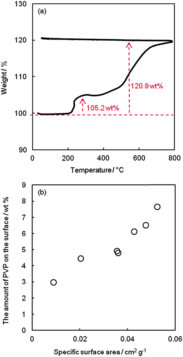 | ||
| Fig. 3 (a) A TGA curve of Sn NPs synthesized using 0.1781 g of PVP, and (b) the relationship between the specific surface area of Sn NPs and the PVP amount on the NP surface. | ||
3.3 Electrical conductivity of the room temperature sintered Sn films in relation to the PVP amount, NP size and morphology of the films
Sn conductive inks of 6 wt% Sn were successfully prepared by re-dispersing Sn NPs in 1-propanol (Fig. S5a, ESI†). These Sn conductive inks were dropped on the glass substrates and dried at room temperature, resulting in Sn conductive patterns with a surface area of 20 mm × 20 mm (Fig. S5b, ESI†), and a thickness of about 100 μm (Fig. S6, ESI†). The conductivity of Sn patterns was achieved by room temperature sintering for all samples. The obtained pattern with the lowest conductivity was also demonstrated to be sufficiently electron-conductive to turn on a LED tip (Fig. 4a).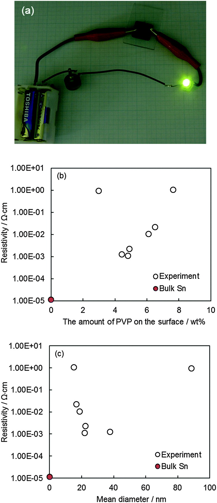 | ||
| Fig. 4 (a) An optical photograph of the conductive Sn pattern allowing the electrical conductive connection to light-up a LED tip. The resistivity of the Sn conductive patterns as a function of (b) the PVP amount on the surface of Sn NPs and (c) the NP size. A red point is for the resistivity of the bulk Sn. | ||
As PVP used to stabilize NPs is an organic polymer with low conductivity, the presence of the remaining PVP on the NP surface definitely has an important influence on the conductivity of the film made of Sn NPs. The resistivity of the Sn conductive patterns as a function of the amount of PVP on the surface of Sn NPs is shown in Fig. 4b. When larger amounts of PVP (7.6 wt%) are attached on the surface of Sn NPs, a high resistivity was obtained (1.0 × 100 Ω cm). As the amount of PVP on the surface of Sn NPs decreased from 7.6 to 4.4 wt%, the resistivity also decreased to the minimum value of 1.1 × 10⁻³ Ω cm (4.8 wt% PVP), and then remained almost constant at around 1.1 × 10⁻³ Ω cm (4.4–4.8 wt% PVP). In this regime of PVP amount (7.6−4.4 wt% PVP), a linear relationship between the resistivity of the pattern and the remaining PVP amount was observed. It was also found that the resistivity decreased with an increase in the size of Sn NPs (15 to 38 nm, Fig. 4c), of which the corresponding PVP amount on the particle surface decreased from 7.6 to 4.4 wt%. Since the amount of PVP remaining on the surface of NPs was reversely proportional to the size of the obtained Sn NPs, NPs of larger size have less PVP on its surface (Fig. S7, ESI†). The larger the NPs, the smaller the total surface area, and the lower the contact resistant and electron scattering. As a result, the greater conductivity is obtained. Therefore, the decrease in the PVP amount and the increase in the NP size both positively contributed to a good conductivity (decrease in the resistivity) of the pattern with the particle size ranging from 15.2 ± 3.1 to 37.8 ± 12.5 nm, and the surface PVP amount decreasing from 7.6 to 4.4 wt%.
When the PVP amount on the surface of NPs decreased from 4.4 to 3.0 wt%, the largest size of Sn NPs (i.e., 88.6 ± 21.3 nm, 3.0 wt% PVP) were obtained. These particles were also used to make the conductive pattern, but the resistivity sharply increased. This result indicated that in addition to the amount of PVP and the size of NPs, other factors also affected the resistivity of the conductive Sn pattern. Carefully investigating the morphology of the conductive pattern, we found that a significant fusion of Sn NPs occurred in the pattern prepared from Sn NPs of 37.8 ± 12.5 nm (Fig. 5a) while that was almost negligible in the pattern prepared from Sn NPs of 88.6 ± 21.3 nm (Fig. 5b). As a consequence, using Sn NPs of 37.8 ± 12.5 nm likely produced a more compact pattern and better sintering behavior than using Sn NPs of 88.6 ± 21.3 nm. In contrast, Fig. 5b shows almost no necking of the particles. The obtained results could originate from the melting of small Sn NPs observed in Sn NPs of 37.8 nm; these small Sn NPs helped larger NPs to join together and filled the space among the NPs in the pattern. The theoretical melting point of Sn versus the particle size calculated from the Gibbs–Thomson equation (eqn (S2))40 is shown in Fig. S8 ESI.† It is noticeable that Sn NPs of 10.5 nm could melt at 26 °C. Hence, these small Sn NPs can work as joint materials to improve the sintering. The melting of small Sn NPs also worked in other conductive patterns prepared using Sn NPs in the size range of 15 to 38 nm, but the effect of the melting of small Sn NPs on the decrease of the resistivity of the pattern as the NP size decreased was partly compensated by the high amount of PVP, surface area, and contact resistance owing to small NP sizes. Because of the lack of the small Sn NPs that melt and join other NPs in the pattern at room temperature, even though made from Sn NPs of the largest size (88.6 ± 21.3 nm) and least amount of PVP, the final Sn pattern still exhibited the highest resistivity. The lowest resistivity obtained for the pattern using Sn NPs of 22.0 ± 5.0 nm was achieved as the optimization of three factors including the NP size, the amount of PVP, and the amount of Sn NPs that can melt.
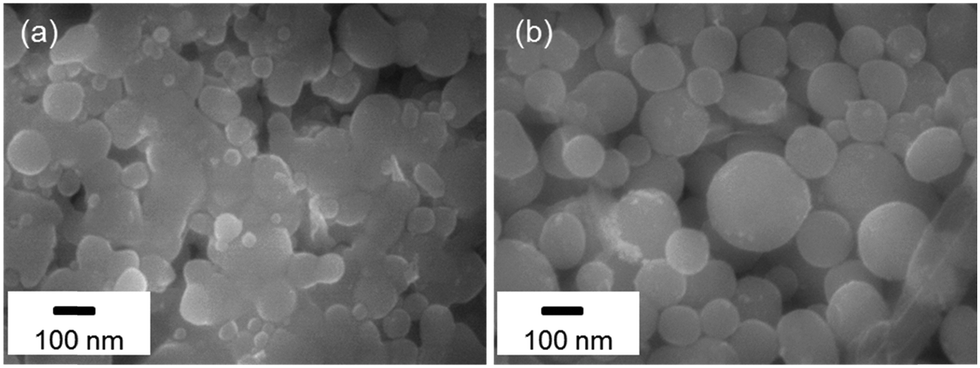 | ||
| Fig. 5 SEM images of the surface of Sn patterns made of Sn NPs synthesized using: (a) 0.0089 g PVP (Sn NPs of 37.8 ± 12.5 nm) and (b) 0.0018 g PVP (Sn NPs of 88.6 ± 21.3 nm). | ||
In order to demonstrate the room temperature binding effect of small Sn NPs, physical mixing of Sn NPs of largest size (88.6 ± 21.3 nm) and smallest size (15.2 ± 3.1 nm), both of which had the highest resistivity, was performed. The pattern fabricated from a mixture of Sn NPs (50 wt%) showed a lower resistivity than patterns made of either smallest or largest Sn NPs (Fig. 6). In this figure, the average resistivity of the patterns fabricated by only the smallest or the largest Sn NPs was used. It was known from above that the largest Sn NPs could not undergo necking with each other and the smallest NPs contained a large amount of PVP, resulting in high resistivities. The mixture gives a lower resistivity because smallest NPs play a role of glue, which makes connections among larger NPs. The resistivity decreased by the addition of the smallest Sn NPs to the largest Sn NPs, emphasizing the room temperature sintering effect of the smallest Sn NPs. In contrast, by mixing smallest Sn NPs with Sn NPs of 37.8 ± 12.5 nm (nearly lowest resistivity), no more decrease in the resistivity of the mixed-Sn NP pattern compared to that of the pattern fabricated from only Sn NPs of 37.8 ± 12.5 nm was detected (Fig. S9, ESI†). This suggests that the Sn NPs of 37.8 ± 12.5 nm contained an enough amount of small NPs to act as binders, and addition of the smallest Sn NPs did not reduce the conductivity. As shown in Fig. 4, the relationship between the PVP amount in Sn NPs and the resistivity of the patterns is linear in the range of the PVP amount in Sn NPs from 4.4 to 7.6 wt%. The ink made of Sn NPs in this range may have an enough amount of small Sn NPs, which could melt and act as binders. In other words, resistivity in this range depends only on the PVP amount and the size of Sn NPs.
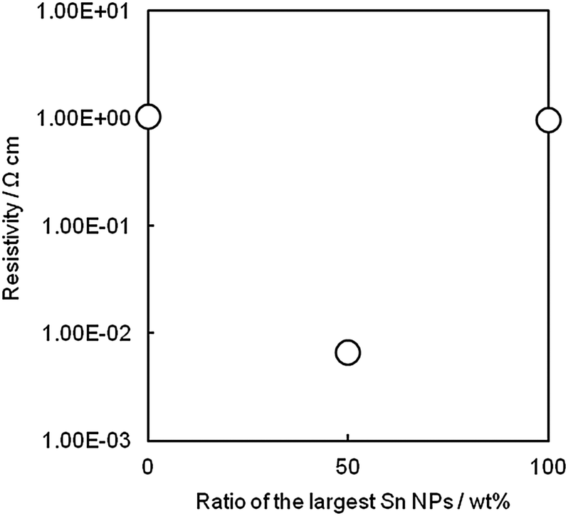 | ||
| Fig. 6 Resistivity of Sn patterns prepared from the smallest Sn NPs (15.2 ± 3.1 nm), the largest Sn NPs (88.6 ± 21.3 nm), and their mixture at 50 wt%. | ||
We also observed that in the case of Sn NPs with the average diameter of 37.8 nm (second largest Sn NPs) where their mixture with the smallest Sn NPs did not result in further decrease of resistivity, the minimum size of Sn NPs observed by TEM and the minimum size of Sn NPs in the sintered film at room temperature observed by SEM was 10 nm and 24 nm, respectively. Moreover, samples in which fusion of Sn NPs was observed contained at least 15% of Sn NPs with a size of less than 24 nm (Table S1, ESI†). On the other hand, Sn films without particle fusion did not show Sn NPs in this size range. These results indicated that in practical probably not only Sn NPs with the size smaller than 10 nm but also those with the size smaller than 24 nm can play a role of glue in room temperature sintering.
The sintering of Sn NPs at room temperature has been revealed for the first time and a low resistivity was achieved without any surface treatment, high temperature sintering, reducing gas or additives. Sn NPs with an average diameter of less than 10 nm was reported elsewhere,34 but they could not be used as a glue for room temperature sintering since there were an oxide layer hindering the NPs to join together. Other studies reported the use of Sn NPs for ink-jet printing at room temperature in the ambient atmosphere, but an plasma ashing with oxygen gas to remove the residual polymer and an additional high temperature H2 reduction step was required followed by high temperature (at more than 160 °C) sintering to obtain conductive Sn patterns.36 In our study, as metallic Sn NPs were synthesized and purified under an inert atmosphere, and inks and conductive patterns were prepared under N2, we could demonstrate the room temperature sintering of metallic Sn NPs without addition of corrosive additives and the achieved low resistivity of Sn patterns (1.1 × 10⁻³ Ω cm). The obtained resistivity is 100 times higher than that of bulk Sn and 17 times higher than that of Sn films fabricated by Jo et al.,36 who performed sintering at 250 °C for 1 h. This may be because of (i) avoiding the use of such high temperature sintering, (ii) PVP left on Sn NPs, and (iii) very diluted Sn loading in the ink. For further reduction of resistivity, using a decomposable polymer as a protective agent for Sn NPs or using more benign additives (short-chain amine compounds) will be considered. These studies are part of our future study.
4. Conclusions
PVP-stabilized metallic Sn NPs of various sizes were successfully synthesized in order to obtain low cost conductive inks and to achieve low temperature sintering. The size of Sn NPs was controlled in the range from 15 to 89 nm simply by changing the input amount of PVP. XRD showed no oxide peaks. Sn conductive inks were then prepared using the as-synthesized Sn NPs; and Sn conductive patterns with high conductivities were obtained readily at room temperature. The results of the present study illustrated three important factors that influence the resistivity of the conductive patterns: (i) the amount of PVP attached on the surface of Sn NPs, (ii) the number of contact points among Sn NPs (the size of Sn NPs), and (iii) the existence of Sn NPs which melt at room temperature. Without removing the protective polymer or introducing any additives, the lowest obtained resistivity of the Sn pattern was 1.1 × 10⁻³ Ω cm which was 100 times higher than that of bulk Sn and the highest achieved conductivity for the Sn pattern prepared from Sn NPs at room temperature. The existence of Sn NPs, which can act as binders and can undergo room temperature sintering, was revealed to be important for obtaining low resistivity in room temperature sintering in this study. We believe that the results presented in this study contribute low cost and highly conductive inks for room temperature sintering using the printing technique.Acknowledgements
This work was partially supported by KAKENHI (A, 24241041 to TY) from JSPS, Japan, and Murata foundation. Some characterization methods of tin nanoparticles were performed using the facilities of Nanotechnology platform, MEXT, Japan.Notes and references
- C.-P. Liang, Y. Yamauchi, C.-H. Liu and K. C.-W. Wu, Dalton Trans., 2013, 42, 8704 RSC.
- N. Toshima and T. Yonezawa, New J. Chem., 1988, 22, 1179 RSC.
- Y.-C. Yen, B. Creran and V. M. Rottello, Nanoscale, 2012, 4, 1871 RSC.
- P.-A. Buffat and J.-P. Borel, Phys. Rev. A: At., Mol., Opt. Phys., 1976, 13, 2287 CrossRef CAS.
- S. J. Zhao, S. Q. Wang, D. Y. Cheng and H. Q. Ye, J. Phys. Chem. B, 2001, 105, 12857 CrossRef CAS.
- F. G. Shi, J. Mater. Res., 1994, 9, 1307 CrossRef CAS.
- M. Schmidt, R. Kusche, B. V. Issendorff and H. Haberland, Nature, 1998, 393, 238 CrossRef CAS.
- H. Jiang, K.-S. Moon, F. Hua and C. P. Wong, Chem. Mater., 2007, 19, 4482 CrossRef CAS.
- M. Matsubara, T. Yonezawa, T. Minoshima, H. Tsukamoto, Y. Yong, Y. Ishida, M. T. Nguyen, H. Tanaka, K. Okamoto and T. Osaka, RSC Adv., 2015, 5, 102904 RSC.
- M. Matsubara, T. Yonezawa and H. Tsukamoto, Bull. Chem. Soc. Jpn., 2015, 88, 1755 CrossRef.
- J. Yeo, G. Kim, S. Hong, M. S. Kim, D. Kim, J. Lee, H. B. Lee, J. Kwon, Y. D. Suh, H. W. Kang, H. J. Sung, J.-H. Choi, W.-H. Hong, J. M. Ko, S.-H. Lee, S.-H. Choa and S. H. Ko, J. Power Sources, 2014, 246, 562 CrossRef CAS.
- J. Perelaer, M. Klokkenburg, C. E. Hendriks and U. S. Schubert, Adv. Mater., 2009, 21, 4830 CrossRef CAS PubMed.
- Y. M. Shin, H.-J. Kim, S. P. Jang and J.-H. Lee, J. Electron. Mater., 2014, 43, 3372 CrossRef CAS.
- E. Fisslthaler, S. Sax, U. Scherf, G. Mauthner, E. Moderegger, K. Landfester and E. J. W. List, Appl. Phys. Lett., 2008, 92, 183305 CrossRef.
- H. Sirringhaus, T. Kawase, R. H. Friend, T. Shimoda, M. Inbasekaran, W. Wu and E. P. Woo, Science, 2000, 290, 2123 CrossRef CAS PubMed.
- M. B. Cortie, M. J. Coutts, C. Ton-That, A. Dowd, V. J. Keast and A. M. McDonagh, J. Phys. Chem. C, 2013, 117, 11377 CAS.
- A. Gupta, S. Mandal, M. Katiyar and Y. N. Mohapatra, Thin Solid Films, 2012, 520, 5664 CrossRef CAS.
- Y. J. Moon, H. Kang, K. Kang, S.-J. Moon and J. Y. Hwang, J. Electron. Mater., 2015, 44, 1192 CrossRef CAS.
- Q. Huang, W. Shen, Q. Xu, R. Tan and W. Song, Mater. Chem. Phys., 2014, 147, 550 CrossRef CAS.
- S. Magdassi, M. Grouchko, O. Berezin and A. Kamyshny, ACS Nano, 2010, 4, 1943 CrossRef CAS PubMed.
- M. Grouchko, A. Kamyshny, C. F. Mihailescu, D. F. Anghel and S. Magdassi, ACS Nano, 2011, 5, 3354 CrossRef CAS PubMed.
- P. F. Moonen, E. Bat, W. P. Voorthuijzen and J. Huskens, RSC Adv., 2013, 3, 18498 RSC.
- Y. Yong, T. Yonezawa, M. Matsubara and H. Tsukamoto, J. Mater. Chem. C, 2015, 3, 5890 RSC.
- T. Yonezawa, H. Tsukamoto and M. Matsubara, RSC Adv., 2015, 5, 61290 RSC.
- T. Yonezawa, H. Tsukamoto, Y. Yong, M. T. Nguyen and M. Matsubara, RSC Adv., 2016, 6, 12048 RSC.
- H. Yamauchi, T. Dobashi and S. Sato, Chem. Lett., 2012, 41, 1154 CrossRef CAS.
- A. Watanabe, J. Photopolym. Sci. Technol., 2013, 26, 199 CrossRef CAS.
- G. Qin, A. Watanabe, H. Tsukamoto and T. Yonezawa, Jpn. J. Appl. Phys., 2014, 53, 096501 CrossRef.
- D. Tobjörk, H. Aarnio, P. Pulkkinen, R. Bollström, A. Määttänen, P. Ihalainen, T. Mäkelä, J. Peltonen, M. Toivakka, H. Tenhu and R. Österbacka, Thin Solid Films, 2012, 520, 2949 CrossRef.
- I. Reinhold, C. E. Hendriks, R. Eckardt, J. M. Kranenburg, J. Perelaer, R. R. Baumann and U. S. Schubert, J. Mater. Chem., 2009, 19, 3384 RSC.
- J. Perelaer, R. Jani, M. Grouchko, A. Kamyshny, S. Magdassi and U. S. Schubert, Adv. Mater., 2012, 24, 3993 CrossRef CAS PubMed.
- Y. H. Yoon, S.-M. Yi, J.-R. Yim, J.-H. Lee, G. Rozgonyi and Y.-C. Joo, Microelectron. Eng., 2010, 87, 2230 CrossRef CAS.
- T. Kumpulainen, J. Pekkanen, J. Valkama, J. Laakso, R. Tuokko and M. Mäntysalo, Opt. Laser Technol., 2011, 43, 570 CrossRef CAS.
- S.-S. Chee and J.-H. Lee, Thin Solid Films, 2014, 562, 211 CrossRef CAS.
- C.-D. Zou, Y.-L. Gao, B. Yang and Q.-J. Zhai, Trans. Nonferrous Met. Soc. China, 2010, 20, 248 CrossRef CAS.
- Y. H. Jo, I. Jung, C. S. Choi, I. Kim and H. M. Lee, Nanotechnology, 2011, 22, 225701 CrossRef PubMed.
- P.-C. Huang and J.-G. Duh, 2008 Electronic Components and Technology Conference (ECTC), 2008, 431.
- N. H. Chou and R. E. Schaak, J. Am. Chem. Soc., 2007, 129, 7339 CrossRef CAS PubMed.
- K. Kravchyk, L. Protesescu, M. I. Bodnarchuk, F. Krumeich, M. Yarema, M. Walter, C. Guntlin and M. V. Kovalenko, J. Am. Chem. Soc., 2013, 135, 4199 CrossRef CAS PubMed.
- T. Yonezawa, S. Arai, H. Takeuchi, T. Kamino and K. Kuroda, Chem. Phys. Lett., 2012, 537, 65 CrossRef CAS.
Footnote |
| † Electronic supplementary information (ESI) available: The XPS spectrum of Sn NPs; TEM images of Sn NPs synthesized using different amounts of PVP; XRD patterns of as-synthesized Sn NPs and after heating in air; the TG curve of only PVP; photographs of a Sn conductive ink and a conductive pattern; a SEM image of a conductive pattern; the relationship between the PVP amount on the surface of Sn NPs and the average diameter of Sn NPs; the calculation of the theoretical melting point of Sn NPs; resistivity of Sn patterns prepared from the Sn NPs of different sizes and their mixture; and the ratio of the number of Sn NPs with a diameter less than 24 nm. See DOI: 10.1039/c6tc00161k |
| This journal is © The Royal Society of Chemistry 2016 |