
 Open Access Article
 This Open Access Article is licensed under a
 Creative Commons Attribution 3.0 Unported Licence
Spontaneous generation of interlayers in OPVs with silver cathodes: enhancing Voc and lifetime†
B.
Shamieh
,
S.
Obuchovsky
and
G. L.
Frey
*
Department of Materials Science and Engineering, Technion – Israel Institute of Technology, Haifa 32000, Israel. E-mail: gitti@tx.technion.ac.il
First published on 28th January 2016
Abstract
A major contribution to the performance improvement of organic photovoltaic (OPV) devices is due to the successful engineering of the metal/organic interface by introducing interlayers. We suggest a new methodology for processing interlayers by the spontaneous segregation of additives to a silver cathode. The driving force for this special migration is the chemical interaction between the thiol end groups of the additive and the thermally deposited Ag metal atoms. In addition to the end groups, the additive is also selected to modify the Ag work function and effectively increase the device Voc. Here we show that a spontaneously generated hexa(ethyleneglycol)-dithiol (HEG-DT) interlayer at the P3HT:PCBM/Ag interface increases the Voc by over 0.1 V and enhances the device efficiency by more than 76%, to ∼3% PCE. The presence of the interlayer is confirmed by measuring the composition of the blend/Ag interface using XPS. Furthermore, the spontaneously generated interlayer also suppresses the oxidation of the organic/Ag interface and stalls the interfacial degradation. Consequently, due to the presence of the interlayer the life-time of non-encapsulated devices stored and operated under ambient conditions is increased by a factor of 7.
Introduction
The performance of OPV devices steadily increased in recent years, with the state-of-the-art devices now reaching over 11% efficiency.1 These improvements are mainly due to the availability of new materials, attaining control over the film nano-morphology and the successful engineering of the metal/organic interface. The latter requires adjustment of the chemical interactions and electronic band alignments at the metal/organic interface to support charge extraction. These strongly depend on the type of material used as the contact. The selection of the bottom electrode is limited by transparency and conductivity requirements, usually achieved by a doped metal oxide or conducting polymer film. The top contact, on the other hand, is generally a thermally evaporated metal film. The selection of the metal depends on the architecture of the device: either a direct architecture where electrons are collected by the top electrode or an inverted architecture where holes are collected by the top metal contact. Currently, the average performances of the direct architecture devices are significantly higher than those of the inverted structures.2 In the direct architecture, the top metal contact should attain a low work function for electron extraction, and hence, aluminum and calcium are the common preferences (Φ = 4.11 eV and 2.8 eV respectively).3,4 However, their low work function inherently imposes low environmental stability due to oxidation when exposed to ambient conditions5,6 and interaction with the underlying organic film.7 Indeed, the limited lifetime associated with direct architecture devices is often attributed to the oxidation of the metal electrode and not necessarily the degradation of the organic materials.8 Metals with higher stability, such as silver and gold, attain high work functions (Φ = 4.3 eV and 5.2 eV respectively),9 and are commonly used as anodes in OPVs. The integration of these metals as cathodes would impose a significant barrier for electron extraction.10Interlayers are often used to reduce barriers imposed by electrodes with unsuitable work functions.11 The interlayers can enhance charge collection by selectivity to one type of carrier,12,13 or by modifying the work function of the electrode. For example, it was demonstrated that interlayers composed of dipole-including molecules can tune the work function of an Al electrode effectively enhancing the device efficiency by 50%.14 Therefore, an ideal cathode design for OPVs would consist of a metal with a high intrinsic work function to provide stability against oxidation and a judiciously selected interlayer to lower the effective work function to allow electron collection.
Interlayers are generally deposited in discrete processing steps either before or after the deposition of the active layer. The main deposition techniques include thermal deposition in a high vacuum or spin coating using solvents orthogonal to the active layer.15,16 Recently, we have shown that interlayers can be spontaneously generated by inducing additive migration from the organic layer to the Al/organic interface during metal deposition.17 The driving force for interlayer formation is the interaction between the end group of the additive and the deposited metal clusters.18 This methodology allows the formation of functional interlayers, with no need for a discrete processing step, at the “buried” interface between the active layer and the top cathode.
In this study, we investigate the migration of an additive with thiol end groups towards the organic/Ag interface during Ag deposition. Silver was chosen as a cathode material since it provides a compromise between a relatively low work function metal for charge collection and reasonable environmental stability.19 Furthermore, unlike other metals, silver was also found to form an abrupt interface with the active layer that does not extend into the organic layer.8,20 To demonstrate the spontaneous interlayer formation at the blend/Ag interface we fabricated direct architecture bulk heterojunction (BHJ) devices of poly(3-hexylthiophene-2,5-diyl) (P3HT) and phenyl-C61-butyric acid (PCBM) blend with the HEG-DT additive (chemical structure shown in the inset of Fig. 1b). This additive consists of two thiol end groups and a C–O backbone which was recently shown to modify the work function of Al in OPVs.21 High Resolution Scanning Electron Microscopy (HRSEM), X-ray Photoelectron Spectroscopy (XPS), optical absorption measurements and J–V measurements under inert and ambient conditions confirm the spontaneous generation of a HEG-DT interlayer at the Ag/P3HT:PCBM interface and the corresponding work function modulation. Importantly, the presence of the additive interlayer at the active layer/cathode interface doubled the device efficiency and significantly enhanced the stability of non-encapsulated devices under ambient conditions.
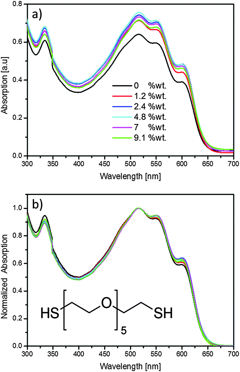 | ||
| Fig. 1 (a) As-measured, and (b) normalized optical absorption measurements of P3HT:PCBM:HEG-DT films with different concentrations of HEG-DT. The inset shows the chemical structure of HEG-DT. | ||
Experimental
Materials
P3HT (Sepiolid P100, regioregularity >95%) was purchased from Rieke Metals. PCBM was purchased from Nano-C. HEG-DT, Mw = 314.5 g mol−1 was purchased from Sigma Aldrich. All materials were used as received. Poly(3,4-ethylenedioxythiophene):polystyrene sulfonic acid (PEDOT:PSS) was acquired from Haraeus (Clevios PVP AL 4083) and was filtered through a 0.45 μm poly(tetrafluoroethylene) (PTFE) filter before use.Film deposition and device fabrication
Solar cell fabrication: ITO-covered glass was cleaned by sonication in acetone, methanol and isopropyl alcohol, followed by 15 minutes of a UV-ozone treatment to remove organic contaminations and to activate its surface for better PEDOT:PSS adhesion. PEDOT:PSS was spun at 5000 rpm and dried at 120 °C for 15 min under ambient conditions. The substrates were then transferred into a glovebox and kept under a nitrogen atmosphere throughout the device fabrication process.To a 1,2-dichlorobenzene solution of P3HT![[thin space (1/6-em)]](https://www.rsc.org/images/entities/char_2009.gif) :PCBM (20:20 mg ml−1) calculated amounts of HEG-DT were added to obtain solutions with 0, 1.2, 2.4, 4.8, 7, 9.1 and 13 wt% HEG-DT. The P3HT:PCBM:HEG-DT blend films were deposited by spin coating at 1500 rpm for 25 seconds onto the PEDOT:PSS/ITO substrates. The top silver layer was thermally deposited through a shadow mask at a system pressure of ∼7.5 × 10⁻⁶ Torr. The thickness of the Ag layer was 100 nm for the device cathodes directing a device area of 3 mm2, and the Ag thickness for the XPS measurements was ∼3 nm.
:PCBM (20:20 mg ml−1) calculated amounts of HEG-DT were added to obtain solutions with 0, 1.2, 2.4, 4.8, 7, 9.1 and 13 wt% HEG-DT. The P3HT:PCBM:HEG-DT blend films were deposited by spin coating at 1500 rpm for 25 seconds onto the PEDOT:PSS/ITO substrates. The top silver layer was thermally deposited through a shadow mask at a system pressure of ∼7.5 × 10⁻⁶ Torr. The thickness of the Ag layer was 100 nm for the device cathodes directing a device area of 3 mm2, and the Ag thickness for the XPS measurements was ∼3 nm.
Characterization
The absorption spectra were recorded using a Varian Cary 100 Scan 100 UV-vis spectrophotometer in the 300–700 nm range.High-resolution cross section images of cleaved samples were obtained using the Zeiss Ultra Plus high resolution scanning electron microscope (HRSEM), equipped with a Schottky field emission electron source. The images were acquired using both secondary electrons (SEs) and backscattered electrons (BSEs), at a relatively low accelerating voltage of 1 kV at a working distance of 2 mm.
X-ray Photoelectron Spectroscopy (XPS) was performed in a Thermo VG Scientific Sigma Probe fitted with a monochromatic Al Kα (1486.6 eV) source. A 100 W X-ray beam of 400 μm in diameter was used for high energy resolution scans of the C1s spectra with a pass energy of 30 eV. Line-shape analysis was done using the XPSPEAK 4.1 software after a Shirley-type background subtraction. The binding energy scale calibration of the C1s spectra was done by referencing the C–C/C–H binding signal to 285 eV. The same C1s energy shift correction was applied to correct the S2p spectra. For all samples, the C1s spectra were recorded in the standard and bulk-sensitive modes, i.e. with the angle between the direction of the analyzer and the specimen normal in the range 53° ± 3° or 30.5° ± 7.5°, respectively. Based on the inelastic mean free path estimation of the metal/blend system, the information depth of the C1s and S2p electrons is ∼5 nm thick organic film beneath the silver layer.22
Device characterization was performed in an inert atmosphere under a 100 mW cm−2 AM 1.5G class A sun simulator (science Tech Inc. ss150 solar simulator) using a Keithley 2400 source meter and a LabView automated data acquisition program recorded the J–V output. The ambient stability characterization was conducted following test ID: ISOS-D-1.23 However, to allow comparison with previous studies on similar device structures, the devices were not held at Voc while at rest.8,24,25 Between photovoltaic measurements, the devices were stored in the dark, at room temperature (∼25 °C) under ambient conditions (60% humidity). At least 16 devices of each type were measured and the reported values are the average values.
Results and discussion
To study the migration of additives from the BHJ to the blend/Ag interface during silver deposition, and the effect of the generated interlayer on OPVs we added calculated quantities of HEG-DT to solutions of P3HT:PCBM. HEG-DT was chosen as the additive because the C–O backbone was shown to modify the work function of Al cathodes, and because the affinity of the two thiol end groups to silver is expected to be the driving force for its migration towards silver clusters during evaporation.18 Importantly, the surface energy of HEG-DT was measured to be ∼55 mJ m−2 (see ESI†), which is higher than that of P3HT (∼27 mJ m−2) and PCBM (∼38 mJ m−2).26 Hence, the additive is not expected to enrich the air/blend surface during film deposition. By comparing the composition of the blend/air and blend/Ag interface we will be able to follow the migration of HEG-DT to the interface and correlate the interfacial composition with the device performance.Before focusing on the interlayer formation at the blend surface, it is necessary to confirm that the additive does not dramatically affect the bulk blend morphology. Therefore, we first studied the effect of adding HEG-DT on the P3HT:PCBM BHJ morphology by optical absorption. The absorption spectra of P3HT:PCBM:HEG-DT films with different concentration of HEG-DT in the film are presented in Fig. 1a. The spectra indicate that adding the selected quantities of HEG-DT to the blends only slightly increases film thickness (by less than ∼13%). Furthermore, all absorption spectra, regardless of HEG-DT content, still show the well-known absorption features of regioregular P3HT and PCBM. Namely, the two main vibronic transitions, at 520 and 560 nm, and shoulder at 605 nm of P3HT;27 and the main PCBM absorption signal at 335 nm.28 Notably, adding the HEG-DT to the blend induces changes only in the relative intensities of the different absorption peaks. To follow the relative intensities as a function of HEG-DT content we plot in Fig. 1b the normalized absorption spectra. The normalized data show that the addition of HEG-DT increases the intensity of the P3HT 605 nm shoulder with respect to the P3HT vibronic transitions and slightly decreases the intensity of the PCBM peak (335 nm). The 605 nm shoulder is associated with ordered P3HT domains and hence an increase in its intensity indicates that adding the additive improves the order in P3HT domains. In parallel, HEG-DT also slightly reduces the amount of PCBM in the film possibly due to the increased P3HT crystallinity which reduces the amount of PCBM in P3HT domains.29
After confirming that the HEG-DT does not significantly affect the bulk morphology, it is first necessary to confirm that the additive does not enrich the blend prior to metal deposition. The distribution and location of the additive in the as-spun blends are studied by comparing the cross section HRSEM images of an as-spun blend with no HEG-DT (Fig. 2a and b), to that with 43 wt% HEG-DT (Fig. 2c and d). This high HEG-DT concentration, significantly higher than that used for devices, is necessary for the imaging resolution. The SEM cross section image of the P3HT:PCBM blend (Fig. 2a) shows a homogenous film, while that of P3HT:PCBM:HEG-DT (43 wt%) (Fig. 2c) clearly shows a bilayer structure. Because HEG-DT is the component with the highest surface energy (see ESI,† Table S1), we hypothesize that above its solubility limit in the blend, it phase separates to the bottom of the film. The BSE micrographs, Fig. 2b and d, support this speculation. Fig. 2b shows a homogenous contrast indicating a similar electron density throughout the P3HT:PCBM film. However, the BSE micrograph of the P3HT:PCBM:HEG-DT (43 wt%) shows a bilayer structure consisting of a darker bottom and brighter top layer. The bright contrast is characteristic of high electron density, hence the top layer is associated with the semiconducting P3HT:PCBM blend. The bottom layer, therefore, consists of HEG-TD which has lower electron density hence a darker contrast. Importantly, we can conclude that before silver deposition, the HEG-DT location is governed by the thermodynamic consideration of surface energy, i.e. the excess HEG-DT (above solubility limit) enriches the film/bottom substrate interface.
 | ||
| Fig. 2 SE (a and c) and BSE (b and d) HRSEM cross-section images of P3HT:PCBM blends with no HEG-DT (a and b), and with 43 wt% HEG-DT (c and d). | ||
Now we turn to study the migration of the HEG-DT to the blend/Ag interface to generate the interlayer during the silver deposition. To do so, we spun the films onto PEDOT:PSS/ITO/glass substrates followed by thermal deposition of ∼3 nm-thick silver patches through a shadow mask (see schematic illustration in Fig. 3). The silver layer was thin enough for X-ray photoelectron spectroscopy (XPS) characterization of the underlying metal/organic interface. Note that the evaporation time was extremely short, less than 40 seconds and the sample temperature was kept under 25 °C, with no additional annealing processes. Under such conditions, all thermal effects are suppressed. Therefore, we can now use XPS to characterize the composition of the bare organic surface and adjacent organic/Ag interface of each film. Fig. 3 presents the bare-area (blue diamond) and silver-covered (red triangles) XPS spectra of films without (Fig. 3a) and with HEG-DT (Fig. 3b).
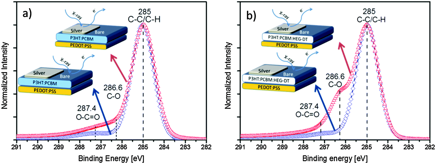 | ||
| Fig. 3 Normalized high energy resolution C1s XPS spectra of silver capped (red triangles) and bare (blue diamonds) areas of (a) P3HT:PCBM and (b) P3HT:PCBM:HEG-DT (4.8 wt%) blends. The insets show cross section illustrations of the respective areas characterized by XPS. | ||
All XPS spectra in Fig. 3, obtained from the bare organic surface or blend/Ag interface, with or without HEG-DT show a main C1s peak at 285 eV which is typical of C–C/C–H bonds. The XPS characteristic C–O signal of the HEG-DT C1s peak is expected at 286.6 eV.30 Indeed, the XPS spectra of films with no HEG-DT, Fig. 3a, show no peak at 286.6 eV. The weak signal at around 287.4 eV is associated with minor O–C![[double bond, length as m-dash]](https://www.rsc.org/images/entities/char_e001.gif) O contaminations upon exposure to ambient conditions. The HEG-DT finger-print signal is also absent from the XPS spectrum of the bare surface of the film with 4.8 wt% HEG-DT (Fig. 3b, blue diamonds), confirming that HEG-DT does not enrich the surface of the blend during spin coating. In contrast, the XPS spectrum of the same film (4.8 wt% HEG-DT) of the blend/Ag interface shows a clear C–O characteristic peak at 286.6 eV indicating that HEG-DT is present at the blend/Ag interface. Comparing the surface and bulk-sensitive XPS modes (see Experimental section and ESI,† Fig. S1) further confirms that the C–O peak at 286.6 eV originates from the buried blend/Ag interface and not the air/Ag interface. Thus, the XPS data presented in Fig. 3 unambiguously confirm the presence of the HEG-DT at the blend/Ag interface and not at the bare blend surface.
O contaminations upon exposure to ambient conditions. The HEG-DT finger-print signal is also absent from the XPS spectrum of the bare surface of the film with 4.8 wt% HEG-DT (Fig. 3b, blue diamonds), confirming that HEG-DT does not enrich the surface of the blend during spin coating. In contrast, the XPS spectrum of the same film (4.8 wt% HEG-DT) of the blend/Ag interface shows a clear C–O characteristic peak at 286.6 eV indicating that HEG-DT is present at the blend/Ag interface. Comparing the surface and bulk-sensitive XPS modes (see Experimental section and ESI,† Fig. S1) further confirms that the C–O peak at 286.6 eV originates from the buried blend/Ag interface and not the air/Ag interface. Thus, the XPS data presented in Fig. 3 unambiguously confirm the presence of the HEG-DT at the blend/Ag interface and not at the bare blend surface.
Following our previous studies,18 we speculate that the driving force for the HEG-DT migration to the blend/Ag interface is the strong affinity between the thiol end groups of HEG-DT and the silver clusters. This affinity is well known and seminal in the field of self-assembled monolayers (SAMs).31,32 To identify the thiol–Ag interaction at the blend/Ag interface we conducted XPS also at the S2p region. The XPS spectra of the silver-covered and bare areas of P3HT:PCBM and P3HT:PCBM:HEG-DT (4.8 wt%) films are presented in Fig. 4. The spectrum of the bare P3HT:PCBM blend surface (Fig. 4a) shows a doublet at 164 eV associated with the P3HT sulfur signal with the spin–orbit splitting expected ratio of 1:2.33 The S2p XPS spectrum of the bare surface of P3HT:PCBM:HEG-DT (4.8 wt%) (Fig. 4c) is generally identical to that of the P3HT:PCBM surface (Fig. 4a), confirming the absence of new sulfur moieties at the interface and indicating that HEG-DT did not segregate to the bare surface. A weak broad peak is generally seen at 168 eV (magenta squares) and is ascribed to sulfonate SOx contaminations.34
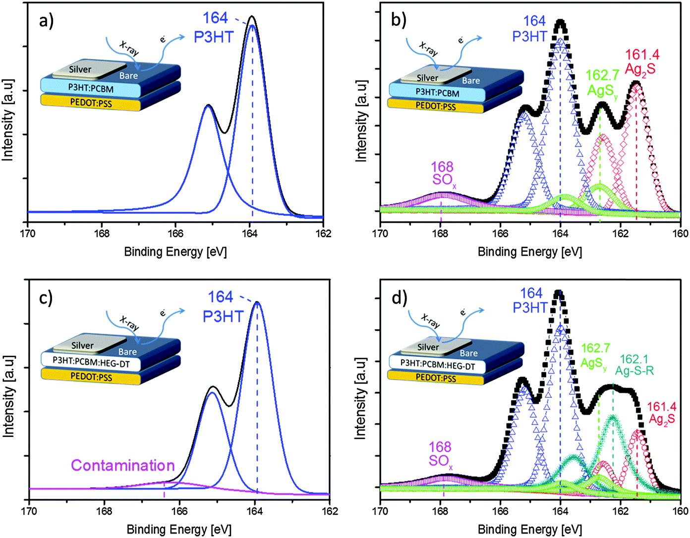 | ||
| Fig. 4 High energy resolution S2p XPS spectra deconvolution of (a) bare P3HT:PCBM, (b) silver capped P3HT:PCBM. (c) Bare P3HT:PCBM:HEG-DT (4.8 wt%), (d) silver capped P3HT:PCBM:HEG-DT (4.8 wt%) blends. The insets show cross section illustrations of the respective areas characterized by XPS. | ||
In contrast to the spectra of the bare organic surfaces, the S2p XPS spectra of the blend/Ag interfaces show new signals due to interaction between the organic components and the deposited silver. The Ag/P3HT:PCBM XPS spectrum, Fig. 4b, now includes new and strong signals in addition to the doublet at 164 eV and the weak and wide SOx contamination peak. The lower energy doublet, at 161.4 eV (red diamonds), can be assigned to silver sulfide (Ag2S) moieties originating from the P3HT–Ag interaction.33 The second doublet at 162.7 eV (green circles) is also associated with P3HT–Ag interactions forming Ag–S species labelled as AgSy.33 The presence of the HEG-DT in the blend dramatically modifies the S2p XPS spectrum of the blend/Ag interface. The XPS spectrum of the Ag/P3HT:PCBM:HEG-DT film (Fig. 4d) presents a new doublet peak (dark cyan stars) at 162.1 eV which could be associated with new thiolate species Ag–S–R35 due to interactions between HEG-DT and silver, on the expense of some thiophene–Ag interactions. Similar interactions have been previously identified for a dithiol monolayer on Au at 162.0 eV.34 Importantly, the spectra does not include the free thiol (R–SH) peak, at ∼163.5–164 eV,34 further supporting the formation of a chemical interaction between the HEG-DT end groups and the depositing silver clusters.
The combined C1s (Fig. 3) and S2p (Fig. 4) XPS spectra confirm the absence of HEG-DT at the blend/air interface and its presence at the blend/Ag interface. We suggest that during blend spin coating, the high surface energy of HEG-DT suppresses its enrichment of the blend/air interface. Consequently, the additive is homogeneously suspended in the film, up to its solubility limit, including near the surface. Its concentration at the blend/air interface is extremely low, under the XPS detection limit. During the metal deposition, the molecules residing close to the surface interact with the silver clusters imposing a HEG-DT concentration gradient. This gradient of HEG-DT near the surface induces the further migration of HEG-DT molecules from the film's bulk to the blend/Ag interface until the driving force for the migration is terminated. The HEG-DT interlayer at the blend/Ag interface is sufficient to modify the silver's work function. A similar migration mechanism has been previously reported for Al and a PEG additive.17,36
After confirming the presence of a HEG-DT interlayer at the blend/Ag interface, we can now utilize this interlayer for reducing the energy barrier at the cathode of a corresponding OPV device. A shift of the silver cathode's work function due to the interlayer will be translated to an increase in the device's Voc.37,38 A series of direct structure OPVs composed of P3HT:PCBM blends with different HEG-DT concentrations, capped by a silver cathode, were prepared and measured. Based on previous studies on a similar system,39 the devices were deliberately not further thermally annealed in order to demonstrate the spontaneous segregation of the additive towards the silver electrode during its deposition. The average J–V curves and performance details are presented in Fig. 5 and Table 1, respectively. Representative curves in the dark are shown in the ESI,† Fig. S2. The results clearly show that introducing HEG-DT to the P3HT:PCBM blends does not significantly affect the photocurrent but rather increases the Voc by >0.1 eV, regardless of the HEG-DT concentration. The FF, on the other hand, and hence also the device efficiency steadily increase with HEG-DT concentration. While the average efficiency of a device with no HEG-DT is 1.2%, that of a device with HEG-DT is more than double. The highest power conversion efficiency (PCE) achieved was 2.9% which is one of the highest reported values for direct structure P3HT:PCBM devices with Ag cathodes.
 | ||
| Fig. 5 Average current density–voltage (J–V) curves under illumination of glass/ITO/PEDOT:PSS/P3HT:PCBM:HEG-DT/Ag OPV devices with various content of HEG-DT. | ||
| wt% HEG-DT | V oc [V] | J sc [mA cm−2] | FF | PCE [%] |
|---|---|---|---|---|
| 0 | 0.44 ± 0.02 | 6.93 ± 0.55 | 0.45 ± 0.03 | 1.42 ± 0.17 |
| 1.2 | 0.55 ± 0.01 | 7.46 ± 0.26 | 0.49 ± 0.01 | 1.99 ± 0.08 |
| 2.4 | 0.56 ± 0.01 | 7.77 ± 0.84 | 0.51 ± 0.01 | 2.22 ± 0.11 |
| 4.8 | 0.56 ± 0.01 | 7.92 ± 0.76 | 0.53 ± 0.01 | 2.35 ± 0.28 |
| 7 | 0.56 ± 0.01 | 7.86 ± 0.20 | 0.55 ± 0.01 | 2.42 ± 0.06 |
| 9.1 | 0.57 ± 0.01 | 7.9 ± 0.68 | 0.56 ± 0.01 | 2.51 ± 0.01 |
| 13 | 0.56 ± 0.01 | 7.8 ± 0.44 | 0.59 ± 0.01 | 2.50 ± 0.16 |
The increase in Voc and the corresponding increase in device performance confirm the XPS measurements which identified the presence of a HEG-DT interlayer at the blend/Ag interface. Furthermore, these results are in good agreement with our recent studies showing that the presence of a PEG interlayer at the Al/P3HT:PCBM interface leads to a 33% increase in Voc and doubled the device efficiency.21 We speculate here too that the spatial proximity of the dipole-containing ethylene glycol moiety of HEG-DT to the silver electrode effectively reduces its work function, leading to the higher Voc, as schematically shown in Fig. 6. It is important to mention that oxidation of silver at the blend/Ag interface could not be the source of this Voc increase because the formation of Ag–O bonds is known to increase the work function of silver,40 and hence would decrease the Voc of the device.
 | ||
| Fig. 6 A schematic illustation of the enegy level allignment in the studied photovoltaic devices with and without the HEG-DT interlayer. | ||
Finally, because silver is reasonably environmentally stable,41 the non-encapsulated devices were kept in the dark under ambient conditions and their performance measured as a function of storage time. Under such conditions, we follow the degradation of the blend/Ag interface when exposed to oxygen and water, which is generally reported as the primary cause of device's degradation.19,25 The degradation of PCE of non-encapsulated devices with and without HEG-DT stored under ambient conditions and recorded over 7 days (10000 minutes) is shown in Fig. 7 (for the initial performance parameters and the decay curves of the other PV parameters, see ESI,† Fig. S3a–c). The devices were exposed to light for 5 minutes during each measurement, resulting in a total light exposure of approximately 120 minutes over the 7 days.
 | ||
| Fig. 7 Normalized PCE of non-encapsulated devices without HEG-DT (black circles) and with HEG-DT (red squares), stored under ambient conditions and recorded over 7 days (10000 minutes). | ||
Fig. 7 reveals that devices with HEG-DT show not only better performance but also significantly higher stability compared to devices with no HEG-DT. Namely, adding HEG-DT enhances the device lifetime, i.e. the degradation time to 50% of the initial efficiency, is extended by a factor of ∼7 (from 60 minutes to 450 minutes). In conventional P3HT:PCBM devices, the fast decay in efficiency is attributed to a fast roll-off in FF and Voc while the Jsc is generally maintained.42,43 In OPVs with silver electrodes the degradation is usually associated with interfacial degradation44 of either the blend/Ag interface or the blend/PEDOT:PSS interface. In the direct structure OPVs, the degradation is dominated by the blend/Ag interface because the blend/PEDOT:PSS interfaces are buried at the bottom of the device.8 The source of the blend/Ag interface degradation is the diffusion of moisture and air, resulting in an oxidation of the interface. This oxidation causes a steady increase in the silver work function, which in turn increases the barrier for electron extraction and favours hole extraction.25
To compare the degradation of OPV devices with and without HEG-DT we listed in Table 2 the percentage of photovoltaic parameter degradation after 100 minutes of exposure to air. First, we examine the degradation behaviour of the devices with no HEG-DT. Table 2 and time dependent J–V measurements (see ESI,† Fig. S3–S5) reveal that the Jsc of the devices with no HEG-DT decays more moderately than the Voc and the FF. This behaviour was shown to originate from a work function increase of silver due to oxygen and moisture diffusion from the sides of the silver electrodes and creation of Ag-oxide moieties at the blend/Ag interface. The same trend is observed in the devices with HEG-DT, however, the decay rate is much slower. The improved stability of the HEG-DT included devices is attributed to the presence of HEG-DT at the interface, which stalls the oxidation rate. Namely, introducing the HEG-DT to P3HT:PCBM leads to spontaneous generation of an interlayer at the blend/Ag interface which has two significant contributions: (i) it reduces the Ag work function which enhances the Voc effectively doubling the device performance; and (ii) passivates the Ag buried surface inhibiting its oxidation and dramatically enhancing the ambient stability.
| Photovoltaic parameter | P3HT:PCBM [% degradation] | P3HT:PCBM:HEG-DT (4.8 wt%) [% degradation] |
|---|---|---|
| J sc | 20 | 8 |
| V oc | 35 | 13 |
| FF | 78 | 22 |
| PCE | 61 | 25 |
Conclusions
In summary, in this study we used the conventional P3HT:PCBM blend in a direct architecture as a research platform to study the segregation of an additive, HEG-DT, to the blend/Ag interface and its effect on the device Voc and ambient stability. We showed that HEG-DT migrates to the blend/Ag interface during Ag deposition without affecting the BHJ morphology. The driving force for the migration is the high affinity of the end-group thiols for silver. During silver deposition, HEG-DT molecules close to the blend surface interact with depositing silver clusters forming a metal–organic complex, as identified by XPS. This interaction generates a HEG-DT concentration gradient in the film leading to further migration of the additive to the blend/Ag interface. The migration terminates when a HEG-DT interlayer is formed. Importantly, the HEG-DT interlayer reduces the silver work function and hence increases the device Voc, effectively doubling the device's efficiency. Moreover, it was demonstrated that the HEG-DT interlayer also enhances the life-time of un-encapsulated devices stored under ambient conditions by a factor of 7, by stalling the silver oxidation at the blend/Ag interface. Therefore, we demonstrated that spontaneous processes in organic and polymer matrices can be judiciously harnessed to direct and control the metal/organic interface in OPVs. This approach could also be expanded to other organic electronic devices such as organic field effect transistors and organic light emitting diodes and to encapsulations and coating technologies.Acknowledgements
This research was supported by a grant from GIF, the German-Israeli Foundation for Scientific Research and Development.References
- M. A. Green, K. Emery, Y. Hishikawa, W. Warta and E. D. Dunlop, Prog. Photovoltaics, 2015, 23, 1–9 Search PubMed.
- H.-H. Hsieh, Y.-M. Sung, F.-C. Hsu, K.-J. Hsiao, Y.-J. Lee and Y.-F. Chen, RSC Adv., 2015, 5, 1549–1556 RSC.
- D. L. Matz, E. L. Ratcliff, J. Meyer, A. Kahn and J. E. Pemberton, ACS Appl. Mater. Interfaces, 2013, 5, 6001–6008 CAS.
- E. D. Gomez and Y.-L. Loo, J. Mater. Chem., 2010, 20, 6604–6611 RSC.
- P. Dannetun, M. Boman, S. Stafström, W. R. Salaneck, R. Lazzaroni, C. Fredriksson, J. L. Brédas, R. Zamboni and C. Taliani, J. Chem. Phys., 1993, 99, 664–672 CrossRef CAS.
- J. Tang, X. Wang, L. Brzozowski, D. A. R. Barkhouse, R. Debnath, L. Levina and E. H. Sargent, Adv. Mater., 2010, 22, 1398–1402 CrossRef CAS PubMed.
- Z. Chunfu, Y. Hao, T. Shi-Wun, L. Zhenhua, F. Qian, E.-T. Kang and C. Zhu, IEEE Trans. Electron Devices, 2011, 58, 835–842 CrossRef.
- M. T. Lloyd, D. C. Olson, P. Lu, E. Fang, D. L. Moore, M. S. White, M. O. Reese, D. S. Ginley and J. W. P. Hsu, J. Mater. Chem., 2009, 19, 7638–7642 RSC.
- H. B. Michaelson, J. Appl. Phys., 1977, 48, 4729–4733 CrossRef CAS.
- H. R. Yeom, J. Heo, G.-H. Kim, S.-J. Ko, S. Song, Y. Jo, D. S. Kim, B. Walker and J. Y. Kim, Phys. Chem. Chem. Phys., 2015, 17, 2152–2159 RSC.
- T. M. Khan, Y. Zhou, A. Dindar, J. W. Shim, C. Fuentes-Hernandez and B. Kippelen, ACS Appl. Mater. Interfaces, 2014, 6, 6202–6207 CAS.
- E. L. Ratcliff, B. Zacher and N. R. Armstrong, J. Phys. Chem. Lett., 2011, 2, 1337–1350 CrossRef CAS PubMed.
- B. Qi, Z.-G. Zhang and J. Wang, Sci. Rep., 2015, 5, 7803 CrossRef CAS PubMed.
- Y. Zhou, C. Fuentes-Hernandez, J. Shim, J. Meyer, A. J. Giordano, H. Li, P. Winget, T. Papadopoulos, H. Cheun, J. Kim, M. Fenoll, A. Dindar, W. Haske, E. Najafabadi, T. M. Khan, H. Sojoudi, S. Barlow, S. Graham, J.-L. Brédas, S. R. Marder, A. Kahn and B. Kippelen, Science, 2012, 336, 327–332 CrossRef CAS PubMed.
- Y. Wei, P.-J. Liu, R.-H. Lee and C.-P. Chen, RSC Adv., 2015, 5, 7897–7904 RSC.
- J. Kesters, T. Ghoos, H. Penxten, J. Drijkoningen, T. Vangerven, D. M. Lyons, B. Verreet, T. Aernouts, L. Lutsen, D. Vanderzande, J. Manca and W. Maes, Adv. Energy Mater., 2013, 3, 1180–1185 CrossRef CAS.
- I. Deckman, M. Moshonov, S. Obuchovsky, R. Brener and G. L. Frey, J. Mater. Chem. A, 2014, 2, 16746–16754 CAS.
- I. Deckman, S. Obuchovsky, M. Moshonov and G. L. Frey, Langmuir, 2015, 31, 6721–6728 CrossRef CAS PubMed.
- M. Jørgensen, K. Norrman and F. C. Krebs, Sol. Energy Mater. Sol. Cells, 2008, 92, 686–714 CrossRef.
- J. Wang, C. R. Friedman, W. Cabrera, K. Tan, Y.-J. Lee, Y. J. Chabal and J. W. P. Hsu, J. Mater. Chem. A, 2014, 2, 15288–15293 CAS.
- I. Dekman, R. Brener and G. L. Frey, J. Mater. Chem. C, 2013, 1, 6522–6525 RSC.
- S. Tanurna, Surf. Interface Anal., 1991, 17, 927–939 CrossRef.
- M. O. Reese, S. A. Gevorgyan, M. Jørgensen, E. Bundgaard, S. R. Kurtz, D. S. Ginley, D. C. Olson, M. T. Lloyd, P. Morvillo, E. A. Katz, A. Elschner, O. Haillant, T. R. Currier, V. Shrotriya, M. Hermenau, M. Riede, K. R. Kirov, G. Trimmel, T. Rath, O. Inganäs, F. Zhang, M. Andersson, K. Tvingstedt, M. Lira-Cantu, D. Laird, C. McGuiness, S. Gowrisanker, M. Pannone, M. Xiao, J. Hauch, R. Steim, D. M. DeLongchamp, R. Rösch, H. Hoppe, N. Espinosa, A. Urbina, G. Yaman-Uzunoglu, J.-B. Bonekamp, A. J. J. M. van Breemen, C. Girotto, E. Voroshazi and F. C. Krebs, Sol. Energy Mater. Sol. Cells, 2011, 95, 1253–1267 CrossRef CAS.
- M. O. Reese, M. S. White, G. Rumbles, D. S. Ginley and S. E. Shaheen, Appl. Phys. Lett., 2008, 92, 053307 CrossRef.
- J. B. Kim, C. S. Kim, Y. S. Kim and Y.-L. Loo, Appl. Phys. Lett., 2009, 95, 183301 CrossRef.
- D. M. DeLongchamp, R. J. Kline and A. Herzing, Energy Environ. Sci., 2012, 5, 5980–5993 CAS.
- T.-A. Chen, X. Wu and R. D. Rieke, J. Am. Chem. Soc., 1995, 117, 233–244 CrossRef CAS.
- S. Cook, H. Ohkita, Y. Kim, J. J. Benson-Smith, D. D. C. Bradley and J. R. Durrant, Chem. Phys. Lett., 2007, 445, 276–280 CrossRef CAS.
- S. Obuchovsky, B. Shamieh, I. Deckman, G. Ankonina and G. L. Frey, Sol. Energy Mater. Sol. Cells, 2015, 143, 280–283 CrossRef CAS.
- G. Beamson and D. Briggs, High Resolution XPS of Organic Polymers, John Wiley & Sons, New York, 1992 Search PubMed.
- W. Lewandowski, M. Fruhnert, J. Mieczkowski, C. Rockstuhl and E. Górecka, Nat. Commun., 2015, 6, 6590 CrossRef PubMed.
- P. E. Laibinis, G. M. Whitesides, D. L. Allara, Y. T. Tao, A. N. Parikh and R. G. Nuzzo, J. Am. Chem. Soc., 1991, 113, 7152–7167 CrossRef CAS.
- L. Scudiero, H. Wei and H. Eilers, ACS Appl. Mater. Interfaces, 2009, 1, 2721–2728 CAS.
- W. Khalid, M. El Helou, T. Murböck, Z. Yue, J.-M. Montenegro, K. Schubert, G. Göbel, F. Lisdat, G. Witte and W. J. Parak, ACS Nano, 2011, 5, 9870–9876 CrossRef CAS PubMed.
- M. Zharnikov, J. Electron Spectrosc. Relat. Phenom., 2010, 178–179, 380–393 CrossRef CAS.
- X. Li, Y. Hu, Z. Deng, L. Zhu, Y. Wang, D. Xu, Y. Hou and F. Teng, Phys. Status Solidi A, 2015, 212, 1800–1804 CrossRef CAS.
- J. C. Nolasco, G. Ramos-Ortiz, J. L. Maldonado, O. Barbosa-Garcia, B. Ecker and E. von Hauff, Appl. Phys. Lett., 2014, 104, 043308 CrossRef.
- C. J. Brabec, A. Cravino, D. Meissner, N. S. Sariciftci, T. Fromherz, M. T. Rispens, L. Sanchez and J. C. Hummelen, Adv. Funct. Mater., 2001, 11, 374–380 CrossRef CAS.
- J. Vinokur, I. Deckman, S. Obuchovsky, K. Weinfeld and G. Frey, Proc. SPIE, Organic Photovoltaics XVI, vol. 9567, 2015, p. 95670X.
- W. C. Ho, Y. K. Soo, K.-B. Kim, Y.-H. Tak and J.-L. Lee, Appl. Phys. Lett., 2005, 86, 012104 CrossRef.
- C. S. Kim, J. B. Kim, S. S. Lee, Y. S. Kim and Y.-L. Loo, Org. Electron., 2009, 10, 1483–1488 CrossRef CAS.
- A. Puetz, T. Stubhan, M. Reinhard, O. Loesch, E. Hammarberg, S. Wolf, C. Feldmann, H. Kalt, A. Colsmann and U. Lemmer, Sol. Energy Mater. Sol. Cells, 2011, 95, 579–585 CrossRef CAS.
- M. T. Lloyd, C. H. Peters, A. Garcia, I. V. Kauvar, J. J. Berry, M. O. Reese, M. D. McGehee, D. S. Ginley and D. C. Olson, Sol. Energy Mater. Sol. Cells, 2011, 95, 1382–1388 CrossRef CAS.
- M. O. Reese, M. S. White, G. Rumbles, D. S. Ginley and S. E. Shaheen, Appl. Phys. Lett., 2008, 92, 053307 CrossRef.
Footnote |
| † Electronic supplementary information (ESI) available. See DOI: 10.1039/c5tc04141d |
| This journal is © The Royal Society of Chemistry 2016 |