
 Open Access Article
 This Open Access Article is licensed under a Creative Commons Attribution-Non Commercial 3.0 Unported Licence
Electrochemically deposited nanocrystalline InSb thin films and their electrical properties
K. E.
Hnida
*a,
S.
Bäßler
b,
J.
Mech
c,
K.
Szaciłowski
a,
R. P.
Socha
d,
M.
Gajewska
a,
K.
Nielsch
be,
M.
Przybylski
af and
G. D.
Sulka
g
aAGH University of Science and Technology, Academic Centre for Materials and Nanotechnology, al. A. Mickiewicza 30, 30-059 Krakow, Poland. E-mail: khnida@agh.edu.pl; katarzyna.hnida@gmail.com; Tel: +48 12 617 52 82
bUniversity of Hamburg, Multifunctional Nanostructures, Institute of Nanostructure and Solid State Physics, Jungiusstrasse 11, 20-355 Hamburg, Germany
cAGH University of Science and Technology, Faculty of Non-Ferrous Metals, Al. A. Mickiewicza 30, 30-059 Krakow, Poland
dJerzy Haber Institute of Catalysis and Surface Chemistry Polish Academy of Sciences, Niezapominajek 8, 30-239 Krakow, Poland
eLeibniz Institute for Solid State and Materials Research Dresden, PO Box 270116, 01171 Dresden, Germany
fAGH University of Science and Technology, Faculty of Physics and Applied Computer Science, al. A. Mickiewicza 30, 30-059 Krakow, Poland
gJagiellonian University in Krakow, Department of Physical Chemistry and Electrochemistry, Ingardena 3, 30-060 Krakow, Poland
First published on 13th January 2016
Abstract
We present an electrochemical route to prepare nanocrystalline InSb thin films that can be transferred to an industrial scale. The morphology, composition, and crystallinity of the prepared uniform and compact thin films with a surface area of around 1 cm2 were investigated. The essential electrical characteristics such as conductivity, Seebeck coefficient, the type, concentration and mobility of charge carriers have been examined and compared with InSb nanowires obtained in the same system for electrochemical deposition (fixed pulse sequence, temperature, electrolyte composition, and system geometry). Moreover, obtained thin films show much higher band gap energy (0.53 eV) compared to the bulk material (0.17 eV) and InSb nanowires (0.195 eV).
A Introduction
From a practical point of view, materials for modern electronic devices must fulfill certain basic requirements such as high material quality, scalability, good electrical performance, reproducibility and inexpensive synthesis procedure. III–V semiconductor thin films due to their incredible electrical properties are widely applicable in novel opto- and nanoelectronic devices. Among the binary compounds of III–V groups, the p- and n-type semiconducting indium antimonide (InSb) with a small band gap is a promising material, bulky n-InSb has a very high electron mobility of ∼80000 cm2 V−1 s−1 due to the presence of anion vacancies. When the charge carriers are holes, p-type conductivity with a carrier mobility of about 1250 cm2 V−1 s−1 is observed. Because of its good transport properties, InSb is used in gas sensors,1 biological sensors,2 magnetoresistors,3 IR detectors4 having a spectral response range from 3 to 5 μm and thermoelectric generators.5 Due to the plenitude and diversity of these applications, it is necessary to precisely control the microstructure and electrical properties of this material. The synthesis of indium antimonide thin films with a defined chemical composition and crystallinity is a difficult task. Currently, the most commonly used techniques are thermal evaporation,6 solid-source molecular beam epitaxy,7 electron beam evaporation,8 radio frequency sputtering9 and metalorganic chemical vapor deposition (MOCVD).10,11 Among others, electrodeposition is a relatively low cost and easy to use method that allows to synthesize binary and ternary compounds with different compositions. Therefore, it is often used for the synthesis of galvanic coatings and various kinds of nanowires such as metallic,12 semiconductor,13 polymeric14 and hybrid.15 In particular, the use of the pulse sequence during deposition allows not only to obtain a material with a uniform crystal size, but by changing the pulse duration it is also possible to synthesize films of varying grain sizes, which consequently affect the electrical properties. The properties of thin films strongly depend on their chemical composition. In addition, the effect of widening of the energy band gap in thin films can be achieved in two ways: by preparation of the film containing of a few atomic layers or by synthesizing a material composed of nanocrystals. Furthermore, widening of the band gap may result for the increasing carrier concentration via doping. Therefore, the preparation of semiconductors with a widened band gap opens up new possibilities for the practical application of such materials, for example in detectors covering a wide infrared spectral range.In this paper, we present the straightforward and applicable on an industrial scale electrochemical deposition of nanocrystalline InSb thin films showing widened band gap in comparison with the previously reported layers and bulk material. The characterization of the film morphology, composition, crystallinity and electric properties at room temperature was conducted. The proposed method of synthesis and characterization of the electrical properties of electrodeposited InSb thin films has not been reported so far.
B Experimental
The InSb films were electrodeposited from the aqueous plating bath containing InCl3·3H2O, SbCl3·3H2O, citric acid and sodium citrate from Alfa Aesar. The ingredients of analytical grade purity were used as received.The electrodeposition of indium and antimony was performed using 1.5 × 1.5 cm electropolished (H3PO4 + ethanol, 5![[thin space (1/6-em)]](https://www.rsc.org/images/entities/char_2009.gif) :2 in volume, 80 mA cm−2) and chemically etched (0.5 M H2SO4) Cu substrates. Before electrodeposition, an Au layer (20 nm) was sputtered on Cu. All electrodepositions were performed at room temperature in a conventional three-electrode cell (100 cm3 in volume) with a platinum counter electrode and an Ag/AgCl electrode as a reference electrode. The potentiostatic pulse electrodeposition of binary thin films was carried out from a citrate bath (0.2 M citric acid, 0.15 M sodium citrate) containing 0.06 M In3+ and 0.045 M Sb3+. Using a Reference 3000 potentiostat (Gamry Instruments), the InSb synthesis was performed at 20 °C at Eon = −2.3 V and Eoff = −0.5 V vs. Ag/AgCl. The pulse duration and delay time were 1 ms and 5 ms, respectively.
:2 in volume, 80 mA cm−2) and chemically etched (0.5 M H2SO4) Cu substrates. Before electrodeposition, an Au layer (20 nm) was sputtered on Cu. All electrodepositions were performed at room temperature in a conventional three-electrode cell (100 cm3 in volume) with a platinum counter electrode and an Ag/AgCl electrode as a reference electrode. The potentiostatic pulse electrodeposition of binary thin films was carried out from a citrate bath (0.2 M citric acid, 0.15 M sodium citrate) containing 0.06 M In3+ and 0.045 M Sb3+. Using a Reference 3000 potentiostat (Gamry Instruments), the InSb synthesis was performed at 20 °C at Eon = −2.3 V and Eoff = −0.5 V vs. Ag/AgCl. The pulse duration and delay time were 1 ms and 5 ms, respectively.
To achieve a compact structure of thin films, during codeposition of In3+ and Sb3+ ions, a pulse electrodeposition technique with a pulse sequence shown in the inset of Fig. 1A was used. During the Eon pulse (ton = 1 ms) the reduction processes described elsewhere occurred.16 At the ‘off’ time (toff = 5 ms), there was almost no electrodeposition observed. What is more, a partial dissolution of the top film layer, which could have a non-stoichiometric composition, occurred. A potential value of the off pulse is slightly different from the open circuit potential (OCP) of the system, however using a fixed pulse sequence allows to achieve reproducible nanocrystalline layers with a stoichiometric composition (tested over 20 samples). The dependence between deposition time and film thickness is shown in Fig. 1A. A growth rate of films obtained by pulse deposition was ca. 29 nm min−1. The average thickness of InSb films which were used to determine electrical properties was 1.5 μm.
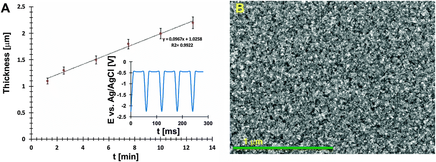 | ||
| Fig. 1 Relation between the thickness of the obtained InSb film and electrodeposition time (A) together with pulse electrodeposition sequence (inset) and SEM image (B) of the InSb layer with 1.5 μm thickness. | ||
The structural and morphological characterization studies of binary thin films were performed using a field-emission scanning electron microscope (FE-SEM/EDS, Hitachi S-4700 with a Noran System 7). The crystallinity of the obtained InSb films was examined using a Rigaku Mini FlexII diffractometer. For the analysis of diffraction patterns, the ICDD (International Centre for Diffraction Data) database, PDF Card No. 01-089-3667, was used. A thin InSb foil for transmission electron microscopy imaging was cut from a thin film using focus ion beam (FIB) FEI Quanta 3D 200i. Transmission electron microscopy (TEM) investigations were carried out using a FEI Tecnai TF20 X-TWIN (FEG) microscope equipped with an EDAX system, at an accelerating voltage of 200 kV. The film thickness and the crystal diameter were measured by using a profilometer (DektakXT Bruker). The atomic composition and electronic states of the elements were analyzed by X-ray photoelectron spectroscopy (XPS). The XPS spectrometer was equipped with a hemispherical analyzer SES R4000 (Gammadata Scienta) and an Al Kα X-ray source (1486.6 eV). The maximum energy resolution of the spectrometer for the line Ag 3d5/2 was 1.0 eV (for an analyzer pass energy of 100 eV). The electron binding energy (BE) scale was calibrated at the Fermi edge. The curves were fitted with Voigt profiles (GL = 30) and a Shirley background using Casa XPS software 2.3.12. The reflectance spectra of prepared thin films were recorded using a FTIR THERMO/Nicolet 5700 spectrophotometer, excitonic peak was fitted with GRAMS 32 software.
Sheet resistivity measurements of prepared thin films (with defined geometry) were performed at least ten times on each sample using a non-contact sheet resistance tester (EDDyCus® TF lab 2020, Suragus Sensors & Instruments). The Seebeck coefficient of the prepared samples was measured using a Potential-Seebeck Microprobe (PSM). Cross plane temperature gradient (ΔT) was applied and thermovoltage U (U = −SΔT, where S – Seebeck coefficient) was measured. The Seebeck coefficient was measured with an uncertainty of <3%.
C Results and discussion
A SEM image of the electrochemically deposited InSb thin film with a uniform grain size is shown in Fig. 1B.The XRD analyses allow a non-destructive study of the compositional variation of InSb thin films (Fig. 2A). To prevent surface oxidation of stoichiometric InSb, a 30 nm carbon layer was sputtered. The three reflections at 23.5, 39.4 and 46.7° (inset in Fig. 2A) are typical for indium antimonide ((111), (220) and (311)) and correspond to the regular structure of zinc blend. However, the intensity of peaks corresponding to the InSb phase is low. For this reason, additional selected area electron diffraction (SEAD) analysis was carried out. Fig. 2B shows the bright field TEM image with a marked area where the SAED analysis (inset) was performed. Fig. 2C shows a representative high resolution TEM image confirming the polycrystalline nature of the obtained thin film. The estimated crystallite size (d) was within the range of 20–30 nm.
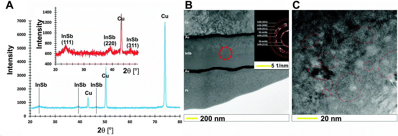 | ||
| Fig. 2 XRD diffraction pattern (A) and bright field TEM-SAED analysis (B) together with (C) high resolution TEM image for as-prepared InSb thin films with stoichiometric composition. | ||
For practical applications of nanocrystalline films, it is crucial for the material to contain a stoichiometric amount of appropriate atoms suitable for forming the desired compound but not an alloy. The surface states of the prepared InSb thin film were analyzed by XPS (Fig. 3). A typical In 3d core level spectrum (Fig. 3A) exhibits the In–Sb bonds identified at BE of 444.3 eV and 451.9 eV. These data are in agreement with the previously reported binding energies of In 3d doublet components at 444.2 and 451.8 eV for the bulk InSb.17 In InSb thin films we observe a slight shift (0.1 eV) towards higher energies. No other electronic states of indium are found by XPS. The Sb 3d and O 1s peaks are overlapped, however can be deconvoluted into two O 1s components and two doublet Sb 3d ones. The maximum of Sb 3d5/2 core excitation (component A) is found at 527.2 eV (46.8% of the Sb 3d spectrum intensity) that refers to an InSb compound.18 The other doublet component (B and B’) in the Sb 3d core level spectrum corresponds to the oxidized Sb3+ form of antimony (53.2% of intensity) – Fig. 3B. The XPS analyses show that the InSb film is partially oxidized. The calculated analytic depth of the XPS method is 7.3 nm for InSb and 5.8 nm for Sb2O3.19 Therefore, taking into account the intensity of both Sb 3d spectrum components, we can estimate the thickness of oxidized antimony species at the InSb layer to be lower than 4 nm. The In/Sb ratio in the InSb phase obtained from In 3d and Sb 3d excitation intensity ratios by subtracting the antimony oxide contribution is 1.03 that confirms the stoichiometry of the InSb layer. An antimony oxide layer with a few nanometer thickness on the surface of the sample is too thin to affect the optical (Sb2O3 absorption range of 325–500 nm)20 and electric properties of thin films. However, in order to avoid negative effects of the dielectric layer to the electric conductivity and to the Seebeck coefficient, the InSb films were soaked in 0.1 M NaOH (to remove the surface layer of Sb2O3) before each electrical measurement.
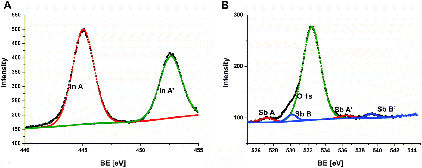 | ||
| Fig. 3 In 3d (A) and Sb 3d (B) XPS high resolution spectra of the InSb thin film obtained via electrodeposition. | ||
Seebeck coefficient (S) (Table 1) is found to be negative indicating that majority charge carriers are electrons (in freshly prepared InSb films). Nagata and Yamaguchi reported negative values of S for stoichiometric Si-doped InSb thin films formed by MOCVD.21 Depending on the degree of Si-doping, S was reported to vary from −217 μV K−1 to −178 μV K−1 for the wholly doped InSb thin film and Si-doped near the surface of InSb, respectively. The undoped indium antimonide thin film showed S at around −160 μV K−1. Our films exhibit a S value of −380 μV K−1, more than twice as high in comparison with the InSb obtained by MOCVD. Such a highly negative S value in the electrochemically prepared thin film is caused probably by considerable polycrystallinity, the presence of defects and vacancies formed during the synthesis.
| Nanocrystalline InSb thin film (1.5 μm in thickness) | n-InSb nanowire35 (67 nm in diameter, 8.5 μm in length) | |
|---|---|---|
| E g [eV] | 0.53 | 0.195 |
| n [cm−3] | 1.68 × 10¹⁷ | 4.74 × 10¹⁹ |
| σ [Ω−1 m−1] | 206 | 17.4 |
| μ [cm2 V−1 s−1] | 76.5 | 4.1 |
| Majority charge type | Electrons | Electrons |
| S [μV K−1] | −380 | — |
| P f [W m−1 K−2] | 2.97 × 10⁻⁵ | — |
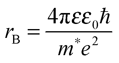
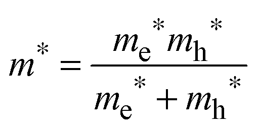
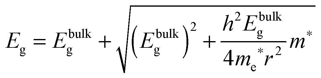
To determine the band gap of the obtained InSb films, FTIR analysis was performed. The recorded diffuse reflectance spectrum i.e. intensity vs. energy is shown in Fig. 4 as an Intensity = f(energy) function. The spectrum shows three characteristic features: an absorption onset at ca. 0.51 eV, a sharp peak at ca. 0.56 eV and a plateau at the high energy region. The 0.56 eV peak is attributed to the excitonic transition.22,23 A pure absorption spectrum was obtained by numerical subtraction of the excitonic Gaussian peak from the experimental spectrum. The resulting differential spectrum was used to create the Tauc plot (Fig. 4B). Due to the fact that InSb is a direct band gap semiconductor, the (KM·E)2 = f(E) relationship is plotted. The optical band gap of the value 0.53 eV was obtained from the linear fit of the low energy portion of the spectrum. The resulting value of Eg is much larger than that for bulk indium antimonide (0.17 eV at 300 K).13 There are two different factors that can be responsible for such behaviour: quantum confinement24 and Burstein–Moss shift.25 In order to check the possible role of the quantum confinement, the size of crystallites was estimated from the high resolution TEM images. The average value of d = 25 nm was found. On the other hand the Bohr radius of an exciton in InSb can be calculated from (1):
 | (1) |
 | (2) |
 | (3) |
 | (4) |
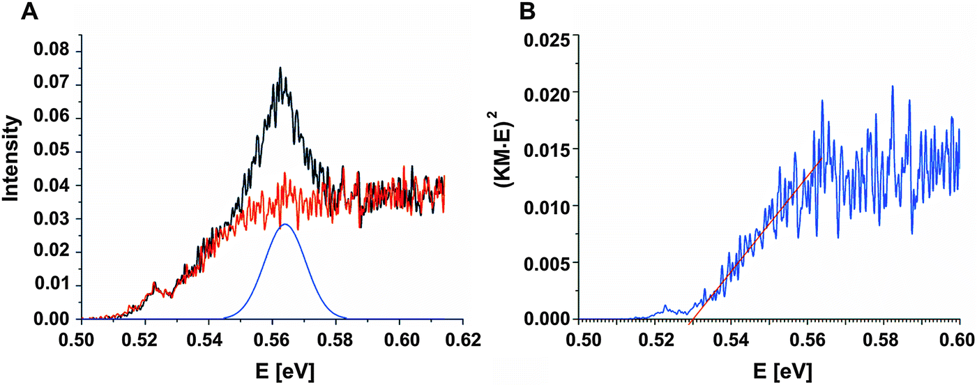 | ||
| Fig. 4 (A) FTIR spectrum of the InSb thin film: original spectrum (black), fitted excitonic peak (blue) and differential spectrum (red) together with (B) Tauc plot indicating the direct band gap (blue) with the linear fit (red) of the low energy portion of the spectrum. | ||
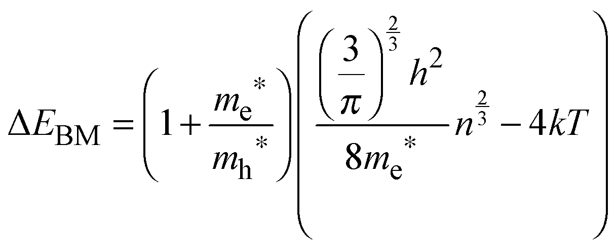
Assuming ΔEBM to be equal to 0.19 eV, on the basis of eqn (4), one can estimate the concentration of electrons n in the InSb thin film. The obtained n value of 1.68 × 1017 cm−3 is one order of magnitude higher than for bulk InSb (2 × 1016 cm−3). Therefore, it may be assumed that the band gap widening is associated with the size of crystallites and an increase in concentration of charge carriers via doping. Moreover, quantum confinement and the Burstein–Moss effect have rather a similar magnitude of 0.17 and 0.19 eV, respectively.
In order to learn more about the electrical properties of electrochemically deposited thin films, sheet resistance measurements were performed. The resulting conductivity values, as well as other electrical parameters for a freshly prepared InSb thin film measured at 294 K are presented in Table 1.
Electrical characteristics of n-InSb thin films synthesized via magnetron sputtering, electron beam evaporation, metalorganic vapour phase epitaxy and many other methods have been reported in the literature. Carrier concentrations of one order of magnitude smaller than our value (Table 1) were reported for InSb epitaxial layers grown by MBE29 (1.6 × 1016 cm−3), MOCVD30 (2.48 × 1016 cm−3) and for Pb-doped InSb thin films31 (1.6 × 1016 cm−3). It was also shown that higher n values can be obtained by doping InSb with Sn32 and Si33 atoms or by using radio frequency magnetron sputtering.34 Knowing the n determined from eqn (4) (under the assumption that only quantum confinement and the Burstein–Moss effect are involved in widening of the energy band gap) and the measured conductivity σ we estimated charges mobility μ (μ = σ/ne). The obtained value (76.5 cm2 V−1 s−1) is lower than the value determined for polycrystalline n-InSb films,34 monocrystalline layers8,30 and bulk materials. This fact can be explained by significant contribution of increased electron scattering at the grain boundaries.
For the electrochemically synthesized InSb thin film, the RT value of thermoelectric power factor (Pf = S2σ) was calculated (Table 1). The power factor is an important parameter often used to express the energy conversion efficiency. The calculated power factor for the as-deposited InSb film, with a stoichiometric composition, equals to 2.97 × 10⁻⁵ W m−1 K−2. Ishii et al.30 showed that a thin monocrystalline InSb film can reach a power factor of about 4.56 × 10⁻⁵ W m−1 K−2. This value is in good agreement with our results.
The influence of reducing the dimensionality from a film to a nanowire on the electric properties is shown in Table 1. It can be seen that the nanowires show a two orders of magnitude higher concentration of charge carriers than our thin films. This can be attributed to a significantly higher amount of defects, which is the characteristic feature for the nanowires obtained by electrochemical deposition. Due to the fact that nanowires are composed of crystals with a small diameter (a few nanometers), increased scattering at the grain boundaries explains the strong reduction of charge carrier mobility (μ) in comparison with a thin film obtained via the same synthesis method. Due to the non-directional growth of thin films (in comparison with nanowires grown inside porous anodic alumina templates), larger crystal grains and less number of vacancies/defects are observed, which result in higher electrical conductivity (less number of interfaces and grain boundaries and less scattering of charge carriers are observed). In summary, reducing the dimensionality of the material while maintaining the same synthesis conditions lead to lower conductivity and electron mobility and increase the concentration of charge carriers as a result of increased defects concentration and reduced grain sizes.
D Conclusions
InSb thin films with a stoichiometric composition were successfully formed by pulsed electrochemical deposition. It was shown that the stoichiometric thin films: (i) are polycrystalline, (ii) have a compact structure with a crystal size of 20–30 nm, (iii) exhibit n-type conductivity, and (iv) have a widened band gap. The observed increase in Eg from 0.17 eV for the bulk material to 0.53 eV for our film can be caused by two factors: quantum confinement and a Burstein–Moss shift. The contribution of both effects to the measured Eg was estimated to be 0.17 eV and 0.19 eV, respectively. The proposed electrochemical method allows to obtain high quality nanocrystalline InSb thin films with a Seebeck coefficient twice as high and a power factor of the same order as for the layers formed by expensive synthesis methods (e.g., MBE and MOCVD). It is therefore anticipated that the approach discussed in this article provides a cost-effective and time efficient alternative strategy for the synthesis of high quality InSb. Thus, it represents very important progress toward the development of more advanced materials and their potential application to, e.g., infrared detectors covering a broad spectral range.Acknowledgements
The study was supported by the Marian Smoluchowski Krakow Research Consortium “Matter-Energy-Future”, Leading National Research Centre (KNOW). The research was carried out with the equipment purchased thanks to the financial support of the Ministry of Science and Higher Education Iuventus Plus Program (project no. IP2014 0152 73) and the European Regional Development Fund in the framework of the Polish Innovation Economy Operational Program (Contract No. POIG.02.01.00-12-023/08).References
- R. K. Paul, S. Badhulika and A. Mulchandani, Appl. Phys. Lett., 2011, 99, 033103 CrossRef.
- K. Togawa, H. Sanbonsugi, A. Sandhu, M. Abe, H. Narimatsu, K. Nishio and K. H. Handa, Jpn. J. Appl. Phys., 2005, 44, L1494 CrossRef CAS.
- K. Togawa, H. Sanbonsugi, A. Lapicki, M. Abe, H. Handa and A. Sandhu, IEEE Trans. Magn., 2005, 41, 3661 CrossRef CAS.
- A. Rogalski, J. Appl. Phys., 2003, 93, 4355 CrossRef CAS.
- H. A. Nilsson, P. Caroff, C. Thelander, M. Larsson, J. B. Wagner, L.-E. Wernersson, L. Samuelson and H. Q. Xu, Nano Lett., 2009, 3151 CrossRef CAS PubMed.
- Y. R. Toda, K. S. Chaudhari, A. B. Jain and D. N. Gujarathi, Arch. Appl. Sci. Res., 2011, 3, 431 CAS.
- J. Y. Lim, J. D. Song, W. J. Choi, J. P. Ahn and H. S. Yang, Phys. Status Solidi A, 2011, 208, 2104 CrossRef CAS.
- J. Rahul, A. K. Verma, R. N. Tripathi and S. R. Vishwakarma, Mater. Sci. Polym., 2012, 30, 375 CrossRef.
- Y. Yao, C. Liu, H. Qi, X. Chang, C. Wang and G. Wang, Curr. Appl. Phys., 2011, 11, 620 CrossRef.
- S. Yamaguchi and M. Matsumoto, Vacuum, 2010, 84, 1323 CrossRef CAS.
- P. K. Chiang and S. M. Bedair, Appl. Phys. Lett., 1985, 46, 383 CrossRef CAS.
- G. D. Sulka, A. Brzózka and L. Liu, Electrochim. Acta, 2011, 56, 4972 CrossRef CAS.
- K. Hnida, J. Mech and G. D. Sulka, Appl. Surf. Sci., 2013, 287, 252 CrossRef CAS.
- G. D. Sulka, K. Hnida and A. Brzózka, Electrochim. Acta, 2013, 104, 536 CrossRef CAS.
- K. E. Hnida, R. P. Socha and G. D. Sulka, J. Phys. Chem. C, 2013, 117, 19382 CAS.
- M. S. Chandrasekar and M. Pushpavanam, Electrochim. Acta, 2008, 53, 3313 CrossRef CAS.
- X. Tang, R. G. V. Weltenis, F. M. V. Setten and A. J. Bosch, Semicond. Sci. Technol., 1986, 1, 355 CrossRef CAS.
- NIST X-ray Photoelectron Spectroscopy Database, Version 4.1 National Institute of Standards and Technology, Gaithersburg, 2012 http://srdata.nist.gov/xps/.
- S. Tanuma, C. J. Powell and D. R. Penn, Surf. Interface Anal., 1993, 21, 165 CrossRef.
- L. Liu, Z. Hu, Y. Cui, B. Li and X. A. Zhou, Solid State Sci., 2010, 12, 882 CrossRef CAS.
- H. Nagata and S. Yamaguchi, ESC Trans., 2009, 16, 7 CAS.
- J. F. Muth, J. H. Lee, I. K. Shmagin, R. M. Kolbas, H. C. Casey, P. B. Keller, U. K. Mishra and S. P. DenBaars, Appl. Phys. Lett., 1997, 71, 2572 CrossRef CAS.
- R. Winkler, Phys. Rev. B: Condens. Matter Mater. Phys., 1995, 51, 14395 CrossRef CAS.
- V. Kosacki, H. Petrovsky and U. Anderson, Appl. Phys. Lett., 1999, 3, 341 CrossRef.
- M. Bellardita, M. Addamo, A. Di Paola, L. Palmisano and A. M. Venezia, Phys. Chem. Chem. Phys., 2009, 11, 4084 RSC.
- L. E. Brus, J. Chem. Phys., 1984, 80, 4403 CrossRef CAS.
- Y. Wang, A. Suna, W. Mahler and R. Kasowski, J. Chem. Phys., 1987, 87, 7315 CrossRef CAS.
- B. Pejova and I. Grozdanov, Mater. Chem. Phys., 2005, 90, 35 CrossRef CAS.
- M. C. Debnath, T. D. Mishima, M. B. Santos, L. C. Phinney, T. D. Golding and K. Hossain, J. Vac. Sci. Technol., B, 2014, 32, 02C116 Search PubMed.
- T. Ishii, H. Homma and S. Yamaguchi, Adv. Mater. Res., 2011, 254, 50 CrossRef CAS.
- M. Oszwałdowski, T. Berus and V. K. Dugaev, Phys. Rev. B: Condens. Matter Mater. Phys., 2002, 65, 235418 CrossRef.
- S. Ishida, K. Takeda, A. Okamoto and I. Shibasaki, Physica E, 2004, 20, 211 CrossRef CAS.
- T. Zhang, J. J. Harris, W. R. Branford, S. K. Clowes, L. F. Cohen and S. A. Solin, Semicond. Sci. Technol., 2006, 21, 1543 CrossRef CAS.
- T. Zens, P. Bacla, A. M. Agarwal, L. C. Kimerling and A. Drehman, J. Cryst. Growth, 2011, 334, 84 CrossRef CAS.
- K. E. Hnida, S. Bäßler, L. Akinsinde, J. Gooth, K. Nielsch, R. P. Socha, A. Łaszcz, A. Czerwinski and G. D. Sulka, Nanotechnology, 2015, 25, 285701 CrossRef PubMed.
| This journal is © The Royal Society of Chemistry 2016 |