
 Open Access Article
 This Open Access Article is licensed under a
 Creative Commons Attribution 3.0 Unported Licence
Diamond-coated ‘black silicon’ as a promising material for high-surface-area electrochemical electrodes and antibacterial surfaces†
P. W.
May
 *a,
M.
Clegg
a,
T. A.
Silva
b,
H.
Zanin
c,
O.
Fatibello-Filho
b,
V.
Celorrio
a,
D. J.
Fermin
a,
C. C.
Welch
d,
G.
Hazell
e,
L.
Fisher
e,
A.
Nobbs
e and
B.
Su
e
*a,
M.
Clegg
a,
T. A.
Silva
b,
H.
Zanin
c,
O.
Fatibello-Filho
b,
V.
Celorrio
a,
D. J.
Fermin
a,
C. C.
Welch
d,
G.
Hazell
e,
L.
Fisher
e,
A.
Nobbs
e and
B.
Su
e
aSchool of Chemistry, University of Bristol, Bristol BS8 1TS, UK. E-mail: paul.may@bristol.ac.uk
bDepartamento de Química, Centro de Ciências Exatas e de Tecnologia, Universidade Federal de São Carlos, Rod. Washington Luís km 235, São Carlos CEP: 13560-970, SP, Brazil
cDepartamento de Componentes Semicondutores, Instrumentos e Fotônica, Faculdade de Engenharia Elétrica e de Computação da Universidade Estadual de Campinas, Av. Albert Einstein, 400, CEP 13081-970, Campinas, SP, Brazil
dOxford Instruments Plasma Technology, Yatton, Bristol BS49 4AP, UK
eSchool of Oral and Dental Sciences, University of Bristol, Lower Maudlin Street, Bristol, BS1 2LY UK
First published on 8th August 2016
Abstract
This report describes a method to fabricate high-surface-area boron-doped diamond (BDD) electrodes using so-called ‘black silicon’ (bSi) as a substrate. This is a synthetic nanostructured material that contains high-aspect-ratio nano-protrusions, such as spikes or needles, on the Si surface produced via plasma etching. We now show that coating a bSi surface composed of 15 μm-high needles conformably with BDD produces a robust electrochemical electrode with high sensitivity and high electroactive area. A clinically relevant demonstration of the efficacy of these electrodes is shown by measuring their sensitivity for detection of dopamine (DA) in the presence of an excess of uric acid (UA). Finally, the nanostructured surface of bSi has recently been found to generate a mechanical bactericidal effect, killing both Gram-negative and Gram-positive bacteria at high rates. We will show that BDD-coated bSi also acts as an effective antibacterial surface, with the added advantage that being diamond-coated it is far more robust and less likely to become damaged than Si.
A. Introduction
Diamond films grown by chemical vapour deposition (CVD) are finding an increasing number of applications due to the superlative properties of diamond coupled with their rising availability and affordability from a number of commercial suppliers.1 Doping the diamond with different amounts of boron allows the film conductivity to be varied from insulating to near-metallic.2 Highly conducting boron-doped diamond (BDD) films exhibit a number of properties that make them attractive for use as electrochemical electrodes; in particular they have a low background current, extreme electrochemical stability in both acidic and alkaline media, high resistance to fouling, and a wide potential window in aqueous solutions.3–8 These properties make BDD electrodes an exciting alternative to more traditional carbon allotrope electrodes such as glassy carbon, pyrolytic graphite and highly ordered pyrolytic graphite, making many electrochemical applications more attractive and viable.9,10 The pharmaceutical industry has begun utilising BDD electrodes for electroanalysis, which can be used to successfully detect a diverse range of biological molecules including caffeine,11 glucose,12 organic acids,13 serotonin and histamine,14 purines,15 and even cofactors such as nicotinamide adenine dinucleotide.16,17 BDD electrodes can also be used for water treatment and purification,18 for detecting trace amounts of contaminants in water via anodic stripping voltammetry,19 electrosynthesis of organic20 and inorganic21 compounds, neural interfacing,22,23 and the fabrication of supercapacitors.24The performance of BDD electrodes can often be greatly improved by modifying their size, shape and surface structure.25–29 In particular, structuring the diamond surface on the micro- or nano-scale has the effect of greatly increasing the effective electrode surface area, leading to higher sensitivity, increased selectivity, and higher capacitance values.30,31 Previous attempts to fabricate nanostructured BDD electrodes involved two approaches: either etching away areas of an existing BDD film or depositing the BDD onto an already structured scaffold.32 For the first approach, diamond can be etched using an O2-based reactive ion etch (RIE) process and a non-erodible mask made from metals (such as Al, Au, Mo or Ni), oxides (SiO2, Al2O3) or nanodiamond particles.33 Such techniques have allowed diamond electrodes to be etched into the form of nanopillars,34 nanowires,35 nanoneedles36,37 and nanowhiskers.38,39 In a similar way, extremely porous nanohoneycomb diamond structures have been produced by etching diamond films using an oxygen plasma through a porous alumina mask.40
The second approach involves diamond coating existing nanostructured substrates such as silicon25 or carbon nanotubes (CNTs) using CVD.41 Recently we reported that ‘forests’ of vertically aligned CNTs can be coated with nanocrystalline BDD, and in doing so, the CNTs clump together into bundles resembling ‘teepees’,42 as well as ridge, web and honeycomb structures.30 Such diamond-coated CNT nanostructures exhibited an increase in surface area and capacitance of up to 450 times when compared to flat BDD electrodes.30,43 The enhanced effectiveness and increased capacitance of diamond-coated CNT nanostructures make them suitable for multi-electrode array sensors for applications in neural prosthesis, neural stimulation, and brain-machine interfaces.22
Rather than coat CNTs, another approach is to pre-pattern the substrate material, usually Si, and then coat these micro/nanostructures with BDD. Peng and co-workers44 used an electroless metal deposition process to deposit micromasks onto a Si surface, which was then etched away leaving vertically aligned Si nanowires. These were then coated in BDD by CVD to produce a high-area electrode.25 The tips of the diamond ‘nanoforests’ were then electrochemically functionalized and consequently have been targeted for applications in biochemistry, in particular, as a non-enzymatic glucose sensor with high selectivity and stability.32
This report describes an alternative method to fabricate high-surface-area BDD electrodes using a different type of prepatterned Si. So-called ‘black silicon’ (bSi) is a synthetic nanostructured material that contains high-aspect-ratio nanoprotrusions, such as spikes or needles, on its surface produced through a simple plasma etching technique. An extensive review of plasma etching can be found in reference.45 The mechanism of bSi formation is believed to be simultaneous deposition of micromasks and anisotropic plasma etching of the Si surface.46–48 Originally something to be avoided, bSi has now found applications photovoltaics49–51 and later used for biomedical sensing applications.52,53 We now show that coating a bSi surface conformably with BDD produces a robust, sensitive electrode with high electroactive surface area. The electrochemical responses are initially assessed using a simple outer-sphere electron transfer probe (ferri/ferrocyanide).
However, a more clinically relevant test for the efficacy of these electrodes is to measure their sensitivity for detection of dopamine (DA) in the presence of an excess of uric acid (UA).54 DA is an important biomolecule which exists at very low concentrations in the body, but which plays an important role in the function of the central nervous, endocrine, cognition and emotion systems. Electrochemical methods have been used previously for determination of DA concentrations, however the coexistence of ascorbic acid (AA) and uric acid (UA) with similar oxidation potentials as DA, and at concentrations much higher than those of DA, cause overlapping voltammetric responses. Thus, a sensitive and accurate electrode for detection of DA in the presence of UA and/or AA is needed. Flat, traditional electrodes are nowhere near sensitive enough for simultaneous detection of DA, UA and AA. Therefore, modified materials such as metal nanoparticles and oxides, CNTs, and polymers, have been used to improve the selectivity, sensitivity, and stability of the electrode.54 We will demonstrate that BDD-coated bSi electrodes can also easily detect DA in the presence of UA.
Finally, the nanostructured surface of bSi has recently been found to generate a mechanical bactericidal effect, killing both Gram-negative and Gram-positive bacteria at high rates.55 We will show that BDD-coated bSi also acts as an effective antibacterial surface, with the added advantage that being diamond-coated it is far more robust and less likely to become damaged than Si.
B. Experimental
Black Si fabrication
Two types of bSi substrates were prepared by plasma etching of n-doped single-crystal silicon (100) wafers. Two different inductively coupled plasma (ICP) etching processes45 were used resulting in a bSi wafer of short needles (∼1 μm in length) and a wafer of long needles (∼15–20 μm in length), as shown in Fig. 1. The short needles were produced in an Oxford Instruments System 133 fitted with an ICP380 source. The conditions were Cl2 (48 sccm), O2 (2 sccm), 15 mTorr pressure, 600 W ICP power, 100 W reactive ion etch (RIE) bias power, 20 °C electrode, 10 min etching time. The long needles were formed in an Oxford Instruments System 100 fitted with a Cobra300 ICP source. A cryogenic etch47,48,56–58 was used as follows: SF6 (60 sccm), O2 (10 sccm), 10 mTorr pressure, 800 W ICP power, 6 W RIE power, −110 °C electrode, with 10 Torr He applied to the backside of the wafer for effective cooling, 30 min etching time. These long needles are some of the longest bSi features reported to date. Both these wafers were cleaved into multiple identical square samples ∼1 cm2 in size suitable for electrochemical testing.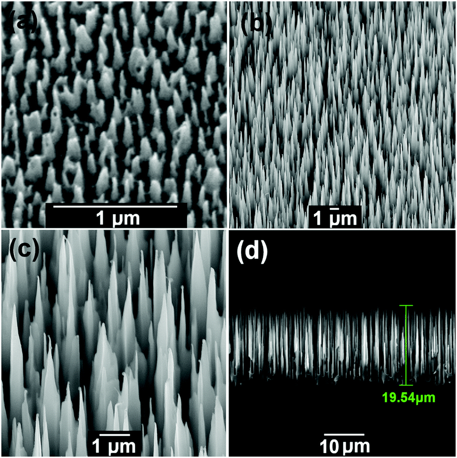 | ||
| Fig. 1 The two types of bSi before coating with diamond. (a) Short needles with length 0.5–1 μm. (b–d) Long needles with length 15–20 μm. | ||
Diamond deposition
The bSi samples were then seeded using a suspension of detonation nanodiamond (DND) in methanol using an electrospray process59 in which the DND suspension was placed under high potential difference (35 kV) with respect to the grounded sample. Due to electrostatic attraction the suspension sprayed onto the sample and coated all the surfaces, including the vertical sides of the needles, with a near monolayer of ∼10 nm DND seeds. The seeded samples were then placed into a hot filament CVD (HFCVD) reactor, and ∼0.25 μm of either (i) heavily boron-doped microcrystalline diamond (MCD), or (ii) heavily boron-doped nanocrystalline diamond (NCD), was deposited using standard CVD conditions: 20 Torr pressure, Ta filament at 2400 K, substrate temperature ∼900 °C, (i) 1%CH4/H2 gas mixture + 2000 ppm B2H6, (ii) 4%CH4/H2 gas mixture + 2000 ppm B2H6.1,2 The level of B doping was sufficient to ensure that in both types of film the diamond had near-metallic conductivity. The resulting diamond-coated bSi samples are shown in Fig. 2. Due to the heavy B doping and the submicron thickness of the diamond layer, the diamond grain size is small (<100 nm) so the MCD film appears rounded with only small facets visible. The NCD film appears even more rounded with no signs of facets. The short bSi needles were coated uniformly with diamond, leaving a surface which was slightly rounded compared to the uncoated needles (Fig. 2(a)). The long needles, however, became diamond coated conformally and uniformly all down their length, with complete coverage occurring after 1 h growth (Fig. 2(b and c) for MCD, and Fig. 2(e and f) for NCD). A further sample was fabricated by depositing NCD onto the long needles for 2 h, leading to the rounded diamond nanocrystallites beginning to fill in the spaces between the needles until they were almost, but not completely, encapsulated. This led to a highly porous but flatter film (Fig. 2(f and g)). Growth times >2 h led to non-porous diamond films with the bSi needles completely embedded within a solid diamond layer.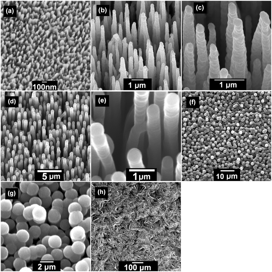 | ||
| Fig. 2 The two types of bSi after coating with BDD. (a) Short needles – the BDD-coated needles are more rounded than before. (b and c) Long needles – conformally coated with boron-doped MCD. (d and e) Long needles – conformally coated with smoother, more rounded boron-doped NCD. (f and g) The long needles are partially overgrown with boron-doped NCD, but there are still porous cavities allowing access to the interior of the film. (h) A ‘flat’ commercial BDD electrode used as a control. | ||
Other electrodes were prepared for comparison in the electrochemical tests. A standard commercial microcrystalline BDD sample (Element Six, electrochemical grade) was used as the control. This was essentially a flat electrode, although the surface had crystalline facets of size ∼20 μm (Fig. 2(f)).
Electrode fabrication
For use as the working electrode, the BDD-coated bSi and BDD flat samples were immobilized on a copper plate (1.0 × 1.0 cm2) using conductive silver paste and sealed using 2 different methods, depending upon which laboratory performed the experiments. For measurements conducted in Brazil, the electrodes were sealed with epoxy resin, leaving an area of about 8 × 8 mm of the BDD surface exposed. For measurements made in Bristol, Teflon tape with a 7 mm2 hole (which defined the geometrical area of the electrode) was placed on top of the samples leaving part of the electrode surface exposed at the corner of the sample with which to form an electrical connection. Conductive silver paint was applied to this region and copper tape applied on top (which was then connected to the potentiostat) before finally being covered in Teflon tape. This top connection was more reliable than a back connection, as it eliminated conduction through the Si substrate – however it still relied on there being full connectivity across the surface of the film from the exposed electrode area to the edge contact. The electrochemical results from both laboratories using the different sealing methods were almost identical, with the only difference being in the area of electrode exposed which determined the absolute magnitude of the measured current.Electrochemical analysis
The various electrodes were analysed electrochemically via cyclic voltammetry (CV) using two aqueous solutions: (i) a potassium nitrate solution (0.1 M) and (ii) a potassium ferricyanide (1 mM) with potassium chloride (0.1 M) supporting electrolyte solution, utilising a μAutolab Type III potentiostat. The electrolyte solution (20 ml) was placed into a glass three-electrode electrochemical cell along with the diamond working electrode, a Ag/AgCl (3.0 M KCl) reference electrode, and a Pt counter electrode. A conditioning step was applied before every scan which entailed applying the starting voltage for 120 s followed by a 10 s equilibration.Biomolecule analysis and detection
As the BDD-coated (Fig. 2(b and c)) and partially overgrown bSi long needle (Fig. 2(f and g)) samples had proven (see later) to be the most sensitive electrodes in the above KNO3 and ferri/ferrocyanide systems, these two electrodes were chosen for trials of DA and UA detection, with the usual flat (Element Six) BDD electrode as control. First their electrochemical response towards DA was determined using an aqueous 0.2 M phosphate buffer solution (pH = 7.0) containing 0.2 mM of DA. CVs were performed between −0.2 and +0.7 V at a variety of potential scan rates between 10 mV s−1 and 400 mV s−1. Then, linear sweep voltammograms were recorded in the same buffer solution but with varying concentrations of DA from 5.0 × 10⁻⁶ to 1.0 × 10⁻⁴ M to determine the analytical sensitivity of the different electrodes towards DA voltammetric sensing. These two experiments were then repeated with UA using the same buffer solution.Differential pulse voltammograms were then recorded in the same buffer solution with both DA and UA present, with (i) the UA concentration constant at 3.0 × 10⁻⁵ M while varying the DA concentration from 3.0 × 10⁻⁷ to 5.0 × 10⁻⁶ M, and (ii) the DA concentration constant at 3.0 × 10⁻⁶ M while varying the UA concentration from at 3.0 × 10⁻⁶ to 5.0 × 10⁻⁵ M. This was to ensure the electrode could detect the presence of one analyte in the presence of excess of the other. Finally, differential pulse voltammograms were recorded in the same buffer solution with both DA and UA present in varying concentrations. From these, the analytical parameters for the simultaneous voltammetric determination of DA and UA were recorded, including the linear concentration range, analytical sensitivity and limit of detection (LOD). The LODs were calculated using the relation 3σ/m, where σ is the standard deviation of ten blank (supporting electrolyte only) measurements and m is the slope of the analytical curve (analytical sensitivity). In addition, the stability of response of the proposed electrode material toward DA and UA detection was evaluated from repeatability studies.
Bactericidal surface testing
In this preliminary trial, only the short BDD-coated bSi needles were tested for their bactericidal properties. This was because literature reports on other structured surfaces suggest that spiky features of length ∼1 μm are optimal for cell destruction.60,61 Several 1 cm2 of the BDD-coated short-needle bSi samples fabricated as above were laser cut into quarters to provide 10 identical samples each of size 0.25 cm × 0.25 cm. These were then acid washed in concentrated sulfuric acid (>95%, 10 ml, 80 °C) for 30 min and then reterminated with hydrogen using H2 gas in a HFCVD reactor. This last step was to ensure that none of the oxygen termination that results from acid-cleaning diamond remained, as it is known that O-terminated diamond is an effective substrate for growth of many types of biological cells,62 and thus is the opposite of what we require in this case.Ten identical BDD films were deposited onto flat seeded Si samples to act as a control. The BDD was deposited using the same CVD conditions as before, except for a time of ∼8 h leading to a diamond film ∼4 μm thick. Due to the polycrystalline nature of the CVD process, the resulting diamond film was not perfectly flat, but was composed of facetted crystallites around 2 μm in size.
Each sample was then rinsed with absolute-ethanol before being submerged in 2 ml of a bacterial suspension (in a 12-well microtiter plate). The bacterium chosen was Pseudomonas aeruginosa, a common Gram-negative rod-shaped bacterium that is associated with disease in plants and animals including humans, such as pneumonia and various types of sepsis. It is currently of considerable medical importance because it is considered to be a prototypical multidrug resistant (MDR) pathogen with advanced antibiotic resistance.63 Bacteria culture preparation was conducted according to standard protocol.64 Briefly, P. aeruginosa ATCC 27853 was grown aerobically for 16 h in 10 ml Luria-Bertani broth (LBB, Sigma-Aldrich) in a 37 °C shaker set at 220 rpm. The bacterial suspension was then diluted in LBB to OD600 0.1 and further incubated until mid-exponential phase was reached. Bacterial cells were then harvested by centrifugation (7 min, 5000g), washed twice in 10 mM tris-HCl buffer (Sigma-Aldrich), and suspended in tris-HCl buffer to OD600 0.3 (approximately 107 cfu ml−1).
The samples were incubated in the bacterial suspension for 1 h at 37 °C under static conditions before being rinsed with tris-HCl buffer to remove any non-adherent bacteria. 1 ml of Live/Dead® BacLight™ bacterial viability stain (ThermoFisher Scientific) was then applied to each surface (as per manufacturers' instructions) followed by incubation at 25 °C for 15 min, followed by a final rinse using tris-HCl buffer. The prepared samples were then maintained in 1 ml of tris-HCl buffer whilst fluorescence microscopy was used to visualize the bacterial viability. This viability stain simultaneously stained viable cells with calcein-AM (green fluorescence) and dead cells with propidium iodide (red fluorescence) solutions. Viable cells took up the lipophilic SYTO 9 and metabolized it into the fluorescent calcein, resulting in green fluorescence from only viable cells. In contrast, propidium iodide struggled to transpose a viable cell membrane and instead could only pass through the more disordered regions of a dead cell membrane, resulting in red fluorescence only in dead cells. ImageJ Software was then used to manually count the number of green- and red-stained cells and thereby quantify the number of bacterial cells with an intact cell membrane (viable) and a damaged cell membrane (dead). A two-tailed homoscedastic Student's t-test was performed to compare data sets. If the p value was less than 0.05, then results were statistically significant.
For SEM imaging, following incubation with P. aeruginosa, surfaces were fixed by immersion in a 2.5% v/v glutaraldehyde solution (Sigma Aldrich) dissolved in 0.1 M phosphate buffer (potassium phosphate monobasic and potassium phosphate dibasic, pH 7.2, Sigma Aldrich) for 2 h at room temperature. An alcohol dehydration stage was then performed by immersing the surfaces in 20%, then 40%, 60%, 80% and 100% ethanol for 10 min each prior to 10 min in hexamethyldisilazane (Sigma Aldrich). Surfaces were then air dried, mounted onto carbon stubs and sputtered twice with gold for 1 min each time. A Helios Nanolab 600 combined with FIB-SEM was used to visualize the surfaces.
C. Results
Material characterisation
Laser Raman spectra of the BDD MCD coated substrates showed the characteristic peaks associated with heavily boron-doped thin diamond films, namely the graphitic D and G bands from the sp2 carbon at grain boundaries, the small, broadened diamond peak which is shifted and asymmetric due to Fano resonance,2 and peaks at 500 cm−1 and ∼1200 cm−1 related to boron incorporation (see Fig. 3). The Si 1st-order peak at ∼520 cm−1 is obscured by the large B2 feature, but the second order can be seen as a broad feature around 950 cm−1.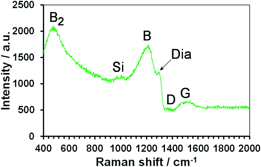 | ||
| Fig. 3 Raman spectra of the BDD-coated long-needle sample using green (514 nm) excitation. Label key: Dia is the diamond peak, D & G are the disordered and ordered sp2 carbon bands, respectively, Si is the second-order peak from the bSi substrate, B and B2 are peaks due to boron and boron-dimer incorporation, respectively. | ||
Electrochemical performance
Cyclic voltammograms were first recorded only in the presence of background electrolyte solution (KNO3), recording the capacitive current at a range of scan rates. The CVs recorded for the different electrode types all appeared quasi-rectangular in shape (see ESI†) characteristic of interfacial double-layer (DL) charging.65,66 The DL charging current is proportional to the active surface area of the electrode. There is significant difference in the capacitive current of the various BDD electrodes compared with that from the flat sample (see Table 1). This is not surprising, as DL charging is most apparent in systems with a large surface-area-to-volume ratio, as in materials with structures on the scale of μm to nm.67 The largest DL capacitive current was produced by the partially overgrown BDD-coated long needles, followed by the BDD-coated long needles, and finally the BDD-coated short needles whose current differed negligibly from that of the flat BDD electrode. There was no significant difference in behaviour between MCD and NCD-coated electrodes of either type. Therefore, we concluded that the surface topology of the electrodes is more important than the minor differences in grain size and sp2 carbon content between MCD and NCD. Assuming that for the flat diamond substrate the effective surface area and the geometric surface area were approximately equal, the effective surface area of each nanostructured electrode was then calculated from the ratio of the capacitances (also shown in Table 1).| Electrode | Capacitance/(μF cm−2) | Relative effective surface area |
|---|---|---|
| Flat BDD (Element Six) | 2.9 | 1.0 |
| BDD-coated bSi short needles | 7.6 | 2.6 |
| BDD-coated bSi long needles | 279.4 | 97 |
| Partially overgrown BDD-coated bSi long needles | 638.0 | 221 |
The performance of the electrodes was then analysed in the presence of 1 mM K3[Fe(CN)6], which resulted in CVs with the characteristic oxidation and reduction peaks as shown in Fig. 4. The peak-to-peak potential separation (ΔEp) and the peak current density appear to be dependent on the diamond microstructure. As discussed in previous papers,30,68 these two parameters exhibit a complex dependence on the electrode microstructure, particularly in the case of high-surface-area electrodes. For instance, the decrease in ΔEp with increasing electrode roughness reflects a decrease in the phenomenological charge-transfer resistance associated with electron transfer events. This could be connected to the increase in the effective surface area or to active sites exhibiting faster transfer kinetics. In the case that the dimensions of the electrode porosity are comparable to the diffusion layer thickness, ΔEp will decrease below the 59 mV associated with planar diffusion profiles. On the other hand, the increase in the peak current density with increasing roughness is primarily due to the increase in the background capacitive current and, to a lesser extent, to a decrease in the charge-transfer resistance. It is important to clarify that the peak current density for outer-sphere redox probes is determined by the geometric rather than the specific surface area. The reversibility of the redox probe is determined by the square-root dependence of the peak current with the potential scan rate as illustrated in Fig. 4(b). A more detailed analysis of the dynamic electrochemical responses is beyond the scope of this work. However, the data illustrated in Fig. 4 demonstrate the excellent charge transport properties in these complex diamond electrodes and their suitability for electroanalysis.
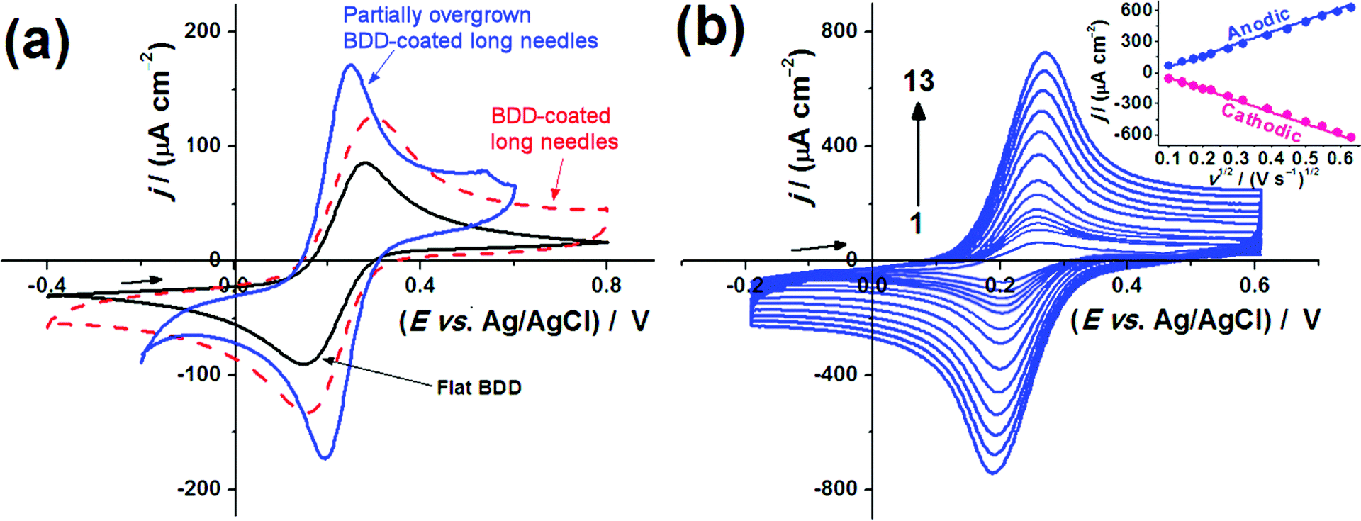 | ||
| Fig. 4 (a) CVs recorded in 0.1 M KCl solution containing 1 mM K3[Fe(CN)6] at a fixed scan rate of 50 mV s−1 using electrodes made from commercial flat BDD, BDD-coated bSi long needles and partially overgrown BDD-coated bSi long needles. (b) An example of a set of 13 CVs recorded at different scan rates (1: 10 mV s−1 to 13: 400 mV s−1), in this case for the partially overgrown long BDD-coated bSi needles. Inset: Plots of anodic and cathodic peak current densities vs. v1/2. | ||
The two most sensitive electrodes, the BDD-coated and partially overgrown bSi long-needle samples, were then used for analysis of DA in the presence of UA. Fig. 5(a) shows CVs for DA in buffer solution for the 2 BDD-coated bSi electrodes compared to the flat BDD control. The high-surface-area electrodes lead to a sharp increase in the current response and a shift of the anodic current peak potential towards less positive values with respect to the flat BDD electrode. As opposed to ferrocyanide, DA requires adsorption to the electrode surface prior to the oxidation step (i.e. an inner-sphere electron transfer). Consequently, changes in the effective surface area will have a more significant impact on the phenomenological charge-transfer resistance and the voltammetric responses. Again, in the case of the bSi long needle electrode, the changes in the electrochemical kinetics are rather stark, leading to a reversible electrochemical response at a wide range of potential scan rates (Fig. 5(b)).
 | ||
| Fig. 5 (a) CVs recorded in 0.2 M phosphate buffer solution (pH = 7.0) for 2.0 × 10⁻⁴ M DA using flat BDD, BDD-coated long needles, and partially overgrown BDD-coated long needles. Potential scan rate = 50 mV s−1. (b) An example of a set of CVs recorded at 13 different scan rates (1: 10 mV s−1 to 13: 400 mV s−1) in the same buffer solution as before containing 2.0 × 10⁻⁴ M of DA. This data set was recorded using the BDD-coated bSi long needle electrode. | ||
The analytical sensitivity of the two BDD electrodes toward DA voltammetric sensing was tested by the construction of analytical curves obtained by linear sweep voltammetry (LSV). Fig. 6(a) shows an example of LSVs recorded for different DA concentrations, in this case using the BDD-coated bSi long-needle electrode. The linear response to concentration can be seen in Fig. 6(b) for the three electrodes in question, along with their relative sensitivities. The following values of analytical sensitivity were recorded: 0.21 A cm−2 M−1 (flat BDD); 0.52 A cm−2 M−1 (BDD-coated bSi long needles) and 0.57 A cm−2 M−1 (partially overgrown BDD-coated bSi long needles). Therefore, the analytical sensitivity increased significantly with the use of the microstructured BDD electrodes, and the best analytical sensitivity was recorded using the partially overgrown BDD-coated bSi long-needle electrode.
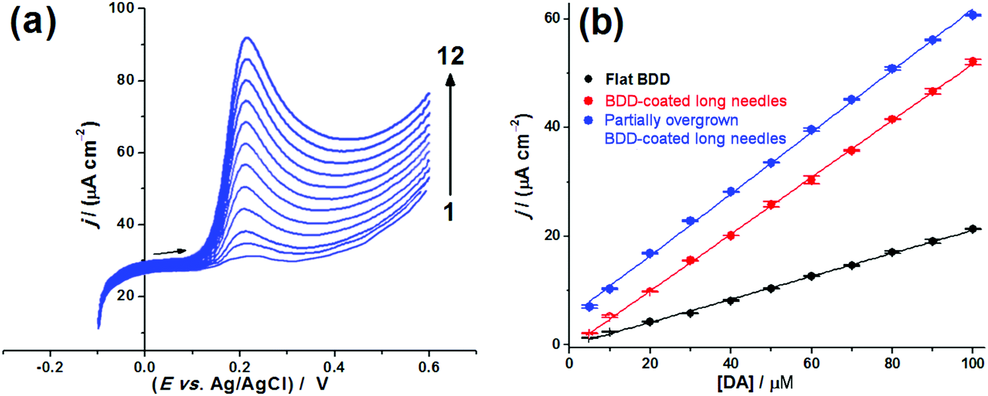 | ||
| Fig. 6 (a) LSVs recorded in 0.2 M phosphate buffer solution (pH = 7.0) containing 12 different DA concentration levels (1: 0.0 (blank solution) to 12: 1.0 × 10⁻⁴ M) using the BDD-coated bSi long needles, at a fixed potential scan rate of 100 mV s−1. (b) Linear response of current signal against DA concentration for the two BDD-coated bSi electrodes and the flat BDD control. The equations for the best fit lines of j (μA cm−2) vs. [DA] (μM) and correlation coefficients, r, are: flat BDD j = −0.059 + 0.21[DA], r = 0.999; BDD-coated long needles j = −0.47 + 0.52[DA], r = 0.999; partially overgrown BDD-coated long needles j = 5.1 + 0.57[DA], r = 0.999. | ||
Voltammetric testing of the performance of the electrodes towards UA detection was also undertaken, with broadly similar results to those from DA. The data and CV curves for the UA analysis can be found in the ESI.†
For the simultaneous voltammetric sensing of DA and UA, differential pulse voltammetry (DPV) was selected as a more sensitive voltammetric technique. Initially, the possible interference of one analyte on the response of the other was evaluated. For this, analytical curves were constructed maintaining one of the analytes at a fixed concentration. Fig. 7(a) shows the DPVs obtained in the presence of UA at fixed concentration (3.0 × 10⁻⁵ M) and DA with concentration ranging from 3.0 × 10⁻⁷ to 5.0 × 10⁻⁶ M. The DA response was linear over a wide concentration range in the presence of UA (inset of Fig. 7(a)), and the peak current densities recorded for UA showed a low relative standard deviation of 1.02%. This result proves that DA sensing did not interfere with the UA response. The same test was performed maintaining DA at fixed concentration of 3.0 × 10⁻⁶ M while varying the UA concentration from 3.0 × 10⁻⁶ M to 5.0 × 10⁻⁵ M, as shown in Fig. 7(b). Again, the electrode response toward UA was linear in the presence of DA (inset of Fig. 7(b)), and DA peak current densities showed a RSD of 5.82%, demonstrating the non-interference of UA sensing on the DA response.
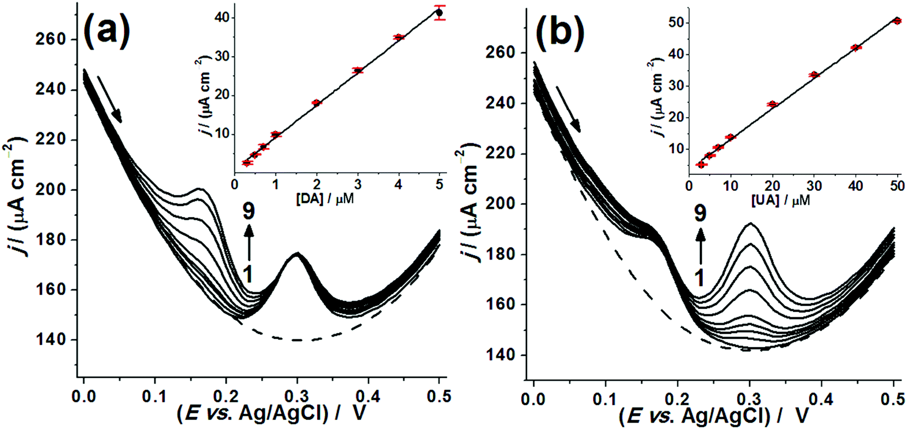 | ||
| Fig. 7 (a) DPVs recorded in 0.2 M phosphate buffer solution (pH = 7.0) for 3.0 × 10⁻⁵ M UA and different DA concentration levels (1: 0.0 (blank solution) to 9: 5.0 × 10⁻⁶ M) using the BDD-coated bSi long-needle electrode. Inset: Current density j (μA cm−2) vs. concentration of DA (μM) with linear best-fit equation j = 0.9 + 8.3[DA] and correlation coefficient r = 0.999. (b) DPVs recorded in 0.2 M phosphate buffer solution (pH = 7.0) for 3.0 × 10⁻⁶ M DA and different UA concentration levels (1: 0.0 (blank solution) to 9: 5.0 × 10⁻⁵ M) using the BDD-coated bSi long-needle electrode. Inset: Current density j (μA cm−2) vs. concentration of UA (μM) with linear best-fit equation j = 3.5 + 0.97[UA] and correlation coefficient r = 0.998. | ||
Next, the simultaneous analytical curves for DA and UA were constructed using the BDD-coated bSi long-needle electrode. Fig. 8(a) shows DPVs with both DA and UA present and while the concentrations of both are varied. The oxidation peaks are well separated and easily distinguishable over a large concentration range of both the two analytes. Fig. 8(b) and (c) show linear responses with concentration for DA and UA, respectively. From the analytical curves shown in Fig. 8(b) and (c), the analytical parameters for the simultaneous voltammetric determination of DA and UA were recorded, and these are given in Table 2. Thus, high analytical sensitivities and low LODs were achieved using the BDD-coated bSi long-needle electrode as an electrochemical sensor. The DPVs were repeated several times to determine the repeatability of the system. For this, ten successive DPV measurements (n = 10) were conducted on a buffer solution containing DA and UA at two different concentration levels: (1) [DA] = 1.0 μM and [UA] = 3.0 μM; (2) [DA] = 10.0 μM and [UA] = 30.0 μM. For the analytes at the lower end of their concentration ranges, the RSD obtained for peak current densities was ∼0.65% for DA and ∼1.1% for UA, while at the higher end of their concentration ranges the RSD reduced to ∼0.51% for DA and ∼0.53% for UA, respectively. These results demonstrate the high precision of measurement and stability of response of the proposed BDD electrodes.
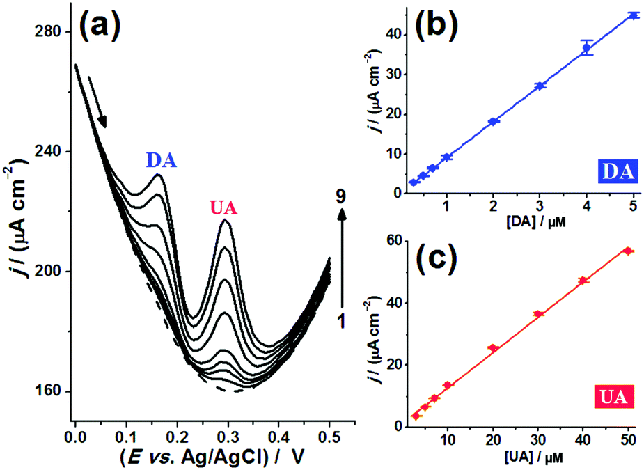 | ||
| Fig. 8 (a) DPVs recorded in 0.2 M phosphate buffer solution (pH = 7.0) containing 9 different DA and UA concentration levels (1: 0.0 (blank solution) to 9: 5.0 × 10⁻⁶ M of DA and 1: 0.0 (blank solution) to 9: 5.0 × 10⁻⁵ M of UA) using the BDD-coated bSi long-needle electrode. (b) Current density (μA cm−2) vs. concentration of DA (μM) with linear best-fit equation: j = 0.16 + 9.0[DA] and correlation coefficient 0.999. (c) Current density (μA cm−2) vs. concentration of UA (μM) with linear best-fit equation: j = 1.4 + 1.1[UA] and correlation coefficient 0.998. | ||
| DA | UA | |
|---|---|---|
| Range/μM | 0.30–0.50 | 3.0–50 |
| Analytical sensitivity/(μA cm−2 M−1) | 9.0 | 1.1 |
| LOD/μM | 0.27 | 2.1 |
Bactericidal properties
Turning now to the bactericidal properties of the structured BDD surface, both the BDD surface and a control ‘flat’ surface (actually a facetted surface with 2 μm crystallites, as described previously) were exposed to high numbers of exponential phase P. aeruginosa for 1 h and their bactericidal effects assessed using Live/Dead staining. Typical fluorescence micrographs are shown in Fig. 9, in which cells with intact membranes are stained in green while cells with damaged membranes are stained red. The nanopatterned BDD surface showed a significantly higher (p < 0.001) proportion of membrane-damaged cells with very few red cells present on the control surface. Both control and nanopatterned surfaces tested found comparable numbers of cells (p > 0.05) (Fig. 10(a)) and the percentage of stained dead cells is shown in Fig. 10(b). The nanopatterned BDD surface resulted in significant bacterial killing compared to the control surface. The overall number of dead cells on the control was ∼2%, compared to ∼13% on the BDD-coated short needle sample. Because both types of sample had diamond coatings with identical boron-doping levels and crystallinity, the enhanced cell death rate must be primarily due to the needle-shaped structured surface. Indeed, the increased cell death rate on the BDD-coated needle samples is comparable to that reported on other nanostructured antibacterial surfaces.69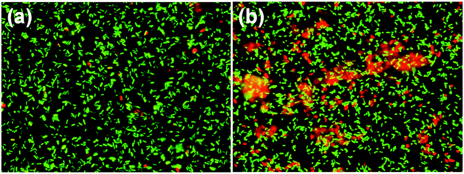 | ||
| Fig. 9 Fluorescence micrographs of P. aeruginosa after 1 h incubation on (a) a control ‘flat’ BDD sample and (b) a BDD-coated bSi short-needle sample. | ||
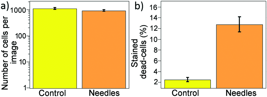 | ||
| Fig. 10 Total numbers of (a) bound bacteria and (b) percentage dead cells after 1 h incubation of P. aeruginosa on a control ‘flat’ BDD surface and a BDD-coated bSi short-needle surface, and subsequent viability determination by Live/Dead BacLight stain. | ||
Viability staining was also coupled with SEM imaging where equivalent samples were fixed after 1 h bacterial adhesion, as shown in Fig. 11. On the ‘flat’ BDD-coated substrates, cells adhered horizontally and appeared to remain in a healthy state (turgid), correlating with results from fluorescence microscopy experiments. This is in contrast to the BDD-coated bSi short-needles where a proportion of the cells appeared to be damaged by the nanofeatures, appearing flat and non-turgid. Thus, the greater non-uniformity of the surface appeared to effectively damage a higher percentage of the bacterial cells consistent with the results from the Live/Dead assays.
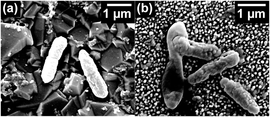 | ||
| Fig. 11 Example SEM images of P. aeruginosa after 1 h incubation on (a) ‘flat’ BDD surface and (b) BDD-coated short-needle surface. Image (a) shows healthy (turgid) bacterial cells, whereas image (b) shows damaged cells. | ||
D. Conclusions
We have demonstrated that coating bSi needles with BDD produces electrodes that have a high surface area which imparts high sensitivity to detection and measurement of analytes in aqueous solutions. Because the electrode active surface is diamond, all the usual advantages of diamond electrodes also apply to these electrodes – they are hardwearing and robust, have a large potential window, are resistant to fouling, etc., and these benefits are now combined with the economic advantages of being relatively cheap and easy to fabricate.Electrochemical data show that underlying charge transport properties of the microstructured diamond electrodes are not affected by the length of the needles, opening the possibility of fabricating microstructured diamond electrode arrays on bSi needles with lengths greater than 15 μm. On the other hand, the partially overgrown long needles exhibited the highest effective surface area, even if electron micrographs suggest partial coalescence of the diamond deposit. This behaviour suggests that short diamond deposition times lead to discontinuous coating and electrically isolated segments of the electrode.
The typical double-layer capacitance values for most carbon electrodes are of the order of 5 μF cm−2,70 whereas the BDD-coated long bSi needles had capacitance values of 280 μF cm−2 while the partially overgrown ones had values ∼640 μF cm−2. Such high capacitance values might make these electrodes suitable for use in supercapacitor applications. Moreover, the fact that the capacitance is a function of the bSi needle length suggests that the electrode capacitance can be tuned for different applications by simply changing the etch time used to create the bSi needles.
We showed that these electrodes can be used to distinguish DA in the presence of excess UA, with sensitivities and LOD values consistent with values from other nanostructured electrodes.54 The BDD-coated bSi short needles proved to have good anti-bacterial properties, killing around 13% of the cells that were placed upon this surface after only 1 h incubation. This cell-death rate is comparable to those from other nanostructured surfaces57,64 and to uncoated bSi.55 However, the advantage of the BDD coating is that it makes the surface far more robust and scratch-resistant. Sharp bSi needles can easily be scraped off the Si surface, and may then float in the air where they might be inhaled – with possible unwanted (and so far, unknown) health implications. This is far less likely with a diamond-coated bSi surface due to the hardness of the coating.
In this study, we only tested the short bSi needles for bactericidal properties. Having shown a positive result, the next steps will be to test diamond-coated bSi needles with a range of different lengths to determine the optimal needle length for maximum cell death, while maintaining a scratch-resistant surface. Although the focus of the report has been on bSi, it is clear that diamond-coating any micro- or nanostructured surface could be a useful way to protect that surface from mechanical damage while retaining its required abilities. Thus, we might envision a range of other otherwise delicate nanostructured surfaces and materials optimised for, say, anti-bacterial properties, for which a protective thin diamond coating could be the key to their wide-scale use.
Acknowledgements
The authors wish to thank the Electron Microscope Unit at the University of Bristol, School of Chemistry, for use of their facilities. PWM & HZ thank the Royal Society Newton Fund (grant number NI140181) for travel funds to make this UK/Brazil collaboration possible. DJF acknowledges the support by the Institute of Advanced Studies of the University of Bristol, (University Research Fellowship 2015). VC & DJF are also grateful or resources and financial support through the UK Catalysis Hub Consortium (EPSRC grants EP/K014706/1, EP/K014668/1, EP/K014854/1, EP/K014714/1 and EP/M013219/1). The authors also thank the EPSRC BristolBridge award: Bridging the Gaps between the Engineering and Physical Sciences and Antimicrobial Resistance (grant EP/M027546/1) for funding the trials of antimicrobial surfaces.References
- P. W. May, Philos. Trans. R. Soc. London, Ser. A, 2000, 358, 473 CrossRef CAS.
- P. W. May, W. J. Ludlow, M. Hannaway, P. J. Heard, J. A. Smith and K. N. Rosser, Diamond Relat. Mater., 2008, 17, 105 CrossRef CAS.
- M. Hupert, A. Muck, R. Wang, J. Stotter, Z. Cvackova, S. Haymond, Y. Show and G. M. Swain, Diamond Relat. Mater., 2003, 12, 1940 CrossRef CAS.
- Y. V. Pleskov, Russ. J. Electrochem., 2002, 38, 1275 CrossRef CAS.
- K. Peckova, J. Musilova and J. Barek, Crit. Rev. Anal. Chem., 2009, 39, 148 CrossRef CAS.
- M. H. Chen, G. T. Wu, G. M. Zhu, J. K. You and Z. G. Lin, J. Solid State Electrochem., 2002, 6, 420 CrossRef CAS.
- X. Tong, M. Liu and G. Zhao, J. Solid State Electrochem., 2010, 14, 221 CrossRef CAS.
- M. M. Villalba and J. Davis, J. Solid State Electrochem., 2008, 12, 1245 CrossRef CAS.
- S. G. Park, G. S. Kim, J. E. Park, Y. Einaga and A. Fujishima, J. New Mater. Electrochem. Syst., 2005, 8, 65 CAS.
- J. V. Macpherson, Phys. Chem. Chem. Phys., 2015, 17, 2935 RSC.
- N. Spataru, B. V. Sarada, D. A. Tryk and A. Fujishima, Electroanalysis, 2002, 14, 721 CrossRef CAS.
- C. E. Troupe, I. C. Drummond, C. Graham, J. Grice, P. John, J. I. B. Wilson, M. G. Jubber and N. A. Morrison, Diamond Relat. Mater., 1998, 7, 575 CrossRef CAS.
- O. Chailapakul, E. Popa, H. Tai, B. V. Sarada, D. A. Tryk and A. Fujishima, Electrochem. Commun., 2000, 2, 422 CrossRef CAS.
- B. V. Saranda, T. N. Rao, D. A. Tryk and A. Fujishima, Anal. Chem., 2000, 72, 1632 CrossRef.
- E. Popa, D. A. Tryk and A. Fujishima, Diamond Materials VI, 2000, 99, 512 Search PubMed.
- R. Channon, M. Joseph, E. Bitziou, A. Bristow, A. Ray and J. Macpherson, Anal. Chem., 2015, 87, 10064 CrossRef CAS PubMed.
- G. Mansano, A. Eisele, L. Dall'Antonia, S. Afonso and E. Sartori, J. Electroanal. Chem., 2015, 738, 188 CrossRef CAS.
- J. Utrilla, M. Polo, M. García, G. Joya and R. Pérez, Chemosphere, 2013, 93, 1268 CrossRef PubMed.
- E. A. McGaw and G. M. Swain, Anal. Chim. Acta, 2006, 575, 180 CrossRef CAS PubMed.
- J. Iniesta, P. A. Michaud, M. Panizza, G. Cerisola, A. Aldaz and C. Comninellis, Electrochim. Acta, 2001, 46, 3573 CrossRef CAS.
- M. S. Saha, T. Furuta and Y. Nishiki, Electrochem. Solid-State Lett., 2003, 6, D5 CrossRef CAS.
- G. Piret, C. Hébert, J.-P. Mazellier, L. Rousseau, E. Scorsone, M. Cottance, G. Lissorgues, M. O. Heuschkel, S. Picaud, P. Bergonzo and B. Yvert, Biomaterials, 2015, 53, 173 CrossRef CAS PubMed.
- A. C. Taylor, B. Vagaska, R. Edgington, C. Hébert, P. Ferretti, P. Bergonzo and R. B. Jackman, J. Neural Eng., 2015, 12, 066016 CrossRef PubMed.
- S. Yu, N. Yang, H. Zhuang, J. Meyer, S. Mandal, O. A. Williams, I. Lilge, H. Schönherr and X. Jiang, J. Phys. Chem. C, 2015, 119, 18918 CAS.
- D. B. Luo, L. Z. Wu and J. F. Zhi, ACS Nano, 2009, 3, 2121 CrossRef CAS PubMed.
- M. Lv, M. Wei, F. Rong, C. Terashima, A. Fujishima and Z. Z. Gu, Electroanalysis, 2010, 22, 199 CrossRef CAS.
- A. Ay, V. M. Swope and G. M. Swain, J. Electrochem. Soc., 2008, 155, B1013 CrossRef CAS.
- N. A. Braga, C. A. A. Cairo, J. T. Matsushima, M. R. Baldan and N. G. Ferreira, J. Solid State Electrochem., 2010, 14, 313 CrossRef CAS.
- D. Luo and J. Zhi, Electrochem. Commun., 2009, 11, 1093 CrossRef CAS.
- H. Zanin, P. W. May, D. J. Fermin, D. Plana, S. M. C. Vieira, W. I. Milne and E. J. Corat, ACS Appl. Mater. Interfaces, 2013, 6, 990 Search PubMed.
- N. Yang, H. Uetsuka, O. A. Williams, E. Osawa, N. Tokuda and C. E. Nebel, Phys. Status Solidi A, 2009, 206, 2048 CrossRef CAS.
- Y. Yu, L. Wu and J. Zhi, in Diamond Nanowires: Fabrication, Structure, Properties and Applications in Novel Aspects of Diamond from Growth to Applications, ed. N. Yang, Springer International, Switzerland, 2015, ch. 5, pp. 123–164 Search PubMed.
- H. Li, S. Cheng, J. Li and J. Song, J. Nanomater., 2015, 2015, 692562 Search PubMed.
- Y. S. Zou, Y. Yang, W. J. Zhang, Y. M. Chong, B. He, I. Bello and S. T. Lee, Appl. Phys. Lett., 2008, 92, 053105 CrossRef.
- N. Yang, H. Uetsuka and C. E. Nebel, Adv. Funct. Mater., 2009, 19, 887 CrossRef CAS.
- C. Lu, Y. Li, S. Tian, W. Li, J. Li and C. Gu, Microelectron. Eng., 2011, 88, 2319 CrossRef CAS.
- Y. Yang, M. Yuen, X. Chen, S. Xu, Y. Tang and W. Zhang, CrystEngComm, 2015, 17, 2791 RSC.
- C. Y. Li and A. Hatta, Diamond Relat. Mater., 2006, 15, 357 CrossRef CAS.
- C. Y. Li and A. Hatta, Jpn. J. Appl. Phys., 2006, 45, 8378 CrossRef CAS.
- H. Masuda, M. Watanabe, K. Yasui, D. Tryk, T. Rao and A. Fujishima, Adv. Mater., 2000, 12, 444 CrossRef CAS.
- Q. Yang, W. Chen, C. Xiao, A. Hirose and R. Sammynaiken, Diamond Relat. Mater., 2005, 14, 168 Search PubMed.
- Y. Zou, P. W. May, S. M. C. Vieira and N. A. Fox, J. Appl. Phys., 2012, 112, 044903 CrossRef.
- B. C. Lourencao, T. A. Silva, H. Zanin, P. W. May, E. J. Corat and O. Fatibello-Filho, J. Solid State Electrochem., 2016 DOI:10.1007/s10008-016-3128-4.
- K. Peng, Y. Yan, S. Gao and J. Zhu, Adv. Mater., 2002, 14, 1164 CrossRef CAS.
- V. M. Donnelly and A. Kornblit, J. Vac. Sci. Technol., A, 2013, 31, 050825 Search PubMed.
- H. Jansen, M. de Boer, R. Legtenberg and M. Elwenspoek, J. Micromech. Microeng., 1995, 5, 115 CrossRef CAS.
- H. V. Jansen, M. J. de Boer, S. Unnikrishnan, M. C. Louwerse and M. C. Elwenspoek, J. Micromech. Microeng., 2009, 19, 033001 CrossRef.
- I. W. Rangelow, J. Vac. Sci. Technol., A, 2003, 21, 1551 Search PubMed.
- J. Oh, H. C. Yuan and H. M. Branz, Nat. Nanotechnol., 2012, 7, 743 CrossRef CAS PubMed.
- H. C. Yuan, V. E. Yost, M. R. Page, P. Stradins, D. L. Meier and H. M. Branz, Appl. Phys. Lett., 2009, 95, 123501 CrossRef.
- X. Liu, P. R. Coxon, M. Peters, B. Hoex, J. M. Cole and D. J. Fray, Energy Environ. Sci., 2014, 7, 3223 CAS.
- W. Kim, J. K. Ng, M. E. Kunitake, B. R. Conklin and J. Yang, J. Am. Chem. Soc., 2007, 129, 7228 CrossRef CAS PubMed.
- A. K. Shalek, J. T. Robinson, E. S. Karp, J. S. Lee, D.-R. Ahn, M.-H. Yoon, A. Sutton, M. Jorgolli, R. S. Gertner, T. S. Gujral, G. MacBeath, E. G. Yang and H. Park, Proc. Natl. Acad. Sci. U. S. A., 2010, 107, 1870 CrossRef CAS PubMed.
- S. Mahshid, C. Li, S. S. Mahshid, M. Askari, A. Dolati, L. Yang, S. Luoa and Q. Cai, Analyst, 2011, 136, 2322 RSC.
- E. P. Ivanova, J. Hasan, H. K. Webb, G. Gervinskas, S. Juodkazis, V. K. Truong, A. H. F. Wu, R. N. Lamb, V. A. Baulin, G. S. Watson, J. A. Watson, D. E. Mainwaring and R. J. Crawford, Nat. Commun., 2013, 4, 2838 Search PubMed.
- C. C. Welch, A. L. Goodyear, T. Wahlbrink, M. C. Lemme and T. Mollenhauer, Microelectron. Eng., 2006, 83, 1170 CrossRef CAS.
- D. H. Henry, C. C. Welch and A. Scherer, J. Vac. Sci. Technol., A, 2009, 27, 1211 Search PubMed.
- M. E. McNie, ECS Trans., 2015, 66, 161 CrossRef.
- O. J. L. Fox, J. O. P. Holloway, G. M. Fuge, P. W. May and M. N. R. Ashfold, Mater. Res. Soc. Symp. Proc., 2010, 1203, J17 Search PubMed.
- E. P. Ivanova, J. Hasan, H. K. Webb, V. K. Truong, G. S. Watson, J. A. Watson, V. A. Baulin, S. Pogodin, J. Y. Wang, M. J. Tobin, C. Lobbe and R. J. Crawford, Small, 2012, 8, 2489 CrossRef CAS PubMed.
- S. Pogodin, J. Hasan, V. A. Baulin, H. K. Webb, V. K. Truong, T. H. P. Nguyen, V. Boshkovikj, C. F. Fluke, G. S. Watson, J. A. Watson, R. J. Crawford and E. P. Ivanova, Biophys. J., 2013, 104, 835 CrossRef CAS PubMed.
- P. A. Nistor and P. W. May, Biomaterials, submitted Search PubMed.
- D. M. Livermore, Clin. Infect. Dis., 2002, 34, 634 CrossRef CAS PubMed.
- L. E. Fisher, Y. Yang, M.-F. Yuen, W. Zhang, A. H. Nobbs and B. Su, Biointerphases, 2016, 11, 011014 CrossRef PubMed.
- X. He, J. Lei, Y. Geng, X. Zhang, M. Wu and M. Zheng, J. Phys. Chem. Solids, 2009, 70, 738 CrossRef CAS.
- W. Zhang, Z.-H. Huang, G. Cao, F. Kang and Y. Yang, J. Power Sources, 2012, 204, 230 CrossRef CAS.
- K. Xia, Q. Gao, J. Jiang and J. Hu, Carbon, 2008, 46, 1718 CrossRef CAS.
- H. Zanin, P. W. May, R. L. Harniman, T. Risbridger, E. J. Corat and D. J. Fermin, Carbon, 2015, 82, 288 CrossRef CAS.
- M. N. Dickson, E. I. Liang, L. A. Rodriguez, N. Vollereaux and A. F. Yee, Biointerphases, 2015, 10, 021010 CrossRef PubMed.
- C. R. Bradbury, L. Kuster and D. J. Fermin, J. Electroanal. Chem., 2010, 646, 114 CrossRef CAS.
Footnote |
| † Electronic supplementary information (ESI) available: The raw data for this paper can be accessed via the University of Bristol data repository doi: 10.5523/bris.1jt3bsml7bwzl1i6i0yqh3azqd. See DOI: 10.1039/c6tb01774f |
| This journal is © The Royal Society of Chemistry 2016 |