
Surface charge transfer doping induced inversion layer for high-performance graphene/silicon heterojunction solar cells†
Ke
Ding
a,
Xiujuan
Zhang
a,
Feifei
Xia
a,
Rongbin
Wang
ab,
Yawei
Kuang
ac,
Steffen
Duhm
a,
Jiansheng
Jie
*a and
Xiaohong
Zhang
*a
aInstitute of Functional Nano & Soft Materials (FUNSOM), Collaborative Innovation Center of Suzhou Nano Science and Technology (Nano-CIC), Jiangsu Key Laboratory for Carbon-Based Functional Materials & Devices, Soochow University, Suzhou, Jiangsu 215123, P. R. China. E-mail: jsjie@suda.edu.cn; xiaohong_Zhang@suda.edu.cn
bInstitut für Physik, Humboldt-Universität zu Berlin, 12489 Berlin, Germany
cSchool of Physics and Electronic Engineering, Changshu Institute of Technology, Changshu, Jiangsu 215500, P. R. China
First published on 18th November 2016
Abstract
Graphene/silicon heterojunction solar cells have stimulated enormous research interests due to simple device architecture and low-cost solution-processing capability. Graphene can serve as p-type layer to form heterojunction with n-type crystalline Si. However, improvement of device performance is hindered by the relatively low junction height arising from the small work function of graphene. Herein, for the first time, we develop and implement a surface inversion layer on Si substrates by surface charge transfer doping (SCTD) scheme using a layer of high work function metal oxide (MoO3) as a hole injection layer on Si surface. Spontaneous hole injection from the MoO3 layer to Si led to the generation of a hole inversion layer on Si surface, greatly enhancing the built-in electric potential and suppressing the carrier recombination. The use of SCTD method, in combination with additional device optimization by graphene doping and polymer anti-reflection coating, results in a high power conversion efficiency approaching 12.2%. The SCTD scheme provides a new platform to further enhance the performance of graphene/silicon heterojunction solar cells.
1. Introduction
In comparison with traditional Si p–n junction solar cells, graphene/Si (Gr/Si) heterojunction solar cells can not only inherit the advantage of Si p–n junction solar cells with high-efficiency and high stability, but also wipe off the complicated procedures of ion implantation or the high-temperature diffusion process (>1000 °C) that results in the decrease of Si minority carrier lifetime.1 Both the potentially high performance and the cost-effective fabrication procedure make the Gr/Si heterojunction promising candidates for new-generation solar cells. Up to now, various methods have been developed to improve the performance of Gr/Si heterojunction solar cells. From the aspect of optical management, a variety of Si micro/nanostructures that have strong light trapping capabilities, including Si micro/nano wires,2,3 pillars,4 and holes5,6etc., were adopted to reduce the light waste resulting from the high reflection of planar Si. Antireflection coating of TiO2 layer7 and the use of metal particles with surface plasmon resonance effects8 also show the capability to enhance light absorption of the solar cells. On the other hand, surface recombination of Si, especially for Si micro/nanostructures with large surface area, remains a key issue that limits the performance of Gr/Si heterojunction solar cells. To suppress the recombination, surface passivation on Si surface with methyl (CH3–) group,5,9 the introduction of interfacial layers like graphene oxide (GO),10,11 SiO2,12 MoS2,13 and organic electron blocking layer of poly(3-hexylthiophene) (P3HT),5,9 and the insert of lithium fluoride layer (LiF) at rear-side14 were exploited and demonstrated to be effective. Moreover, surface modification on graphene with HNO3,2,15 trifluoromethane-sulfonic acid (TFSA),16 AuCl3,6,12 Au nanoparticles (NPs),17,18 Ag nanowires (NWs),19 electric field,20 and sunlight induced doping21etc. were conducted to further tune the work function as well as conductivity of graphene. Systematic optimization on Gr/Si heterojunction solar cells gives rise to a promising efficiency over 10%.9,10,12Gr/Si heterojunction solar cells are normally formed through physical contact of graphene sheet with n-type Si substrate via solution transfer method.22 The simple device architecture and the solution processing capability constitute the main advantages of Gr/Si heterojunction solar cells. Due to the weak light absorption (∼2.3%) and short lifetime (picoseconds) for electron–hole pairs,23,24 photo-excited carriers in graphene have little contribution to the external photocurrent. Therefore the output photocurrent mainly comes from the light absorption of Si substrate; the photo-excited electron–hole pairs generated in n-Si will diffuse to the Gr/Si interface and then be separated by the built-in electric field, forming the photocurrent. However, compared to the conventional Si p–n junction solar cells with high junction barrier (∼1.1 eV), the relatively low work function of graphene leads to a small junction barrier (∼0.6–0.7 eV). As a result, the Gr/Si heterojunction solar cells usually possess a much smaller open circuit voltage (Voc) (∼0.5 V)9,10 as compared to the Si p–n junction solar cells (0.6–0.7 V).25,26 This becomes one of the main obstacles faced by the Gr/Si heterojunction solar cells. One possible solution for this issue is the introduction of p–n junction at Si surface, which can enlarge the junction height and facilitate the separation of photo-generated carriers.27,28 Nevertheless, most of the methods that introduce p–n junction on Si substrate involve the use of ion implantation or high-temperature diffusion process. The complicated high-temperature process may largely counteract the advantages of Gr/Si heterojunction solar cells.
Alternative to conventional doping method, surface charge transfer doping (SCTD), which arises from the spontaneous charge transfer between surface dopants and underlying semiconductors, has attracted much attention owing to the nondestructive doping process, excellent reproducibility, and high doping efficiency.29–31 SCTD is first observed on diamond surface32 and then extended to other material systems such as carbon nanotubes (CNTs)33,34 and two-dimensional (2D) materials like graphene, MoS2 and black phosphorus.35–37 SCTD offers a simple yet efficient route to tune the electronic and optoelectronic properties of semiconductors via surface modification. In previous works, we demonstrated that the conduction type of Si nanowires depends on surface species and can be tuned by surface adsorption with water or oxide molecules.38,39 SCTD on CdS nanostructures also led to the construction of high-quality CdS p–n homojunction for high-performance photovoltaic devices.40,41
Herein, we successfully demonstrated the fabrication of a p-type inversion layer on n-Si surface through SCTD method. A thin layer of the high-work function transition metal oxide (MoO3) was introduced as the surface dopant on Si wafer and a p-type inversion layer was formed by spontaneous transfer of holes from MoO3 layer to Si. The p-type inversion layer resulted in the energy band bending near the Si surface, thus effectively improving the effective barrier height and suppressing the recombination of photo-generated carriers. With an optimized thickness of MoO3 layer, a high power conversion efficiency (PCE) of 12.2% was achieved, manifesting the great potential of the SCTD strategy for high-efficiency Gr/Si heterojunction solar cells.
2. Experimental details
2.1 Graphene sheets preparation
Monolayer graphene sheets were prepared by chemical vapor deposition (CVD) method using 25 μm thick copper foil as catalytic substrate.42 First, the copper foil was heated up slowly to a high temperature of 1030 °C under the H2/Ar environment. After heat preservation for 2 h, a mixed gas flow of CH4 (3 sccm) and H2 (50 sccm) was introduced. The mixed gas flow was kept for 40 min, after that the foil substrate experienced a quick cooling process, ensuring the growth of monolayer graphene during this process. To transfer graphene from growth substrate to Si, 8 wt% polymethylmethacrylate (PMMA) dissolved in methyl-phenoxide was spin coated on the graphene/copper substrate with a rotation speed of 3000 rpm for 30 s. The PMMA/graphene/copper substrate was then immersed in FeCl3 etchant solution to remove the underlying copper foil. The PMMA/graphene film was cleaned in deionized water for several times and was ready for use. Raman characterization indicated that high-quality monolayer graphene was obtained (Fig. S1†). Since monolayer graphene usually shows a relatively large sheet resistance (∼1000 Ω □−1). 3-Layer graphene sheets, which were prepared by layer-by-layer transfer method43 and have a sheet resistance of ∼500 Ω □−1, was employed in this study (Table S1 and Fig. S2†).2.2 Photovoltaic device construction
N-type Si wafer (thickness 490 ± 10 μm, resistivity 1–3 Ω cm) with 300 nm SiO2 capping layer was used and cut into 1 × 1 cm2 pieces. These 1 × 1 cm2 Si chips were sequentially cleaned with ethanol, acetone and deionized water in ultrasonic. Afterwards, a circular window with a diameter of 4 mm was opened on the SiO2 layer using photolithography and consequently 5 wt% HF solution etching, allowing the expose of Si substrate within the window. This defined the effective device area to be ∼0.13 cm2. Methylation was conducted via a two-step chlorination/alkylation approach to passivate the Si surface.44 MoO3 layer was then deposited onto Si surface as surface doping layer through thermal evaporation. The evaporation was conducted at high vacuum of 10−4 Pa with a evaporation rate of 0.5 Å s−1. The thickness of MoO3 layer was controlled to be 5–25 nm by varying the evaporation time. Afterwards, 3-layer graphene was transferred onto the top of the window as the transparent electrode. Ag paste and In–Ga alloy were employed as metal contacts for graphene and rear side of Si, respectively.2.3 Materials and devices characterizations
The quality of graphene sheets was examined by Raman spectroscopy (Jobin Yvon/Labram HR800) with 514 nm laser excitation (beam size 2 μm). Sheet resistance was measured by a digital four-probe tester (JG/ST-2258A). Transmittance spectra were measured by a UV-VIS spectrometer (Perkin-Elmer LAMBDA 750) equipped with an integrating sphere. In situ ultraviolet photoelectron spectroscopy (UPS) measurements were conducted in a customized ultrahigh vacuum photoemission spectroscopy system45 using monochromatized He I radiation. Minority carrier lifetimes of Si substrate were detected using microwave photoconductance delay (μ-PCD) technique (WT-2000PVN, Semilab). Surface potential (KPFM) was determined by atomic force microscope (AFM, Veeco Multimode V). Photovoltaic characteristics of the Gr/Si heterojunction solar cells were evaluated by a Keithley 2612 source meter with a Newport 91160 solar simulator and an air mass (AM) 1.5G filter. The irradiation intensity was 100 mW cm−2, which was calibrated by a Newport standard Si solar cell 91150.2.4 First-principles calculation
The calculation was implemented in the Cambridge Sequential Total Energy Package (CASTEP) program in Materials Studio 6.1 package of Accelrys Ltd.46 The generalized gradient approximation (GGA) with the Perdew–Burke–Ernzerhof (PBE) functional was adopted to describe the correction of electronic exchange and correlation effects.47,48 The energy cutoff was set as 500 eV, and 6 × 6 × 6 k-points with the Monkhorst–Pack scheme in the first Brillouin zone was employed in the present work.493. Results and discussion
Fig. 1a displays the schematic illustration of the Gr/n-Si heterojunction solar cell with a MoO3 interfacial layer inserted between graphene layer and Si substrate. To investigate the effect of MoO3 layer thickness, photovoltaic devices with different MoO3 layer thickness from 0 to 25 nm, with 5 nm interval, were fabricated in this study. Fig. 1b depicts MoO3 layer thickness dependent photovoltaic characteristics of the Gr/MoO3/Si solar cells. To simplify the comparison, the devices were measured before graphene doping by HNO3. It is noteworthy that the device without MoO3 interfacial layer exhibits worst device performance, while the device performance enhances with increasing the thickness of MoO3 layer from 0 to 15 nm. Compared to the short current density (Jsc), which shows a moderate increase by ∼5.2% from 23.2 to 24.4 mA cm−2, the open circuit voltage (Voc) of the device increases significantly by ∼19% from 0.48 to 0.57 V (Fig. 1c). Meanwhile, the fill factor (FF) also improves from 0.44 to 0.59 as the MoO3 thickness increases from 0 to 15 nm, signifying the reduced carrier recombination of the device. Correspondingly, PCE of the device rises from 5.28% without MoO3 layer to 8.18% with 15 nm MoO3 layer (Fig. 1d). However, further increase of the MoO3 layer thickness to 25 nm leads to an obvious degradation of device performance. This could be probably due to the relatively poor electrical conductivity of MoO3 layer. The carrier recombination in MoO3 layer became not negligible when a thick MoO3 layer was used,50 leading to the decrease of FF and Voc. Based on the above results, the optimum MoO3 layer thickness is determined to be around 15 nm. | ||
| Fig. 1 (a) Schematic illustration of the Gr/n-Si heterojunction solar cell with a MoO3 interfacial layer. A p-type inversion layer was generated on Si surface owing to the SCTD effect induced by MoO3 layer. The thickness is not proportional to the real device. (b) Photovoltaic characteristics of the devices with varied MoO3 layer thickness. (c) Plots of Voc and Jsc as a function of MoO3 layer thickness. (d) Plots of FF and PCE as a function of MoO3 layer thickness. | ||
The remarkable increase in Voc after inserting a layer of MoO3 between graphene and Si manifests that the effective junction barrier is significantly increased. To understand the underlying mechanism, in situ ultraviolet photoelectron spectroscopy (UPS) measurement was employed to reveal electronic structure evolutions of Si during the step-wise deposition of MoO3 layer. The work function changes of the sample with MoO3 deposition are determined by secondary electron cutoffs (Fig. 2a). The bare Si has a work function of 4.4 eV, which is consistent with the standard values for n-type Si. Notably, with increasing MoO3 layer thickness from 2 to 64 Å, the secondary electron cutoff presents a dramatic shift to higher energy. Correspondingly, the work function has increased to 4.80, 5.20, 5.55, 5.90, 6.30, 6.50, and 6.65 eV for the MoO3 layer thickness of 2, 4, 8, 16, 32, 48, and 64 Å, respectively. From the valence band region, Fig. 2b, the valence band maximum (VBM) of the bare Si is 0.8 eV below Fermi level (EF). However, with the successive deposition of MoO3 layer, a shift could be observed towards lower binding energy direction. Correspondingly, the energy difference between VBM and EF has been reduced from 0.8 eV to 0.40, 0.35, and 0.25 eV with increasing the MoO3 layer thickness from 0 to 2, 4, and 8 Å, respectively. This result clearly manifests the upward energy band bending of Si with the deposition of MoO3 layer. When the MoO3 thickness exceeds 8 Å, the intensity of characteristic features for Si gradually decreases while a feature centered at 1 eV binding energy, which can be related to MoO3 gap states,51,52 is gaining intensity. Most likely, though the characteristic signal for Si is difficult to be detected at higher MoO3 layer, the upward band bending of Si continues and the EF of Si may cross with the VBM ultimately. Fig. 2c illustrate the energy band diagram of the Gr/MoO3/Si heterojunction solar cell. Due to the large work function of MoO3 (6.65 eV), deposition of MoO3 on Si results in the spontaneous transfer of electrons from Si to MoO3 (holes from MoO3 to Si). The accumulation of holes, along with the energy band bending, eventually leads to the formation of a p-type inversion layer near the Si surface. The enhanced surface built-in potential can greatly facilitate the separation/transport of photo-generated carriers, and contribute to the suppression of surface recombination by preventing the electrons transport from Si to junction interface. On the other hand, a defect band originating from the defects in MoO3 layer, such as oxygen vacancies, may exist within the energy band of MoO3,53 which allows the effective transport of holes through the MoO3 layer to graphene. As a result, the Gr/MoO3/Si heterojunction solar cell exhibits a significant improvement on photovoltaic performance. In previous studies, some semiconductor materials, such as MoS2, with suitable band structures were used as an electron-blocking/hole-transporting layer in the Gr/Si solar cells.13 The insert of MoS2 between graphene and n-Si improved the device's performance by enhancing the band curvature of Si surface and consequently reducing the recombination rate. In contrast to MoS2, which has a work function of 4.60 eV, the higher work function of MoO3 (6.65 eV) enables a stronger energy band bending at the Si surface, resulting in a higher performance of the devices.
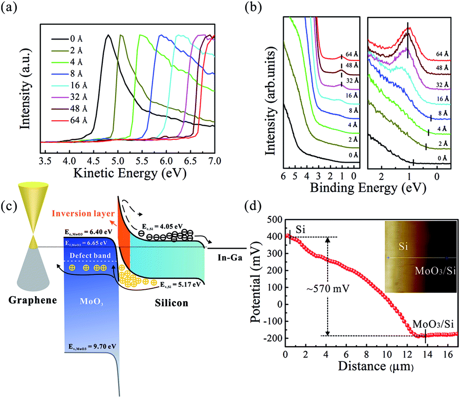 | ||
| Fig. 2 UPS spectra of bare Si and Si with varied MoO3 layer thickness: (a) secondary electron cut-off region and (b) valence band region. (c) Band alignment of the Gr/MoO3/Si heterojunction solar cell. An inversion layer was generated on Si surface due to the charge transfer between MoO3 layer and Si. (d) Cross-section line profile of the surface potential image. Inset is surface potential image of Si substrate with one half coated with MoO3 layer. | ||
In addition to UPS characterizations, the surface potential was probed using Kelvin probe force microscopy (KPFM) to visualize the effect of MoO3 on tuning the work function of Si near surface (Fig. 2d). To perform the experiment, the bare Si was partially coated with 15 nm MoO3 layer and then the scan was conducted at the border region of Si and MoO3 coated Si. Inset in Fig. 2d shows the surface potential image. The border can be easily distinguished according to the difference of colors. A lower surface potential means the high work function property by using the following equation:54,55
| Φs = Φtip − eVsp | (1) |
To gain more insight into the charge transfer between MoO3 decoration layer and the methylated silicon surface, we calculated the difference charge density (Δρ) of the methylated silicon surface after MoO3 decoration based on the first-principles calculation. Δρ is defined by the following equation: Δρ = ρMoO3/CH3–Si − ρCH3–Si − ρMoO3, where ρMoO3/CH3–Si, ρCH3–Si, and ρMoO3 represent the charge densities of the full system, the methylated silicon, and the isolated MoO3 molecule, respectively. Fig. 3a and b show the top and side views of one MoO3 molecule adsorbed on the methylated silicon surface, and the corresponding two-dimensional slice of Δρ values is plotted in Fig. 3c. The regions of electron accumulation and depletion are displayed in red and blue colors respectively in the two-dimensional slice. It is noteworthy that strong electron accumulation is present around the O atoms of MoO3 molecule, while electron depletion appears around the surface of methylated silicon. This phenomenon suggests that the adsorbed MoO3 molecule gains electrons, whereas the methylated silicon loses electrons. In addition, on the basis of Mulliken population analysis (Fig. 3d) the charge of one adsorbed MoO3 is 0.39e, indicating that a fractional positive charge of 0.39e is injected into the methylated silicon, as proved in the experiment.
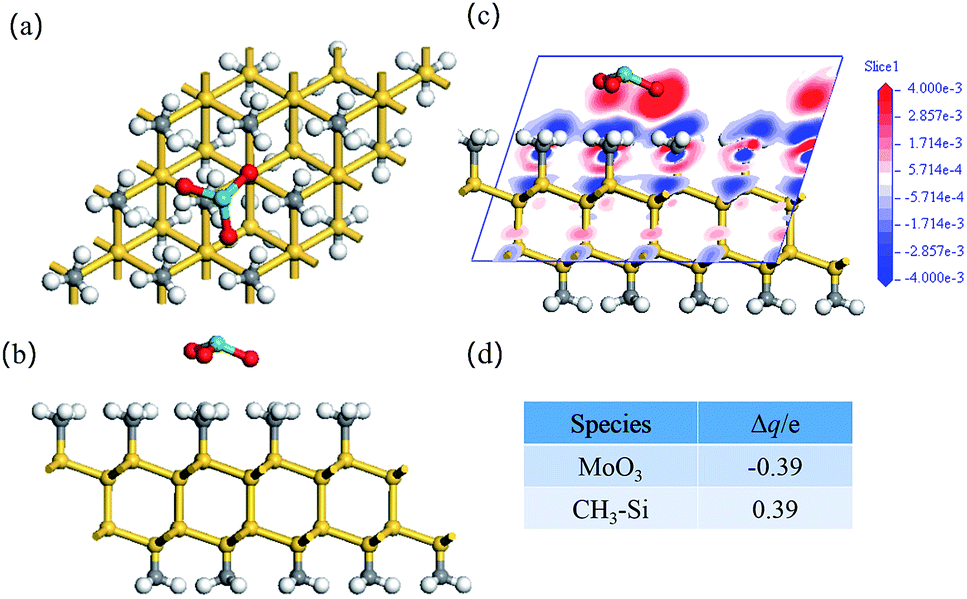 | ||
| Fig. 3 (a) Top and (b) side views of one MoO3 molecule adsorption on the methylated silicon surface. (c) Two dimensional slice contour plots of the difference charge density for the MoO3 molecule adsorbed on the methylated silicon surface. The red area represents electron accumulation, while the blue area represents electron depletion (hole accumulation). The unit of the numbers given in the legend at the right is e Å−3. (d) The Mulliken charge of MoO3 molecule and methylated silicon for the MoO3 absorption on the methylated silicon. | ||
Characterization of minority carrier lifetime was carried out to verify the reduced surface recombination due to the enhanced effective barrier height for the Gr/MoO3/Si heterojunction. The minority carrier lifetime is a visual evidence of the recombination rate of the minority carriers; longer minority carrier lifetime means lower recombination rate and thus is much desirable for high-efficiency solar cells. The minority carrier lifetime can be expressed with the following equation:
 | (2) |
 | (3) |
 | ||
Fig. 4 (a) Schematic illustration of the sample with half part coated with MoO3 decoration layer for minority carrier lifetime measurement. (b) Spatial mapping of the minority carrier lifetime of the sample. (c) Dark current density versus voltage curves of the devices with and without 15 nm MoO3 decoration layer. Inset shows the corresponding ln![[thin space (1/6-em)]](https://www.rsc.org/images/entities/char_2009.gif) J–V curves for evaluating the ideality factor. J–V curves for evaluating the ideality factor. | ||
Hole current density distribution near the junctions of the devices was simulated by Silvaco TCAD to understand how the surface reversion layer impacts the device performance. Fig. 5a and b show the device structures without and with a surface p-type inversion layer, respectively, adopted in the simulation. The device model consists of n-Si substrate, SiO2 window layer, and the transparent conductive electrode. To simplify the simulation process, the Si substrate was identified as two dimensional rectangle with size of 20 μm × 5 μm, respectively, along X axis and Y axis. The near surface inversion layer was produced via diffusion of boron atoms to the phosphorus doped n-Si substrate. Fig. 5c and d display the corresponding hole current density distribution for the devices without and with inversion layer, respectively. Compared to the device without surface inversion layer, there is an obvious improvement of the hole current density for the device with surface inversion layer from the color map difference, indicating that the collection rate of holes is effectively enhanced upon the generation of surface inversion layer. This is in well accordance with the prolonged minority carrier time mentioned above. As a result of reduced surface recombination, the Voc has remarkable increased from ∼0.13 V for the device without inversion layer to ∼0.17 V for the device with inversion layer (Fig. 5e). In contrast, the Jsc shows little enhancement. These results are also consistent with the measurement results for realistic devices in Fig. 1b.
 | ||
| Fig. 5 (a) and (b) show the schematic illustrations of the devices without and with a surface inversion layer, respectively. (c) and (d) show hole current density distribution at Y direction of the devices without and with an inversion layer, respectively. (e) Simulated J–V characteristics of the devices without and with inversion layer under AM 1.5G light illumination, respectively. | ||
Although the introduction of a MoO3 decoration layer has greatly enhanced the performance of Gr/MoO3/Si heterojunction solar cells, the device efficiency is still hindered by the relatively low conductivity of graphene and large light waste caused by high light reflection of planar Si. To further boost the device efficiency, both chemical doping on graphene and antireflection coating on the device were performed. After HNO3 doping, Fig. 6a, the PCE of the device increases from 8.18% to 10.14%, along with an obvious increase in FF from 0.58 to 0.71. This could be ascribed to the improved conductivity of graphene upon HNO3 doping.57 Moreover, by applying a PMMA antireflection layer with optimized thickness of 100 nm (Fig. S3†), the Jsc is greatly enhanced from 24.4 to 30.7 mA cm−2, giving rise to a high PCE of 12.2%. The effect of the antireflection coating can be clearly seen from the inset in Fig. 6a; the device with 100 nm PMMA coating layer (the right one) shows a darker color, indicating less light reflection and enhanced light absorption of the device. Fig. 6b depicts the correspondent EQE spectra of the device before/after HNO3 doping and with PMMA antireflection coating. It is observed that the HNO3 doping has little effect on improving the EQE value, while the PMMA antireflection coating can lead to ∼20% increase of the EQE value. The Jsc calculated by integrating the EQE curve is 31.4 mA cm−2 for the PMMA coated device, which is consistent with that obtained from the J–V curve.
 | ||
| Fig. 6 (a) Photovoltaic characteristics of the device with 15 nm MoO3 decoration layer before and after HNO3 doping. 100 nm PMMA was spin-coated onto the device surface as an antireflection layer. Inset shows the photograph of the devices without and with PMMA antireflection coating. The 100 nm PMMA-coated device is much darker than the device without coating. (b) EQE spectra of the devices with PMMA antireflection coating and graphene doping. The device without PMMA coating was also measured before/after HNO3 doping for comparison. | ||
4. Conclusions
In summary, we demonstrated a new strategy to introduce a surface inversion layer into Gr/Si heterojunction solar cell by SCTD method using transition metal oxide of MoO3 as surface dopant. Due to the high work function of MoO3 decoration layer, spontaneous hole transfer will happen at the MoO3/Si interface, leading to the generation of a p-type inversion layer on n-Si surface. The surface energy band bending, along with the increase of built-in potential at junction interface, greatly enhanced the separation/transport of photo-generated carriers and suppressed the carrier recombination at interface as well. In situ UPS, minority carrier lifetime, surface potential measurements as well as analog calculations had been conducted to verify the surface charge transfer and the formation of a surface inversion layer. A high PCE of 12.2% was eventually obtained by further combining graphene doping and PMMA antireflection coating. Given the high efficiency and simple fabrication process, the SCTD method opens up the great opportunities for high-efficiency Gr/Si heterojunction solar cells.Acknowledgements
This work was supported by the National Basic Research Program of China (No. 2013CB933500), the Major Research Plan of the National Natural Science Foundation of China (No. 91333208), the National Natural Science Foundation of China (No. 61422403, 51672108, 51622306, 21673151, 51401138, 11550110176), Qing Lan Project, and a Project Funded by the Priority Academic Program Development of Jiangsu Higher Education Institutions. We also thank the Shanghai Institute of Technical Physics (SITP) for software support.Notes and references
- T. Warabisako, T. Uematsu, S. Muramatsu, K. Tsuitsu, H. Ohtsuka, Y. Nagata and M. Sakamoto, Sol. Energy Mater. Sol. Cells, 1997, 48, 137–143 CrossRef CAS.
- G. F. Fan, H. W. Zhu, K. L. Wang, J. Q. Wei, X. M. Li, Q. K. Shu, N. Guo and D. H. Wu, ACS Appl. Mater. Interfaces, 2011, 3, 721–725 CAS.
- C. Xie, P. Lv, B. Nie, J. S. Jie, X. W. Zhang, Z. Wang, P. Jiang, Z. Z. Hu, L. B. Luo, Z. F. Zhu, L. Wang and C. Y. Wu, Appl. Phys. Lett., 2011, 99, 133113 CrossRef.
- T. T. Feng, D. Xie, Y. X. Lin, Y. Y. Zang, T. L. Ren, R. Song, H. M. Zhao, H. Tian, X. Li, H. W. Zhu and L. T. Liu, Appl. Phys. Lett., 2011, 99, 233505 CrossRef.
- X. Z. Zhang, C. Xie, J. S. Jie, X. W. Zhang, Y. M. Wu and W. J. Zhang, J. Mater. Chem. A, 2013, 1, 6593–6601 CAS.
- C. Xie, X. J. Zhang, K. Q. Ruan, Z. B. Shao, S. S. Dhaliwal, L. Wang, Q. Zhang, X. W. Zhang and J. S. Jie, J. Mater. Chem. A, 2013, 1, 15348–15354 CAS.
- E. Z. Shi, H. B. Li, L. Yang, L. H. Zhang, Z. Li, P. X. Li, Y. Y. Shang, S. T. Wu, X. M. Li, J. Q. Wei, K. L. Wang, H. W. Zhu, D. H. Wu, Y. Fang and A. Y. Cao, Nano Lett., 2013, 13, 1776–1781 CrossRef CAS PubMed.
- L. B. Luo, C. Xie, X. H. Wang, Y. Q. Yu, C. Y. Wu, H. Hu, K. Y. Zhou, X. W. Zhang and J. S. Jie, Nano Energy, 2014, 9, 112–120 CrossRef CAS.
- C. Xie, X. Z. Zhang, Y. M. Wu, X. J. Zhang, X. W. Zhang, Y. Wang, W. J. Zhang, P. Gao, Y. Y. Han and J. S. Jie, J. Mater. Chem. A, 2013, 1, 8567–8574 CAS.
- K. J. Jiao, X. L. Wang, Y. Wang and Y. F. Chen, J. Mater. Chem. C, 2014, 2, 7715–7721 RSC.
- L. F. Yang, X. G. Yu, X. S. Xu, H. Z. Chen and D. R. Yang, J. Mater. Chem. A, 2014, 2, 16877–16883 CAS.
- Y. Song, X. M. Li, C. Mackin, X. Zhang, W. J. Fang, T. Palacios, H. W. Zhu and J. Kong, Nano Lett., 2015, 15, 2104–2110 CrossRef CAS PubMed.
- Y. Tsuboi, F. J. Wang, D. Kozawa, K. Funahashi, S. Mouri, Y. Miyauchi, T. Takenobu and K. Matsuda, Nanoscale, 2015, 7, 14476–14482 RSC.
- D. K. Xu, X. G. Yu, L. J. Zuo and D. R. Yang, RSC Adv., 2015, 5, 46480–46484 RSC.
- Y. M. Wu, X. Z. Zhang, J. S. Jie, C. Xie, X. W. Zhang, B. Q. Sun, Y. Wang and P. Gao, J. Phys. Chem. C, 2013, 117, 11968–11976 CAS.
- X. C. Miao, S. Tongay, M. K. Petterson, K. Berke, A. G. Rinzler, B. R. Appleton and A. F. Hebard, Nano Lett., 2012, 12, 2745–2750 CrossRef CAS PubMed.
- P. H. Ho, Y. T. Liou, C. H. Chuang, S. W. Lin, C. Y. Tseng, D. Y. Wang, C. C. Chen, W. Y. Hung, C. Y. Wen and C. W. Chen, Adv. Mater., 2015, 27, 1724–1729 CrossRef CAS PubMed.
- X. Liu, X. W. Zhang, Z. G. Yin, J. H. Meng, H. L. Gao, L. Q. Zhang, Y. J. Zhao and H. L. Wang, Appl. Phys. Lett., 2014, 105, 183901 CrossRef.
- L. F. Yang, X. G. Yu, W. D. Hu, X. L. Wu, Y. Zhao and D. R. Yang, ACS Appl. Mater. Interfaces, 2015, 7, 4135–4141 CAS.
- X. G. Yu, L. F. Yang, Q. M. Lv, M. S. Xu, H. Z. Chen and D. R. Yang, Nanoscale, 2015, 7, 7072–7077 RSC.
- P. H. Ho, W. C. Lee, Y. T. Liou, Y. P. Chiu, Y. S. Shih, C. C. Chen, P. Y. Su, M. K. Li, H. L. Chen, C. T. Liang and C. W. Chen, Energy Environ. Sci., 2015, 8, 2085–2092 CAS.
- X. M. Li, H. W. Zhu, K. L. Wang, A. Y. Cao, J. Q. Wei, C. Y. Li, Y. Jia, Z. Li, X. Li and D. H. Wu, Adv. Mater., 2010, 22, 2743–2748 CrossRef CAS PubMed.
- R. R. Nair, P. Blake, A. N. Grigorenko, K. S. Novoselov, T. J. Booth, T. Stauber, N. M. Peres and A. K. Geim, Science, 2008, 320, 1308 CrossRef CAS PubMed.
- P. A. George, J. Strait, J. Dawlaty, S. Shivaraman, M. Chandrashekhar, F. Rana and M. G. Spencer, Nano Lett., 2008, 8, 4248–4251 CrossRef CAS PubMed.
- A. Wang, J. Zhao and M. A. Green, Appl. Phys. Lett., 1990, 57, 602–604 CrossRef CAS.
- J. H. Zhao, A. H. Wang, M. A. Green and F. Ferrazza, Appl. Phys. Lett., 1998, 73, 1991–1993 CrossRef CAS.
- Y. W. Kuang, Y. S. Liu, Y. L. Ma, X. K. Hong, X. F. Yang and J. F. Feng, J. Nanoelectron. Optoelectron., 2015, 10, 611–615 CrossRef CAS.
- Y. W. Kuang, D. B. Zhang, Y. L. Ma, Y. S. Liu, Z. G. Shao, X. K. Hong, X. F. Yang and J. F. Feng, Opt. Quantum Electron., 2016, 48, 199 CrossRef.
- H. D. Um, N. Kim, K. Lee, I. Hwang, J. H. Seo and K. Seo, Nano Lett., 2016, 16, 981–987 CrossRef CAS PubMed.
- C. S. Guo, L. B. Luo, G. D. Yuan, X. B. Yang, R. Q. Zhang, W. J. Zhang and S. T. Lee, Angew. Chem., Int. Ed., 2009, 48, 9896–9900 CrossRef CAS PubMed.
- G. D. Yuan, Y. B. Zhou, C. S. Guo, W. J. Zhang, Y. B. Tang, Y. Q. Li, Z. H. Chen, Z. B. He, X. J. Zhang and P. F. Wang, ACS Nano, 2010, 4, 3045–3052 CrossRef CAS PubMed.
- P. Strobel, M. Riedel, J. Ristein and L. Ley, Nature, 2004, 430, 439–441 CrossRef CAS PubMed.
- A. Javey, R. Tu, D. B. Farmer, J. Guo, R. G. Gordon and H. J. Dai, Nano Lett., 2005, 5, 345–348 CrossRef CAS PubMed.
- K. K. Kim, J. J. Bae, H. K. Park, S. M. Kim, H. Z. Geng, K. A. Park, H. J. Shin, S. M. Yoon, A. Benayad and J. Y. Choi, J. Am. Chem. Soc., 2008, 130, 12757–12761 CrossRef CAS PubMed.
- A. C. Crowther, A. Ghassaei, N. Jung and L. E. Brus, ACS Nano, 2012, 6, 1865–1875 CrossRef CAS PubMed.
- H. M. Li, D. Lee, D. Qu, X. Liu, J. Ryu, A. Seabaugh and W. J. Yoo, Nat. Commun., 2015, 6, 6564 CrossRef CAS PubMed.
- D. Xiang, C. Han, J. Wu, S. Zhong, Y. Y. Liu, J. D. Lin, X. A. Zhang, W. P. Hu, B. Özyilmaz and A. C. Neto, Nat. Commun., 2015, 6, 6485 CrossRef CAS PubMed.
- J. S. Jie, W. J. Zhang, K. Q. Peng, G. D. Yuan, C. S. Lee and S. T. Lee, Adv. Funct. Mater., 2008, 18, 3251–3257 CrossRef CAS.
- G. D. Yuan, T. W. Ng, Y. B. Zhou, F. Wang, W. J. Zhang, Y. B. Tang, H. B. Wang, L. B. Luo, P. F. Wang, I. Bello, C. S. Lee and S. T. Lee, Appl. Phys. Lett., 2010, 97, 153126 CrossRef.
- F. Z. Li, L. B. Luo, Q. D. Yang, D. Wu, C. Xie, B. Nie, J. S. Jie, C. Y. Wu, L. Wang and S. H. Yu, Adv. Energy Mater., 2013, 3, 579–583 CrossRef CAS.
- Z. B. Shao, J. S. Jie, Z. Sun, F. F. Xia, Y. M. Wang, X. H. Zhang, K. Ding and S. T. Lee, Nano Lett., 2015, 15, 3590–3596 CrossRef CAS PubMed.
- X. S. Li, W. W. Cai, J. An, S. Kim, J. Nah, D. X. Yang, R. Piner, A. Velamakanni, I. Jung, E. Tutuc, S. K. Banerjee, L. Colombo and R. S. Ruoff, Science, 2009, 324, 1312–1314 CrossRef CAS PubMed.
- Y. Wang, S. W. Tong, X. F. Xu, B. Ozyilmaz and K. P. Loh, Adv. Mater., 2011, 23, 1514–1518 CrossRef CAS PubMed.
- E. J. Nemanick, P. T. Hurley, B. S. Brunschwig and N. S. Lewis, J. Phys. Chem. B, 2006, 110, 14800–14808 CrossRef CAS PubMed.
- M. C. Lu, R. B. Wang, A. Yang and S. Duhm, J. Phys.: Condens. Matter, 2016, 28, 094005 CrossRef PubMed.
- S. J. Clark, M. D. Segall, C. J. Pickard, P. J. Hasnip, M. I. J. Probert, K. Refson and M. C. Payne, Z. Kristallogr., 2005, 220, 567–570 CAS.
- J. P. Perdew and Y. Wang, Phys. Rev. B: Condens. Matter Mater. Phys., 1992, 45, 13244–13249 CrossRef.
- J. P. Perdew, K. Burke and M. Ernzerhof, Phys. Rev. Lett., 1996, 77, 3865–3868 CrossRef CAS PubMed.
- H. J. Monkhorst and J. D. Pack, Phys. Rev. B: Solid State, 1976, 13, 5188–5192 CrossRef.
- R. Y. Liu, S. T. Lee and B. Q. Sun, Adv. Mater., 2014, 26, 6007 CrossRef CAS PubMed.
- M. Kröger, S. Hamwi, J. Meyer, T. Riedl, W. Kowalsky and A. Kahn, Appl. Phys. Lett., 2009, 95, 123301 CrossRef.
- J. P. Yang, Y. Xiao, Y. H. Deng, S. Duhm, N. Ueno, S. T. Lee, Y. Q. Li and J. X. Tang, Adv. Funct. Mater., 2012, 22, 600–608 CrossRef CAS.
- C. Battaglia, X. T. Yin, M. Zheng, I. D. Sharp, T. Chen, S. McDonnell, A. Azcatl, C. Carraro, B. W. Ma, R. Maboudian, R. M. Wallace and A. Javey, Nano Lett., 2014, 14, 967–971 CrossRef CAS PubMed.
- X. J. Shen, Y. W. Zhu, T. Song, S. T. Lee and B. Q. Sun, Appl. Phys. Lett., 2013, 103, 013504 CrossRef.
- Y. F. Zhang, W. Cui, Y. W. Zhu, F. S. Zu, L. S. Liao, S. T. Lee and B. Q. Sun, Energy Environ. Sci., 2015, 8, 297–302 CAS.
- S. M. Sze, Physics of Semiconductor Devices, Wiley, New York, 1969, p. 643 Search PubMed.
- H. T. Liu, Y. Q. Liu and D. B. Zhu, J. Mater. Chem., 2011, 21, 3335–3345 RSC.
Footnote |
| † Electronic supplementary information (ESI) available. See DOI: 10.1039/c6ta07100g |
| This journal is © The Royal Society of Chemistry 2017 |