
 Open Access Article
 This Open Access Article is licensed under a
 Creative Commons Attribution 3.0 Unported Licence
Plasmonic nanoparticle-semiconductor composites for efficient solar water splitting
M.
Valenti
*a,
M. P.
Jonsson
 b,
G.
Biskos
cd,
A.
Schmidt-Ott
a and
W. A.
Smith
*a
b,
G.
Biskos
cd,
A.
Schmidt-Ott
a and
W. A.
Smith
*a
aMaterials for Energy Conversion and Storage (MECS), Department of Chemical Engineering, Faculty of Applied Sciences, Delft University of Technology, Delft 2628-BL, The Netherlands. E-mail: m.valenti@tudelft.nl; w.smith@tudelft.nl
bLaboratory of Organic Electronics, Department of Science and Technology, Campus Norrköping, Linköping University, SE-60174 Norrköping, Sweden
cFaculty of Civil Engineering and Geosciences, Delft University of Technology, Delft 2628-CN, The Netherlands
dEnergy Environment and Water Research Center, The Cyprus Institute, Nicosia 2121, Cyprus
First published on 5th October 2016
Abstract
Photoelectrochemical (PEC) water splitting is a promising technology that uses light absorbing semiconductors to convert solar energy directly into a chemical fuel (i.e., hydrogen). PEC water splitting has the potential to become a key technology in achieving a sustainable society, if high solar to fuel energy conversion efficiencies are obtained with earth abundant materials. This review article discusses recent developments and discoveries in the mechanisms by which the localized surface plasmon resonance (LSPR) in metallic nanoparticles can increase or complement a neighbouring semiconductor in light absorption for catalytic water splitting applications. These mechanisms can mitigate the intrinsic optical limitations of semiconductors (e.g., metal oxides) for efficient solar water splitting. We identify four types of enhancement mechanisms in the recent literature: (i) light scattering, (ii) light concentration, (iii) hot electron injection (HEI), and (iv) plasmon-induced resonance energy transfer (PIRET). (i) Light scattering and (ii) light concentration are light trapping mechanisms that can increase the absorption of light with energies above the semiconductor optical band-edge. These two mechanisms are ideal to enhance the absorption of promising semiconductors with narrow bandgap energies that suffer from limited absorption coefficients and bulk charge recombination. On the other hand, (iii) HEI and the recently discovered (iv) PIRET are mechanisms that can enhance the absorption also below the semiconductor optical band-edge. Therefore, HEI and PIRET have the potential to extend the light utilization to visible and near-infrared wavelengths of semiconductors with excellent electrochemical properties, but with large bandgap energies. New techniques and theories that have been developed to elucidate the above mentioned plasmonic mechanisms are presented and discussed for their application in metal oxide photoelectrodes. Finally, other plasmonic and non-plasmonic effects that do not increase the device absorption, but affect the electrochemical properties of the semiconductor (e.g., charge carrier transport) are also discussed, since a complete understanding of these phenomena is fundamental for the design of an efficient plasmonic NP-semiconductor water splitting device.
 M. Valenti | Marco Valenti is a Ph.D. student supervised by Prof. Dr Andreas Schmidt-Ott at Delft University of Technology, The Netherlands. His research is focused on developing efficient materials for solar-to-fuel energy conversion. His main interests are twofold: (i) improving the opto-electronic properties of water splitting semiconductor photoelectrodes by plasmonic nanoparticle functionalization, and (ii) studying the activity/selectivity in the electrochemical CO2 reduction over noble metal alloy nanoparticles. |
 M. P. Jonsson | Dr Magnus Jonsson is an assistant professor at the Laboratory of Organic Electronics at Linköping University in Sweden. Before that he was a postdoctoral Wenner-Gren Fellow at the Kavli Institute of Nanoscience at Delft University of Technology, the Netherlands. Dr Jonsson's research explores nanooptical phenomena for energy harvesting and bio applications. Related topics of interest include optoelectronic paper and nanofabrication. Important contributions include plasmonic nanopores for single-molecule detection and nanoplasmonic biosensors. He is the recipient of several grants and awards, including an Ingvar Carlsson Award from the Swedish Foundation for Strategic Research and the Elsevier Biosensors and Bioelectronics Award 2010. |
 G. Biskos | Dr George Biskos is an Associate Professor at the Cyprus Institute and at the Delft University of Technology. Previously he has been a faculty member at the University of the Aegean and a Research Associate at Harvard University. He holds a PhD in Engineering from Cambridge University, and an MSc in Environmental Engineering from Imperial College, UK. His research interests are in the broader area of aerosol science and technology, ranging from instrumentation development for measuring airborne particles, to atmospheric aerosols and aerosol based nanotechnology. |
 A. Schmidt-Ott | Prof. Dr Andreas Schmidt-Ott received his Ph.D. from ETH Zurich, Switzerland. There, he worked at the Atmospheric Physics Department and later at the Solid State Physics Laboratory. He spent a term at the Chemical Engineering Department of the University of California, Los Angeles as a Visiting Assistant Professor before joining Duisburg University, Germany. Here, he was first Assistant Professor at the Faculty of Electrical Engineering and then became professor in the Mechanical Engineering Department. Since 2001 he is a Professor of Particle Technology in the Materials for Energy Conversion and Storage section at Delft University of Technology, Netherlands. He received the Smoluchowski Award in 1989. |
 W. A. Smith | Dr Wilson A. Smith is an Associate Professor in the Department of Chemical Engineering at Delft University of Technology. He received his BSc (2005) and PhD (2010) in Physics before moving to the Universite Pierre et Marie Curie/Sorbonne in Paris, France to begin studying chemical engineering. Since 2012, he has lead a research group in Delft that focuses on fundamental processes related to photo electrochemical water splitting, electrocatalytic water oxidation, and CO2 reduction catalysis using inorganic nanostructured materials. His group uses many in situ electrochemical characterization tools to examine the electrode/electrolyte interface in these systems, with the aim to develop stable, selective, and efficient catalysts for the sustainable conversion and storage of renewable energy. |
1. Introduction
Photoelectrochemical (PEC) water splitting offers a sustainable and clean way to store solar energy in the form of a chemical fuel, i.e. hydrogen. This process has benefited from over 40 years of research,1,2 and many advances have been made with respect to the materials used today,3,4 while our overall understanding of the photo physical–chemical processes involved in the overall reaction has improved significantly. The main challenges that remain for PEC water splitting are finding materials that can simultaneously harvest solar irradiation, create and separate electronic charges (electrons and holes), and drive the water reduction and oxidation reactions. Furthermore, in order to bring this technology to a practical level, the entire process must be accomplished by inexpensive earth abundant materials that are stable in an electrochemical environment.The most successful materials used to drive the solar water splitting reaction are semiconductor photoelectrodes, where metal oxides like TiO2,1 WO3,5,6 Fe2O3,7–9 Cu2O,10,11 and BiVO4 (ref. 12–15) have received the most attention. These materials have been extensively studied and have emerged as promising candidates for practical applications as they are made from earth abundant materials that are generally stable in aqueous environments. However, metal oxide photoelectrodes often have less than ideal opto-electronic and catalytic properties, exhibited by low absorption coefficients, large band gap energies, short charge carrier diffusion lengths and life-times, and sluggish reaction kinetics at their surface.3 Therefore, significant efforts have been devoted to functionalize metal oxide semiconductors photoelectrodes to improve their optical, electronic, and catalytic properties.16–18
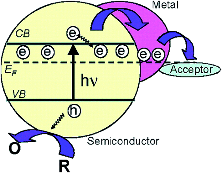
One promising solution is to decorate semiconductors with plasmonic nanoparticles (NPs).19–21 These metallic NPs can increase the absorption of thin film semiconductor photoelectrodes (with low absorption coefficients) by either confining or scattering the light into the semiconductor (i.e., light trapping).20–22 In addition, plasmonic NPs can absorb visible light with lower energies (i.e. higher wavelengths) than the semiconductor band gap and subsequently transfer the absorbed energy to the semiconductor in the form of “hot electrons” (electrons with energies higher than the metal Fermi level)23,24 or in a dipole–dipole interaction,25 effectively extending the semiconductor absorption range. At the same time, the plasmonic NPs can significantly improve the electronic26 and catalytic27 properties of semiconductors when the NPs are placed at the semiconductor–electrolyte interface. All these possibilities have resulted in the synthesis and photoelectrochemical testing of many different plasmonic NP/semiconductor composites, to elucidate the phenomena and exploit their use for solar driven water splitting.18,25,28–31
Recent reviews19,32,33 on plasmonic photocatalysis have mainly focused on plasmonic mechanisms that enhance the semiconductor absorption. However, less emphasis has been given to plasmonic and non-plasmonic NP effects on the charge transport properties and energetics of the semiconductor. In this review, we discuss how plasmonic NP size, shape, and composition affect the optical properties, charge transport and energetics of semiconductor photoelectrodes for PEC water splitting. Particular emphasis is given to decoupling plasmon-induced and non-plasmon-induced effects that are generated by NP/semiconductor composites, in order to gain mechanistic insights into the structure–functionality relationship of these promising architectures to improve PEC water spitting.
2. Localized surface plasmon resonance
Light in the UV-visible wavelength range can induce collective oscillations of the valence electrons in noble metal NPs.34,35 This phenomenon is known as localized surface plasmon resonance (LSPR). The oscillating electron cloud (called localized surface plasmon) exhibits a life-time on the order of femtoseconds that is limited by different radiative and non-radiative damping processes.36 The population of surface plasmons that decays by radiative damping is converted into photons, whereas, the population that decays by non-radiative damping is converted into electron–hole pairs by interband and intraband excitations (cf.Fig. 1).36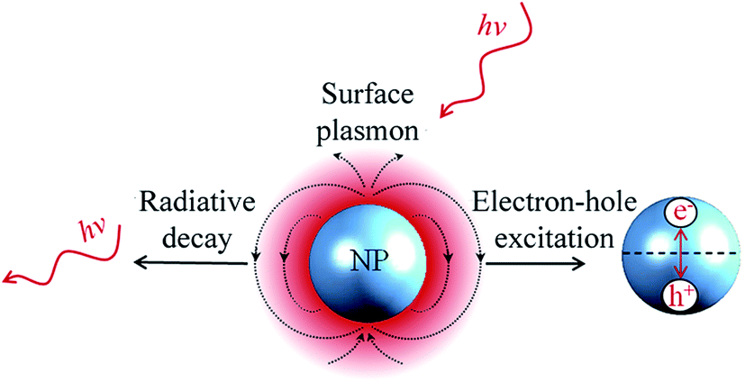 | ||
| Fig. 1 Illustration of radiative (left) and non-radiative (right) decay of the NP surface plasmon. The non-radiative decay occurs due to intraband excitation within the conduction band. | ||
2.1. Absorption and scattering cross sections
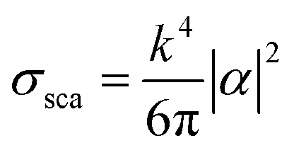
Metal NPs whose surface plasmons mainly decay through non-radiative processes are called light absorbing NPs, since the irradiating energy (e.g., solar radiation) is absorbed by the NPs and subsequently transferred to their surroundings (e.g., by releasing heat). For applications where non-radiative processes are desired, light absorbing NPs with a large absorption cross-section and a small scattering (radiative decay) cross-section are selected. In 1908, Gustav Mie derived analytical expressions for the absorption and scattering cross-sections of spherical NPs of arbitrary size.34 This theory has evolved to the generalized Mie theory that can also accurately predict the optical behaviour of particles of different shapes, such as ellipsoids and rods.37 The NP scattering cross section (σsca) and absorption cross section (σabs) for small spheres can be approximated using eqn (1)–(3). This approximation is justified by Mie theory for spherical particles in the limit ak ≪ 1 and |m|ak ≪ 1, where a is the radius of the particle, k is the wave number and m is the refractive index of the particle relative to that of the medium:38| σabs = kIm(α) | (1) |
 | (2) |
 | (3) |
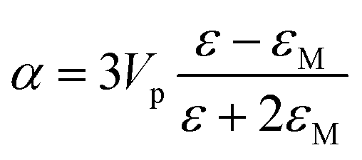
For ellipsoidal NPs, a simple expression for the polarizability along direction i = 1, 2, 3 can be obtained with the, less rigorous, electrostatic approximation (or dipole approximation) for small particles compared with the light wavelength:38
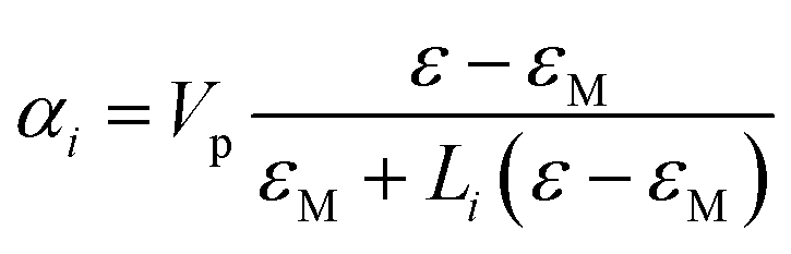 | (4) |
Eqn (1)–(4) clearly show that the absorption and scattering cross sections depend on the NP size (Vp), shape (Li) and composition (ε), along with the surrounding media (εM). Regarding size, the scattering cross section is proportional to Vp2, while the absorption cross section is proportional to Vp. For example, Fig. 2 shows that the scattering cross section of a spherical gold NP nearly vanishes when its radius is decreased from 35 nm (Fig. 2A) to 10 nm (Fig. 2B), while the absorption cross section is decreased to a lesser extent. Therefore, small NPs are used for applications where only non-radiative decays are desired.
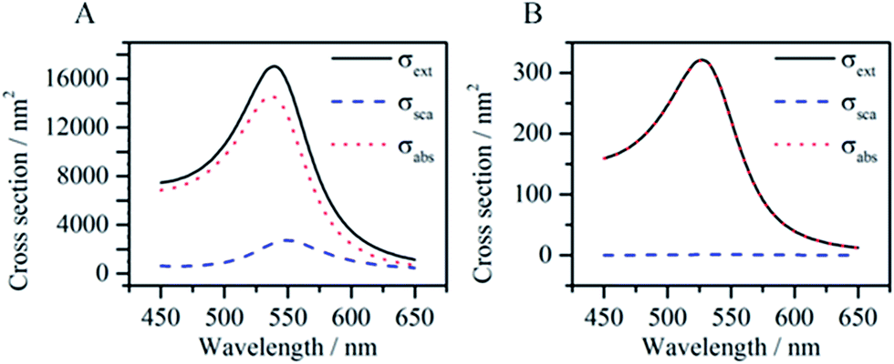 | ||
| Fig. 2 Extinction, scattering and absorption spectra of a gold NP with a radius of 35 nm (A) and a radius of 10 nm (B) calculated using Mie theory. In both cases, the refractive index of the environment is 1.33. | ||
2.2. Plasmon resonance frequency
The light frequency at which the NP extinction coefficient is the greatest is called the NP plasmon resonance frequency, and it can be tuned by changing the material composition, shape and size of the NPs as shown in Fig. 3. Fig. 3A also highlights that noble metal NPs interact significantly with light that is abundant in the solar irradiation spectrum, which makes them excellent candidates to be used in solar energy conversion devices. The NP absorption and scattering spectra are also affected by the dielectric function of the surrounding medium (cf.eqn (1)–(3)). Even though the dielectric function of the surrounding medium is determined by the application (e.g., aqueous solution for PEC water splitting), it can be partially modified by coating the NP with a thin semiconducting or insulating layer. The dielectric function and the thickness of the coating can be changed to tune the resonance frequency of the NPs.39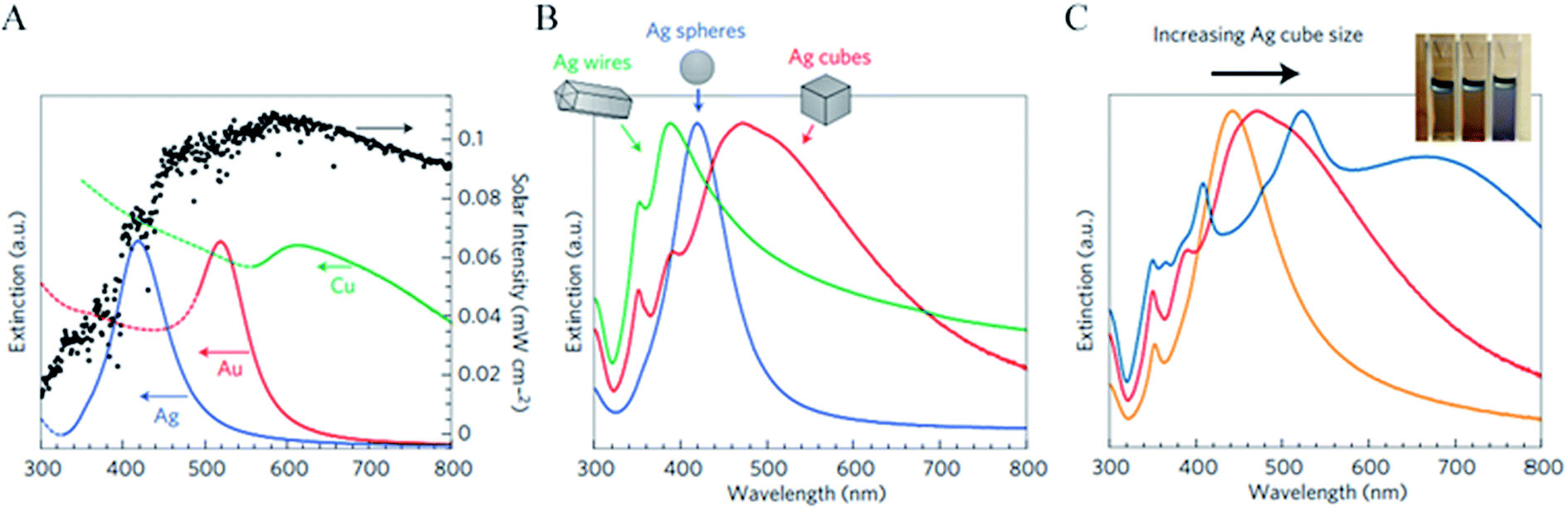 | ||
| Fig. 3 (A) Normalized extinction spectra of spherical Ag (38 ± 12 nm in diameter), Au (25 ± 5 nm) and Cu (133 ± 23 nm) particles. The intensity of solar radiation (data for air mass 1.5 solar spectrum from the National Renewable Energy Laboratory, http://rredc.nrel.gov/solar/spectra/am1.5/) is also shown, in black. Dashed portions of the metal extinction curves indicate interband transitions (that is, no surface plasmon resonance in these regions). (B) Normalized extinction spectra for Ag wire, cube and sphere nanoparticles. Wire-shaped particles are 90 ± 12 nm diameter and >30 aspect ratio, cubic particles are 79 ± 12 nm edge length and spherical particles are 38 ± 12 nm diameter. (C) Normalized extinction spectra for Ag nanocubes as a function of size (56 ± 8 nm, 79 ± 13 nm and 129 ± 7 nm edge lengths correspond to orange, red and blue spectra respectively). The inset shows a photograph of the three nanocube samples suspended in ethanol.20 Reprinted with permission from ref. 20. Copyright 2011 Macmillan publishers limited. | ||
Significant tunability of the LSPR extinction spectra has been achieved with metal NP rods and NP dimers (two closely spaced NPs), since they are characterized by two LSPR modes corresponding to excitation at different polarizations (i.e., transversal and longitudinal modes).40–42 In NP rods, the longitudinal mode can be accurately tuned by modifying the length of the rod,40 whereas, for NP dimers the longitudinal mode can be tuned by modifying the interparticle distance (cf.Fig. 4).41,43
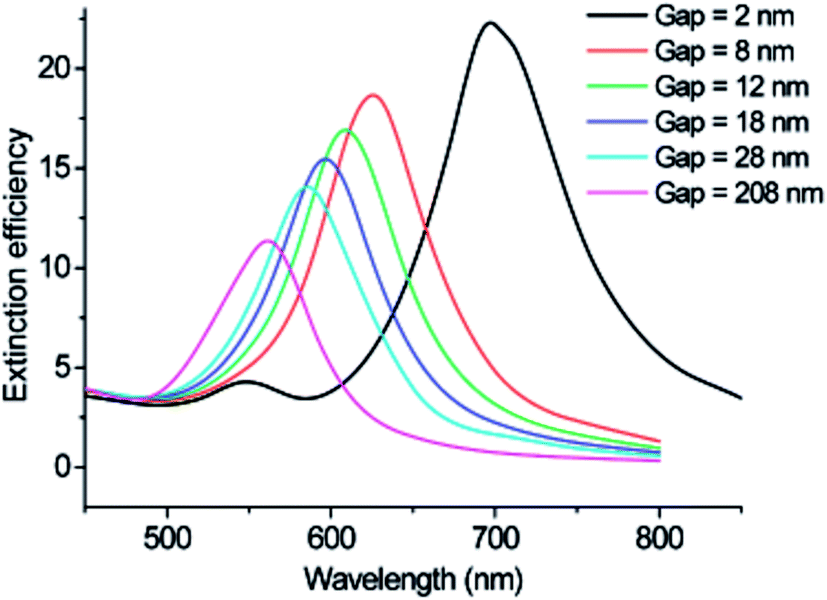 | ||
| Fig. 4 Discrete dipole approximation-simulated extinction efficiency spectra of Au nanodisc pairs for varying interparticle separation gap for incident light polarized parallel to the interparticle axis (longitudinal mode). Reprinted with permission from ref. 43. Copyright 2007 ACS. | ||
2.3. Light confinement (NP near-field)
An important characteristic of the LSPR is the highly localized electric field enhancement around the plasmonic NP. Fig. 5A shows the electric field contours of a silver NP when illuminated with light at the NP resonance frequency. It can be seen that the magnitude of the applied electric field is enhanced by ∼50 fold at the NP surface. This near-field effect plays an important role in several applications, such as waveguiding along particle chains,44 surface-enhanced Raman scattering (SERS),45 light trapping to enhance light absorption in semiconductors46 (discussed in the following section), among others. Higher field enhancements are achieved with particles having sharp edges, such as the NP rod shown in Fig. 5B. Finally, the formation of NP dimers (e.g., spherical,47 rod48 and triangular prism47,49,50 dimers) give rise to the largest field enhancements that are order of magnitudes larger than the applied field (cf.Fig. 5C).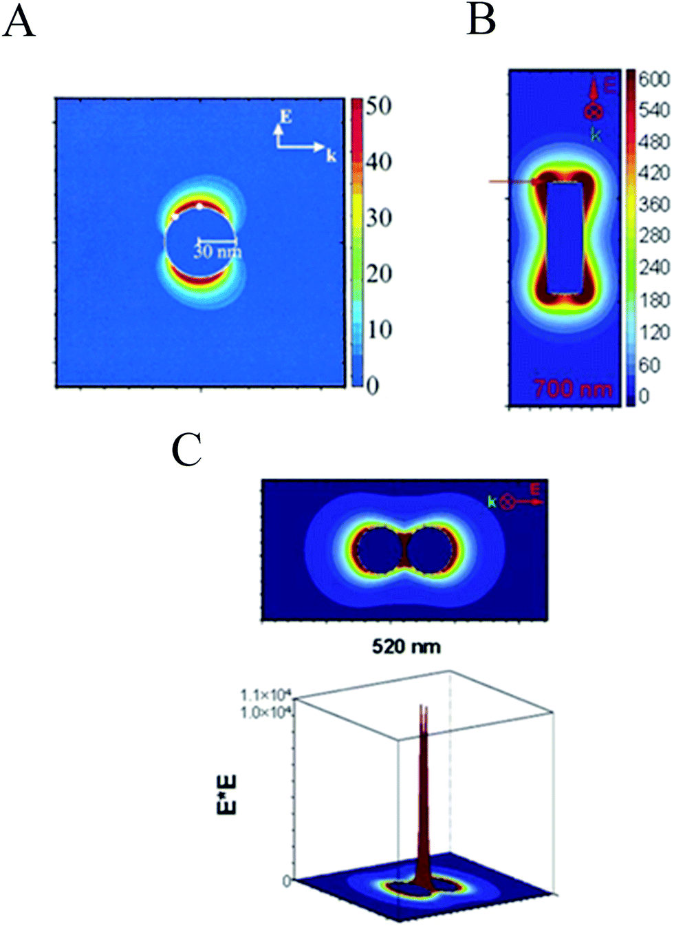 | ||
| Fig. 5 (A) Electric field enhancement contours for a Ag sphere. Reprinted in part with permission from ref. 35. Copyright 2002 ACS (B) electric field enhancement contours for a rod. Reprinted in part with permission from ref. 47. Copyright 2004 AIP (C) electric field enhancement contours external to a dimer of Ag nanoparticles separated by 2 nm, for a plane that is along the inter-particle axis and that passes midway throng the two particles. In the 3D plots, the axis perpendicular to the selected plane represents the amount of electric field enhancement around the dimer.47 Reprinted in part with permission from ref. 47. Copyright 2004 AIP. | ||
3. Plasmonic NP/semiconductor composites
3.1. Harvesting the surface plasmon's energy to drive the water splitting half reactions on semiconductors
For a NP in contact with a semiconductor, (part of) the surface plasmon's energy can be extracted for both radiative damping and non-radiative damping (Fig. 6A and B). The surface plasmon energy can be transferred from the NP to the semiconductor and then further converted to chemical energy, for example, to drive the water splitting reactions. This energy transfer is possible through four different mechanisms that form the core of this review. These are (i) light scattering (radiative decay, Fig. 6A), (ii) hot electron injection (HEI, Fig. 6B), (iii) light concentration (Fig. 6C) and (iv) plasmon-induced resonance energy transfer (PIRET, Fig. 6D). Light scattering by radiative decay (i) can enhance the effective optical path length in the semiconductor. This leads to corresponding enhanced absorption and generation of charge carriers that can drive the water splitting half reactions (Fig. 6A).22 Instead, when the surface plasmon decays by exciting an electron–hole pair within the NP (non-radiative decay, Fig. 6B) (ii), hot electrons can be transferred to the conduction band of the semiconductor. Once the hot electron and hole are separated, they can carry out the corresponding water splitting half reactions.23 In the third (light concentration) and fourth (PIRET) mechanisms, the highly localized electric field enhancement (i.e., near-field) around the plasmonic NP induces interband excitations in a neighbouring semiconductor (Fig. 6C and D).51,52 In both mechanisms, the plasmon energy transfer to the semiconductor is mediated by coupling between photons, plasmons and excitons (electron–hole pairs) in the NP near-field. Unlike direct light excitation, the near-field can induce excitations not only above, but also below the optical band gap edge (OBGE) of the semiconductor. This review distinguishes between near-field effects acting above the OBGE (i.e., light concentration mechanism) and below the OBGE (i.e., PIRET), since they have different implications (cf. Section 4.2.2). In the light concentration mechanism (iii) the NPs act as optical antennas that localize the incident electromagnetic field in the neighbouring semiconductor, increasing the electron–hole generation rate in the semiconductor (Fig. 6C).31,46,53 In PIRET, the near-field energy is transferred non-radiatively to the semiconductor through strong dipole–dipole coupling with band edge states that are optically inaccessible (Fig. 6D).25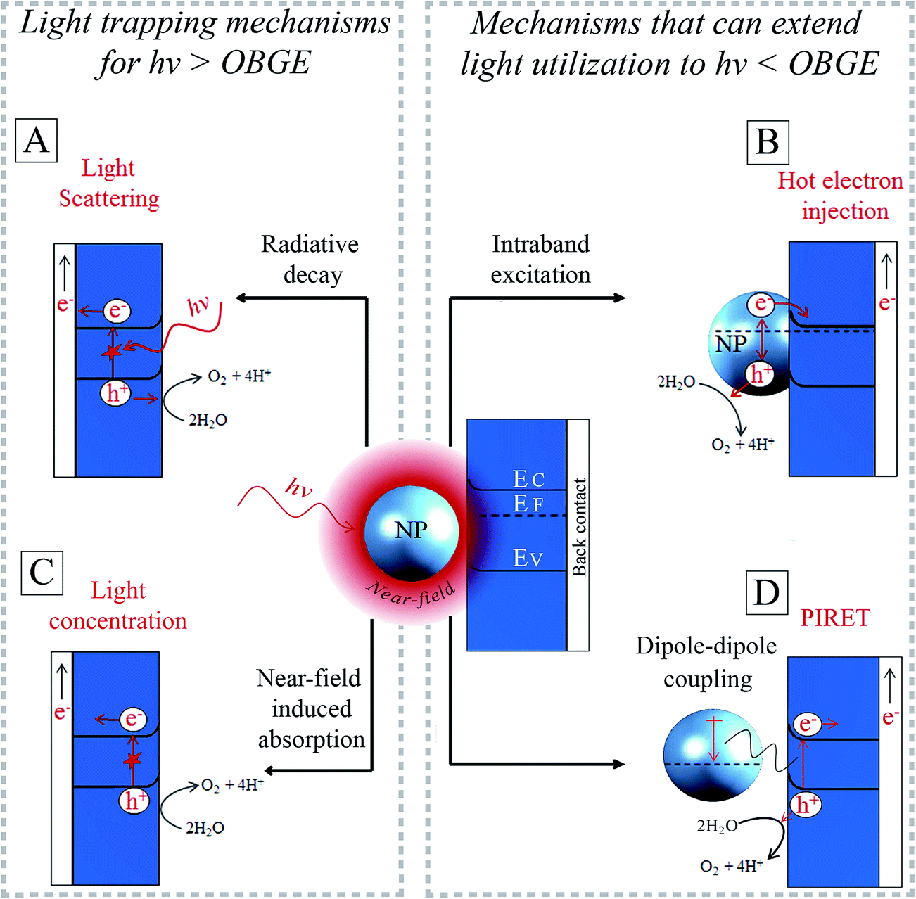 | ||
| Fig. 6 Illustration of four energy transfer mechanisms from a plasmonic NP to an n-type semiconductor to drive water oxidation: (A) light scattering, (B) hot electron injection, (C) light concentration and (D) plasmon-induced resonance energy transfer (PIRET). OBGE denotes the optical band gap edge of the semiconductor. EC, EF, EV are the conduction band, Fermi and valence band energies, respectively. | ||
Because the light scattering (i) and the light concentration (iii) mechanisms both effectively guide and/or localize the incoming photons, these mechanisms are referred to as light trapping or photonic effects (Fig. 6A and C).54 While the light trapping mechanisms are only effective with incident photon energies above the OBGE, HEI and PIRET can extend the light utilization to photon energies below the OBGE (Fig. 6B and D). These four energy transfer mechanisms (i.e., light scattering, HEI, light concentration and PIRET), allow decorating plasmonic NPs to enhance or complement the insufficient light absorption of bare semiconductors and, therefore, improve the overall performance of conventional water splitting semiconductor devices.
New strategies and materials have been developed in recent years to efficiently exploit the surface plasmon energy in plasmonic NP/metal oxide photoelectrodes in order to mitigate the optical limitations of bare semiconductor metal oxide photoelectrodes (i.e., large bandgap energies and low absorption coefficients).18,19,25–27,54–56 Recent key publications that have elucidated the roles of each mechanism for the water splitting performance of NP-metal oxide photoelectrodes are reviewed in Section 4 along with a more detailed description of the corresponding mechanisms.
3.2. Electrochemical effects
The plasmonic mechanisms described above are summarized in Fig. 7 together with other metal NP mechanisms, either plasmonic or non-plasmonic, that enhance the performance of semiconductor photoelectrodes. HEI, PIRET and light trapping are the mechanisms by which plasmonic NPs can increase the light absorption in the semiconductor. In addition, decorating plasmonic NPs on semiconductors can also cause other important electrochemical effects that can enhance the water splitting performance of the semiconductor. In turn, these electrochemical effects can be divided into those that affect (i) the semiconductor's charge transport, and (ii) its electronic band energetics (cf.Fig. 7). A significant challenge in plasmonic water splitting research has been to differentiate these two electrochemical effects from the plasmonic mechanisms that can increase the device absorption.22,27,28,55 Several optical, electrochemical, and computational techniques have been successfully used to distinctly recognize the role of each effect in the water splitting process.18,22,27 Consequently, while this review's main focus is to discuss the recent advances that elucidate the potential of light trapping, HEI and PIRET to enhance the absorption of metal oxide semiconductors, a concluding section (Section 5) is dedicated to discuss other plasmonic and non-plasmonic effects (cf.Fig. 7) that also play an important role in improving the overall performance of the metal NP/semiconductor composite for solar water splitting devices.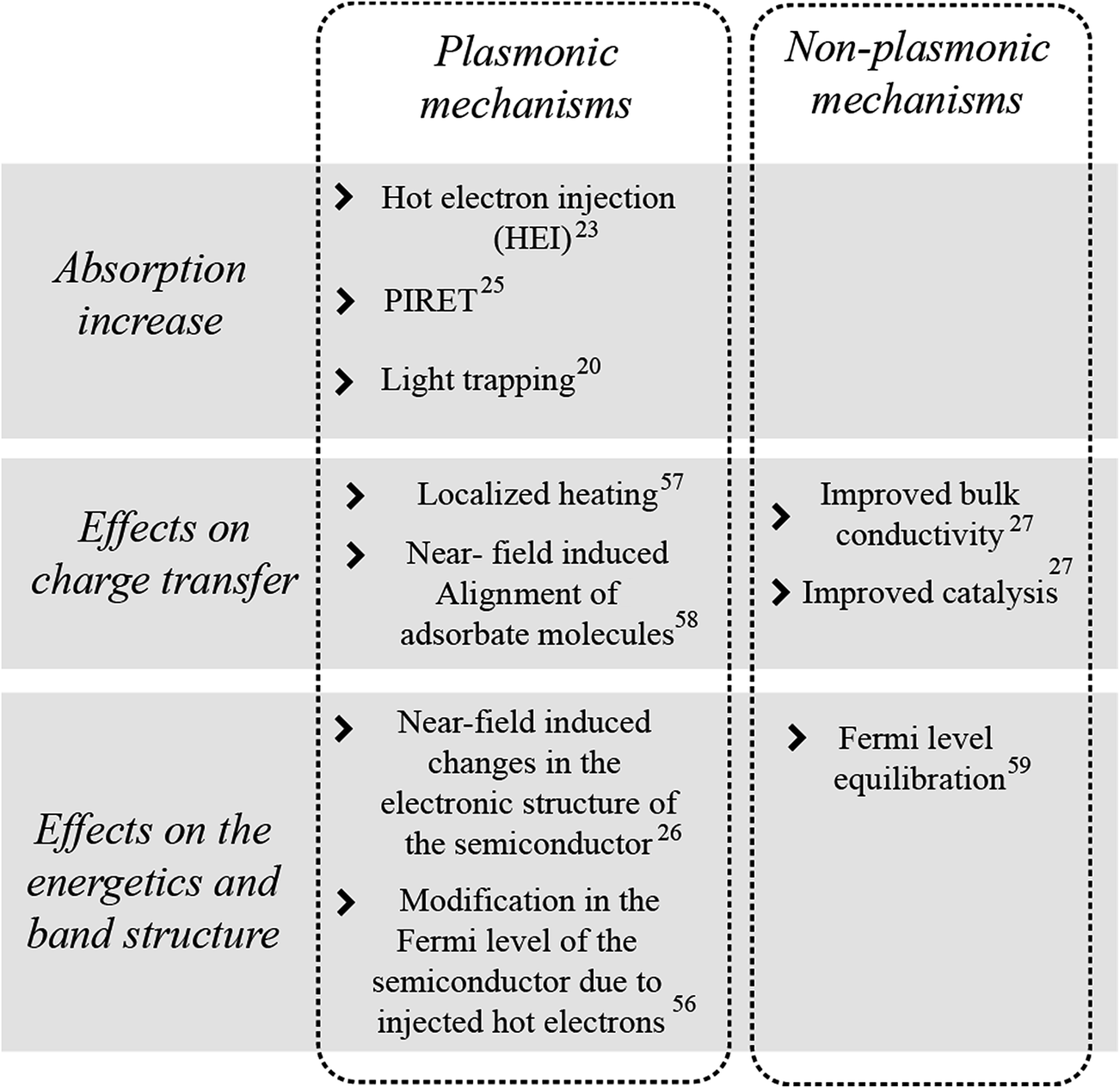 | ||
| Fig. 7 Summary of proposed effects of metal NPs on semiconductors for photoelectrochemical water splitting.20,23,25–27,56–59 | ||
4. Plasmonic energy transfer mechanisms
4.1. Hot electron injection (HEI)
Hot electrons are generated through non-radiative damping and hot electron injection (HEI) is therefore best exploited by light absorbing NPs. Fig. 8 shows a more detailed illustration of this mechanism. When the surface plasmons decay through intraband excitations within the conduction band, the excited electrons (hot electrons) obtain energies higher than the metal Fermi energy (EF; cf.Fig. 8).60,61 For plasmonic NPs smaller than 20 nm the hot electron exhibit energies (EH) within the range EF < EH < EF + ħω, while larger particles exhibit much smaller hot electron energies close to EF.62 If the energy of the hot electrons are larger than the interface Schottky energy barrier, the hot electrons can be transferred to the conduction band of the semiconductor.23,51,61,63–67 Charge neutrality in the metal NP is restored by removing the “hot hole” with an oxygen evolution catalyst (OEC) or an electron-donor solution (in the case of an n-type semiconductor). Excited electrons with energies lower than the Schottky barrier relax through, for instance, electron–electron and electron-phonon collisions (releasing heat).68 Therefore, the efficiency of the HEI mechanism is expected to decrease with increasing Schottky barrier energies, which depend on the energetics of the selected metal/semiconductor system. However, having energies larger than the Schottky barrier is by no means the only requirement for a hot electron to be injected to the conduction band of the semiconductor. The hot electron also needs to reach the surface of the NP, before undergoing another relaxation process.24 Further limitations come from the non-ideal electron-acceptor ability of the semiconductor (i.e., limited density of states in the conduction band) and the non-ideal electron-donor ability of the OEC/electrolyte that replaces the injected hot electrons.24,69–71 The above limitations significantly affect the efficiency of HEI and it is of great importance to theoretically and experimentally study each limitation individually. One of the main challenges to experimentally study the HEI efficiency comes from the fact that the measured hydrogen/oxygen evolution in a plasmonic NP/semiconductor photoelectrode not only come from the HEI process (due to the NP light absorption) but also from light absorption of the semiconductor itself. Therefore, strategies must be developed to accurately decouple these two contributions before attempting the optimization of HEI. Two recent publications made key contributions to tackle this issue using two different approaches. Mubeen et al.,23 fabricated a Au nanorod/TiO2 composite system, where the TiO2 layer was so thin that its only role was to remove the hot electrons from the nanorod (electron filter) and did not contribute to the measured photocurrent. Chen et al.26 used a different strategy based on a Au NP/ZnO composite and tested its photoelectrochemical ability to split water by illuminating it only with visible light that has lower energies than the ZnO band gap. That ensured that only photocurrent related to the HEI mechanism was measured. We start by reviewing the work by Mubeen et al. in detail in order to gain further insights to the HEI mechanism. | ||
| Fig. 8 (A) Plasmonic energy conversion: electrons from occupied energy levels are excited above the Fermi energy. (B) Hot electrons can be injected into a semiconductor by forming a Schottky barrier with the plasmonic nanostructure. Hot electrons with energies high enough to overcome the Schottky barrier φSB = φM − χS are injected into the conduction band EC of the neighbouring semiconductor, where φM is the work function of the metal and χS is the electron affinity of the semiconductor. Reprinted in part with permission from ref. 24. Copyright 2014 Macmillan publishers limited. | ||
Mubeen et al. fabricated an autonomous plasmonic solar water splitting device where the oxygen and hydrogen evolution reaction take place on the NP-semiconductor composite without the use of external wires and without applying a bias voltage. This device consists of an array of vertically aligned gold nanorods in an aluminium oxide template. Fig. 9A and B, show an illustration and a transmission electron microscope (TEM) image of one of the nanorods, respectively. The plasmonic rod is capped with a thin layer of crystalline TiO2, which in turn is decorated with a hydrogen evolution catalyst (Pt NPs). On the side of the nanorod a cobalt-based oxygen evolution catalyst is deposited. In this device, all the charge carriers are derived from surface plasmons (through HEI) and the semiconductor works only as a hot electron filter as depicted in Fig. 9C. Using this approach, once the hot electrons and holes are separated, they migrate to the corresponding catalysts to carry out the water splitting half reactions. The autonomous device was operated with a 1 M potassium borate electrolyte (pH 9.6) under visible light illumination (λ > 410 nm), exhibiting an external quantum efficiency (EQE) of ∼0.1% (averaged over the visible portion of the solar spectrum). Several strategies were taken in this work to confirm that all the charges indeed came from the HEI mechanism and not from conventional TiO2 light absorption. One of them is shown in Fig. 10, where the hydrogen production of the device was measured under illumination with light of different spectral ranges. Under UV-dominated illumination (310 nm < λ < 520 nm), the hydrogen production rate is much lower than when the device is illuminated with visible light (λ > 410 nm or λ > 600 nm). The low performance under UV illumination confirms that conventional electron–hole excitation due to light absorption in the TiO2 does not contribute to the hydrogen generation under AM 1.5 irradiation, since TiO2 only absorbs light up to ∼380 nm. Therefore, this device is ideal to independently study the different processes that limit the HEI efficiency (e.g., electron-donor ability of the hydrogen evolution catalyst). Finally, this work reports no decrease in activity over 66 hours of solar irradiation. This excellent stability represents a great advantage for plasmon driven water splitting devices when compared with conventional short bandgap metal oxide semiconductors that decrease their performance over time due to corrosion.72,73
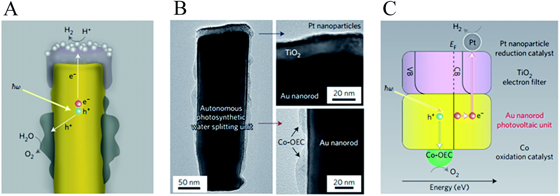 | ||
| Fig. 9 Structure and mechanism of operation of the autonomous plasmonic solar water splitter. (A) Schematic of the cross-section of an individual photosynthetic unit showing the inner gold nanorod, the TiO2 cap decorated with platinum nanoparticles, which functions as the hydrogen evolution catalyst, and the Co-OEC material deposited on the lower portion of the gold nanorod. (B) Corresponding transmission electron micrograph (left) and magnified views of the platinum/TiO2 cap (top right) and the Co-OEC (bottom right). (C) Energy level diagram superimposed on a schematic of an individual unit of the plasmonic solar water splitter, showing the proposed processes occurring in its various parts and in energy space. CB, conduction band; VB, valence band; EF, Fermi energy. Reprinted with permission from ref. 23. Copyright 2013 Macmillan publishers limited. | ||
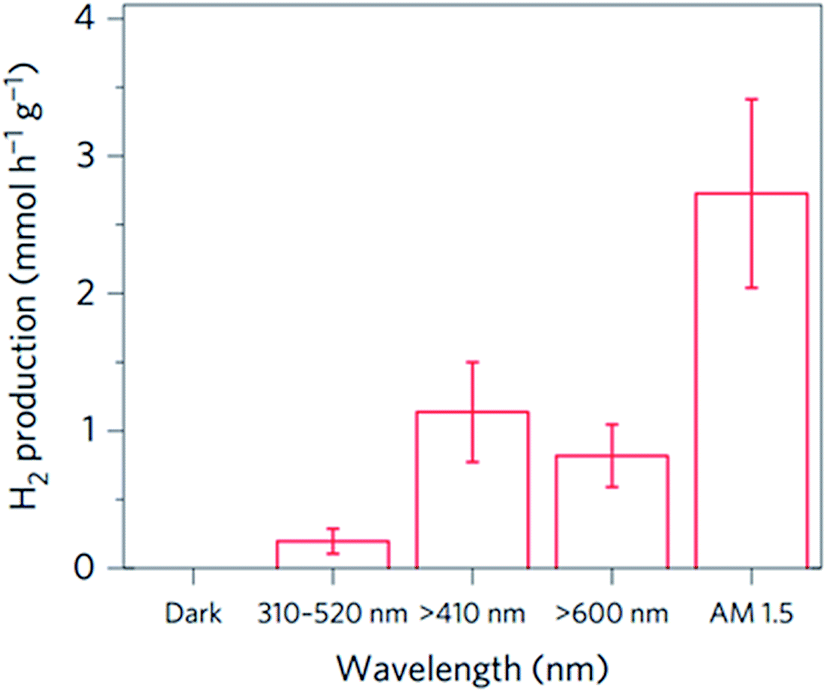 | ||
| Fig. 10 Hydrogen produced per hour with various illumination wavelengths, each determined from an experiment in which the device was continuously illuminated for 9 h. Reprinted with permission from ref. 23. Copyright 2013 Macmillan publishers limited. | ||
More recently, the same authors reported74 photo-production of hydrogen with a similar system for gold nanorods with different aspect ratios, exhibiting longitudinal absorption modes nearly throughout the solar spectrum (λ ∼ 400–1000 nm). In this work, instead of an electron donor oxygen evolution catalyst, methanol was added to the electrolyte as a sacrificial reactant. The authors show that by using nanorods with different aspect ratios the hydrogen production can be doubled compared with a device that uses nanorods of the same dimensions. The device presented a EQE of ∼0.1% (averaged over the entire solar spectrum) and showed good stability for over 200 hours of continuous operation.
Unlike in the previously described works, Chen et al.26 synthesized a NP/semiconductor composite where the semiconductor absorption contributes significantly to the composite's hydrogen generation. The NP/semiconductor composites used in this work consist of arrays of ZnO nanorods decorated with spherical gold NPs with an average size of less than 5 nm. These composites were used as the working electrode in a three electrode-based photoelectrochemical system, and cyclic voltammetry measurements under AM 1.5 solar simulation irradiation are shown in Fig. 11A. It is clear that the performance of the composite device increases with an increase in the plasmonic NP concentration, until an optimum NP loading of 9.8%. Fig. 11B, shows a similar type of experiment, but this time the sample was irradiated only with visible light (>420 nm). This visible light has lower energies than the semiconductor band gap and, as expected, no photocurrent was obtained in the cyclic voltammetry of the bare ZnO sample (cf.Fig. 11B). After NP deposition the photocurrent increased up to ∼0.3 μA cm−2 at 1 V vs. Ag/AgCl, which the authors attribute to the HEI mechanism. In order to further elucidate the HEI effect, wavelength dependent photocurrent measurements were performed and compared with the NP absorption spectra. Fig. 12 shows that the measured photocurrent presents a peak around 2.4 eV, which corresponds well to the NP plasmon absorption mode. This correlation between the photocurrent and the absorption spectra gives further evidence that the obtained photocurrent is due to a plasmonic effect. This type of comparison is now commonly used to prove plasmonic effects and has become an important tool in the plasmon driven water splitting field. However, it should be pointed out that hot electrons with sufficient energy to overcome the Schottky barrier may be excited also without plasmonic effects, via the photoelectric effect. Chen et al. also compared the measured photocurrent with the number of photoelectrons that derive from direct light excitation (photoelectric effect) and have sufficient energy to overcome the Schottky energy barrier. These photoelectrons (Fowler hot electrons) are calculated according to Fowler theory:
 | (5) |
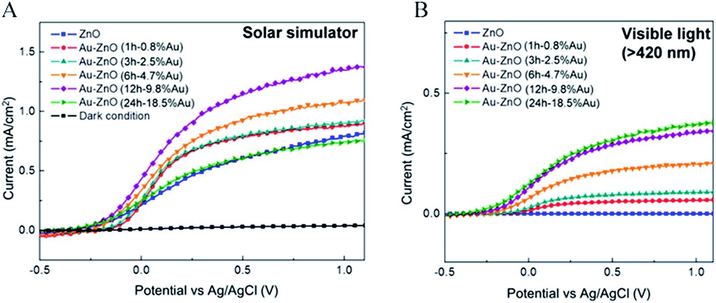 | ||
| Fig. 11 (A) Linear-sweep voltammograms of Au–ZnO photoelectrodes with nanoparticles deposited for various periods, and a dark scan, performed in a 0.5 M aqueous Na2SO4 with a pH of 6.8 under an AM 1.5 solar simulator. (B) Linear-sweep voltammograms of Au ZnO photoelectrodes with nanoparticles deposited for various periods, obtained under illumination by visible light (>420 nm). Reprinted with permission from ref. 26. Copyright 2012 ACS. | ||
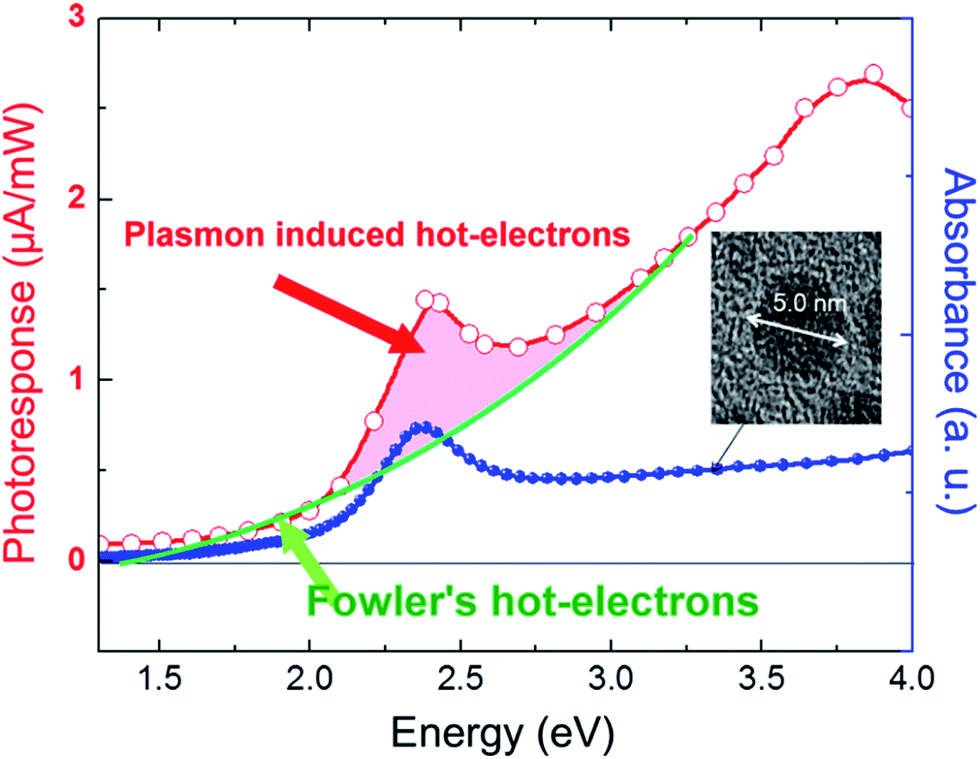 | ||
| Fig. 12 Absorption spectrum of Au nanospheres and plots of photocurrent versus wavelength, fitted to Fowler's law, indicating that photocurrent comprises mainly hot electron flow, with additional contribution from hot electrons that are injected from Au under plasmonic-induced irradiation that is amplified by localized surface plasmon resonance. Reprinted with permission from ref. 26. Copyright 2012 ACS. | ||
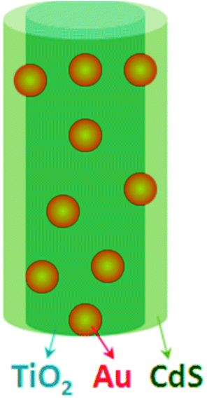 | ||
| Fig. 13 Illustration of the sandwich CdS–Au–TiO2 composite. Reprinted with permission from ref. 18. Copyright 2014 ACS. | ||
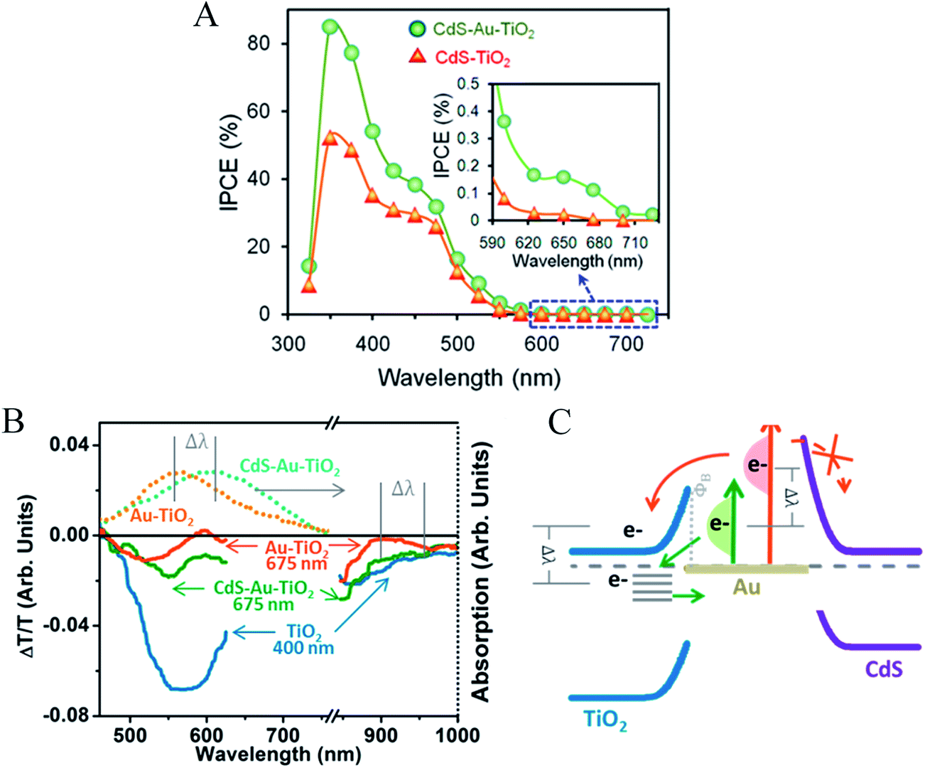 | ||
| Fig. 14 (A) IPCE. (B) NP absorption in Au–TiO2 and in CdS–Au–TiO2 (Top) and full-spectrum transient absorption signal at 20 ps after excitation (bottom). (C) The change in back-transfer dynamics and filling of the TiO2 electron-trap states without charge transfer into CdS is explained by the energy of the hot plasmonic electron distribution relative to the interfacial Schottky barrier. Reprinted with permission from ref. 18. Copyright 2014 ACS. | ||
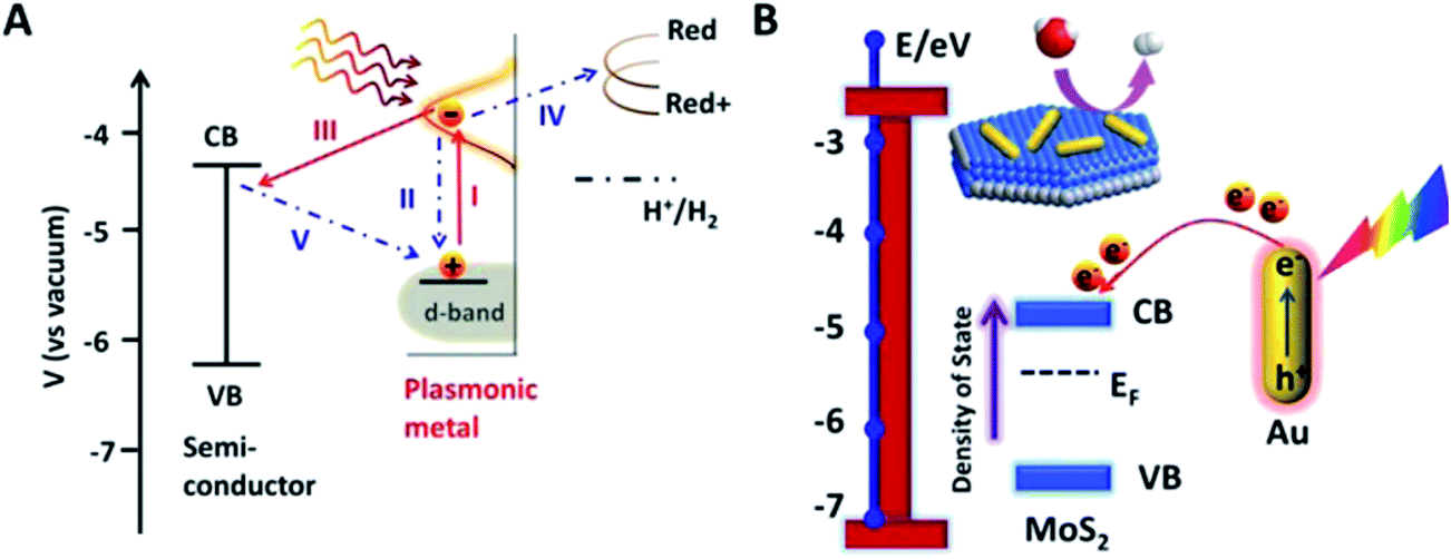
4.1.2.1. NP composition. As discussed above, the HEI efficiency highly depends on the hot electron energy. Hot electrons can be generated either by intraband or interband transitions. Recent theoretical studies78–81 have shown that interband transitions induced by visible light (from the d-band) result in high energy hot holes but low energy hot electrons (∼EF), due to the position of the d-band relative to the Fermi level in noble metals. By contrast, hot electrons generated by intraband transitions can have energies up to EF + ħω.62 Therefore, it is advantageous to use materials with a relatively large interband energy threshold to maximize the intraband excitation spectrum. Ag exhibits an interband energy of ∼3.7 eV and, therefore, only intraband transitions are expected when illuminated with visible light. Au on the other hand, has an interband energy of ∼2.3 eV and its HEI efficiencies may be limited by interband excitations when illuminated with violet, blue and green light.
The above reasoning holds for HEI over the Schottky energy barrier (as illustrated in Fig. 8), where the HEI efficiency depends on the hot electron energy. However, it has been recently proposed that low energy hot electrons (generated by interband transitions) can also be transferred to the semiconductor by tunnelling through the Schottky energy barrier.82 Further research must be undertaken to study the efficiency of this hot electron transfer process.
The material composition of the NP is of great importance in the design of HEI water splitting devices, because it affects three important HEI parameters: (i) LSPR frequency, (ii) Fermi level equilibration, and (iii) the energy of the resulting charge carriers. Even though materials other than Au and Ag have been used for HEI applications, including Pt83,84 and Al,30 we believe that alloy NPs are particularly promising for future HEI devices. The use of alloy NPs allows for fine-tuning of these three important parameters to fit the requirements of specific hot electron acceptor semiconductor for specific applications.
4.1.2.2. NP size. NPs of less than 20 nm are used as hot electron injectors, since their hot electrons exhibit high energies (up to EF + ħω),62 and can readily reach the NP surface where they are extracted. Since hot charge carriers created by intraband transitions have a mean free path of ∼10–40 nm,78 most of the generated hot carriers in these NPs (<20 nm) are expected to reach the surface before thermalization. In contrast, hot carriers created by interband excitations are expected to have much shorter mean free paths (∼1 nm)78 and, therefore, even smaller NPs (2–3 nm) are required for charge extraction. Particles smaller than 2 nm in size are called metal clusters, and exhibit a discrete molecule-like band structure. It has been reported that Au clusters with distinct highest occupied molecular orbital (HOMO)-lowest unoccupied molecular orbital (LUMO) gap can act like a semiconductor with short band gap.85 Even though this review focuses on plasmonic NPs, it is important to highlight that metal clusters can also be used as co-absorbers to enhance the absorption of metal oxides.86
4.1.2.3. NP shape. Varying particle shape enables tuning of the NP LSPR frequency, which makes possible to absorb and utilize light throughout the complete solar spectrum. In addition, it has been suggested that NP shape also affects the amount and location of generated hot carriers within the NP.87,88 Harutyunyan et al.87 studied the hot charge carrier dynamics with standard pump-probe measurements for different nanostructure geometries and reported ultrafast dynamics in nanostructures with “hot spots” (areas with greatly enhanced electromagnetic field). The authors ascribed this ultrafast response to an efficient generation of hot electrons from hot spots. In good agreement with this, Sousa-Castillo et al.88 showed that the photochemical response of TiO2 is enhanced to a larger extent when functionalized with nanostars than when functionalized with nanorods or spherical NPs. The high photocatalytic activity was ascribed to hot spots present around the spikes of the NP, which promotes the hot carrier generation near the NP-semiconductor interface and the subsequent HEI to the semiconductor.
As will be explained in the following section, the HEI mechanism is the only known plasmonic mechanism that can expand the absorption of a semiconductor water splitting device to longer wavelengths without depending on spectral overlap with the semiconductor. Therefore, if well-defined plasmonic NPs that absorb light beyond the semiconductor absorption edge are used, the HEI can be studied independently, as was done in the works discussed above. However, in most reports on plasmonic water splitting, an overlap between the semiconductor absorption and the NP absorption/scattering may give rise to many other plasmonic and non-plasmonic effects that simultaneously affect the semiconductor absorption and electrochemical properties.27,28,55,56,89–97 These ideas are discussed in the context of recent literature reviewed in the following two sections.
4.2. Light scattering, light concentration and PIRET
Unlike the HEI mechanism, the light scattering, light concentration and PIRET mechanisms do not transfer the plasmon energy by charge transfer, but radiatively or by a dipole–dipole interaction, inducing interband excitations in a neighbouring semiconductor. The benefits of these mechanisms in photoelectrochemical water splitting are illustrated in Fig. 15 for backside illumination (light reaching the semiconductor first). Most bare semiconductor films exhibit incomplete absorption and the transmitted light is unexploited (Fig. 15A). When the semiconductor is decorated with light scattering NPs (cf.Fig. 15B), the transmitted light interacts with the metal NPs, inducing surface plasmons that subsequently decay by scattering the photons back into the semiconductor. As a result, the optical path length through the semiconductor is increased, which increases its absorption and water splitting performance.22Fig. 15C illustrates a similar principle, where the transmitted light induces LSPR in the metal NP, which generates a highly localized electric field in the vicinity of the NP. This NP near-field can locally excite additional electrons from the valence band of the semiconductor to the conduction band (i.e., through the light concentration and PIRET mechanisms), again, improving the device performance.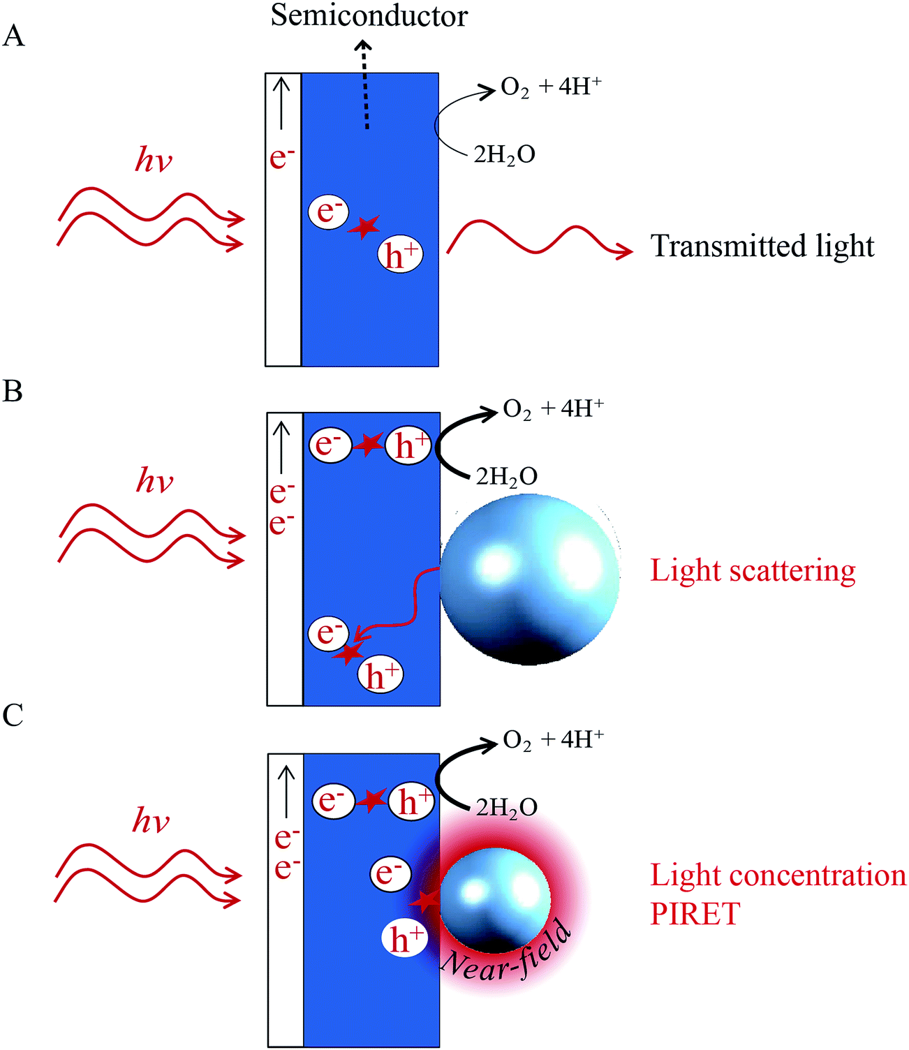 | ||
| Fig. 15 Illustration of absorption enhancement in a water splitting photoanode due to light scattering, light concentration and PIRET. | ||
Essentially, light concentration and light scattering only increase the interaction of light with the semiconductor by concentrating it and by increasing its path through the semiconductor. Therefore, these mechanisms are called light trapping or photonic enhancement mechanisms. They can increase the absorption of the semiconductor for plasmonic NP systems with resonances with energies above the optical band gap edge (OBGE) of the semiconductor.46,51 PIRET, as with light concentration and light scattering, also occur at wavelengths that overlap with the semiconductor's absorption spectra. However, PIRET has also been demonstrated to generate electron–hole pairs below the semiconductor OBGE, suggesting strong dipole–dipole coupling with band edge states that are optically inaccessible (see Section 4.2.2).25,74
 | ||
| Fig. 16 (A) Back illumination absorption increase in the BiVO4 spectra upon deposition of 65 nm Ag NPs. (B) Back illumination Incident photon to current conversion efficiency (IPCE) measurements before and after 65 nm Ag NP functionalization. Reprinted with permission from ref. 22. Copyright 2016 Wiley-VCH. | ||
Cushing et al.25 discovered that, unlike direct light excitation, the plasmon's strong dipole moment can also locally induce excitations below the OBGE, extending the light utilization of the semiconductor to longer wavelengths. In this near-field mechanism, called PIRET, the surface plasmon decays through a non-radiative dipole–dipole energy transfer to the semiconductor, resulting in electron–hole excitations in the semiconductor. This mechanism was studied in an Au–SiO2–Cu2O sandwich NP (Fig. 17A) by transient absorption spectroscopy (TAS) and wavelength dependent photocatalysis. In this study the insulating SiO2 layer prevent HEI from the metal to the semiconductor outer layer (i.e., Cu2O), while the near-field can still penetrate the SiO2 layer and interact with the semiconductor. Wavelength dependent photocatalytic measurements showed a clear enhancement in the conversion efficiency at energies both above and below the semiconductor OBGE (Fig. 17B) when compared with the efficiency of the bare semiconductor (Fig. 17C). These results, accompanied by transient analysis and theoretical calculations, lead the authors to identify the PIRET mechanism as being responsible for the observed enhancement. Two important advantageous characteristics of PIRET are that (i) unlike light trapping mechanisms, it allows for absorption enhancement of the semiconductor at energies below its OBGE due to dipole–dipole coupling to weak band edge states (yet still requiring a spectral overlap with the semiconductor absorption) and (ii) unlike HEI, it does not require specific band energy alignment of the semiconductor with respect to the Fermi level of the plasmonic NP. The discovery of PIRET modifies the previous understanding of the light concentration mechanism since the localization of the incident electromagnetic field in the vicinity of the NP (NP near-field) cannot only induce electron hole-pairs radiatively (proportionally to the square of the electric field) but can also non-radiatively induce electron–hole pairs below the OBGE in the near-field through a dipole–dipole interaction (PIRET). Since PIRET is a relatively new discovery, most water splitting publications that use small light absorbing NPs to locally increase the semiconductor absorption discuss their results solely under the context of the light concentration mechanism, and should be revisited including PIRET in the interpretation.
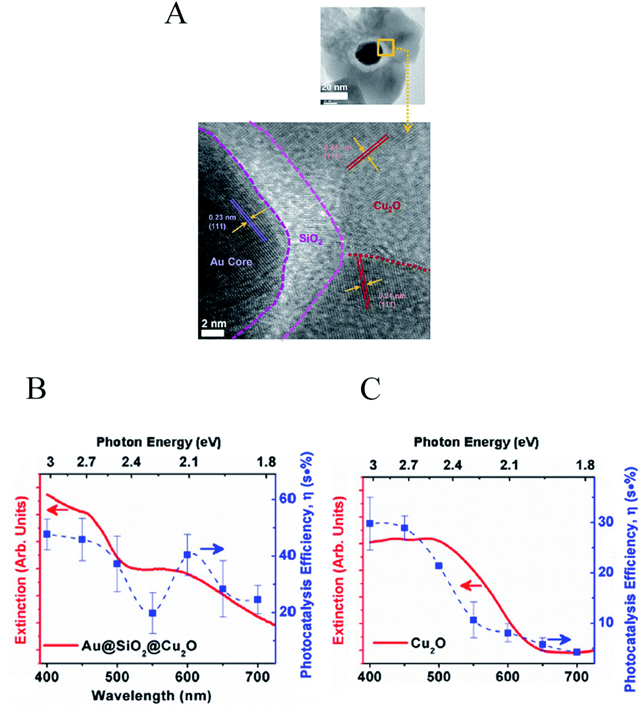 | ||
| Fig. 17 (A) Au@SiO2@Cu2O sandwich structure (top) and an enlargement of the micrograph for the interface regions of the sandwich structure shows the various crystal orientations (bottom). Ultraviolet-visible spectra and photocatalytic action spectra for (B) Au@SiO2@Cu2O and (C) Cu2O. Reprinted with permission from ref. 25. Copyright 2012 ACS. | ||
For small light absorbing NPs, it is still not clear what percentage of the surface plasmons energy is transferred to the semiconductor through near-field mediated energy transfer (e.g., PIRET) and what percentage is through HEI. However, recently, Cushing et al.54 shed light on this issue by studying the charge carrier dynamics in TiO2 coated silver NPs with transient absorption spectroscopy (TAS). The authors report that in these coated NPs, HEI and PIRET take place simultaneously, with PIRET being the more prominent mechanism. This points out the fact that the HEI is generally more limited than PIRET, due to its strict dependence on several operating parameters (cf. Section 4.1., e.g., Schottky energy barrier). In the same work, Cushing et al., also studied other coated NP architectures with transient absorption analysis, finding the conditions needed for HEI and PIRET to occur in a plasmonic NP/semiconductor composite as summarized in Fig. 18. Their findings confirm that (i) unlike HEI, PIRET only takes place at the region of the spectrum where there is spectral overlap between the semiconductor and the NP and (ii) unlike HEI, PIRET can occur even when there is not direct contact between the NP and the semiconductor, since the NP near-field can penetrate through a thin insulating layer. Due to the latter, plasmonic NPs with an insulating coating block the HEI mechanism and, therefore, facilitates the study of PIRET and the light concentration mechanisms. Combined with additional reasons described below, this has led to a significant number of publications that use plasmonic NPs coated with an insulating layer in NP/semiconductor composite water splitting devices.55,89,104
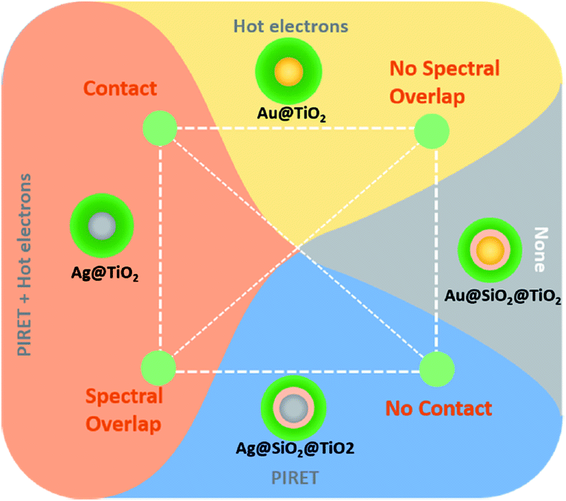 | ||
| Fig. 18 Variables that control the possible plasmonic enhancement near-field mechanisms for extending photoconversion. Connecting the line between the properties of the given core@shell nanoparticle gives the corresponding enhancement mechanisms present. Reprinted with permission from ref. 54. Copyright 2015 ACS. | ||
Thomann et al.,104 functionalized Fe2O3 films with 50 nm gold NPs coated with a 10 nm shell of SiO2 in two configurations that have the (i) NPs embedded in the film and (ii) the NPs at the semiconductor–electrolyte interface. Both configurations showed a clear enhancement in the wavelength dependent photocurrent compared with the bare semiconductor sample. The spectra of this photocurrent enhancement closely followed the simulated absorption increase due to the plasmonic NPs, which evidenced a plasmonic effect for both configurations. This photocurrent enhancement was assigned, with the help of full-field electromagnetic simulations, to the semiconductor absorption increase in the vicinity of the plasmonic NPs. However, for configuration (ii) (NPs at the semiconductor surface) a background wavelength independent enhancement was seen, which could not be explained by plasmonic mechanisms such as PIRET or light trapping. The authors speculate that such wavelength independent enhancement arise from surface effects such as catalytic effects on water oxidation by the NPs.
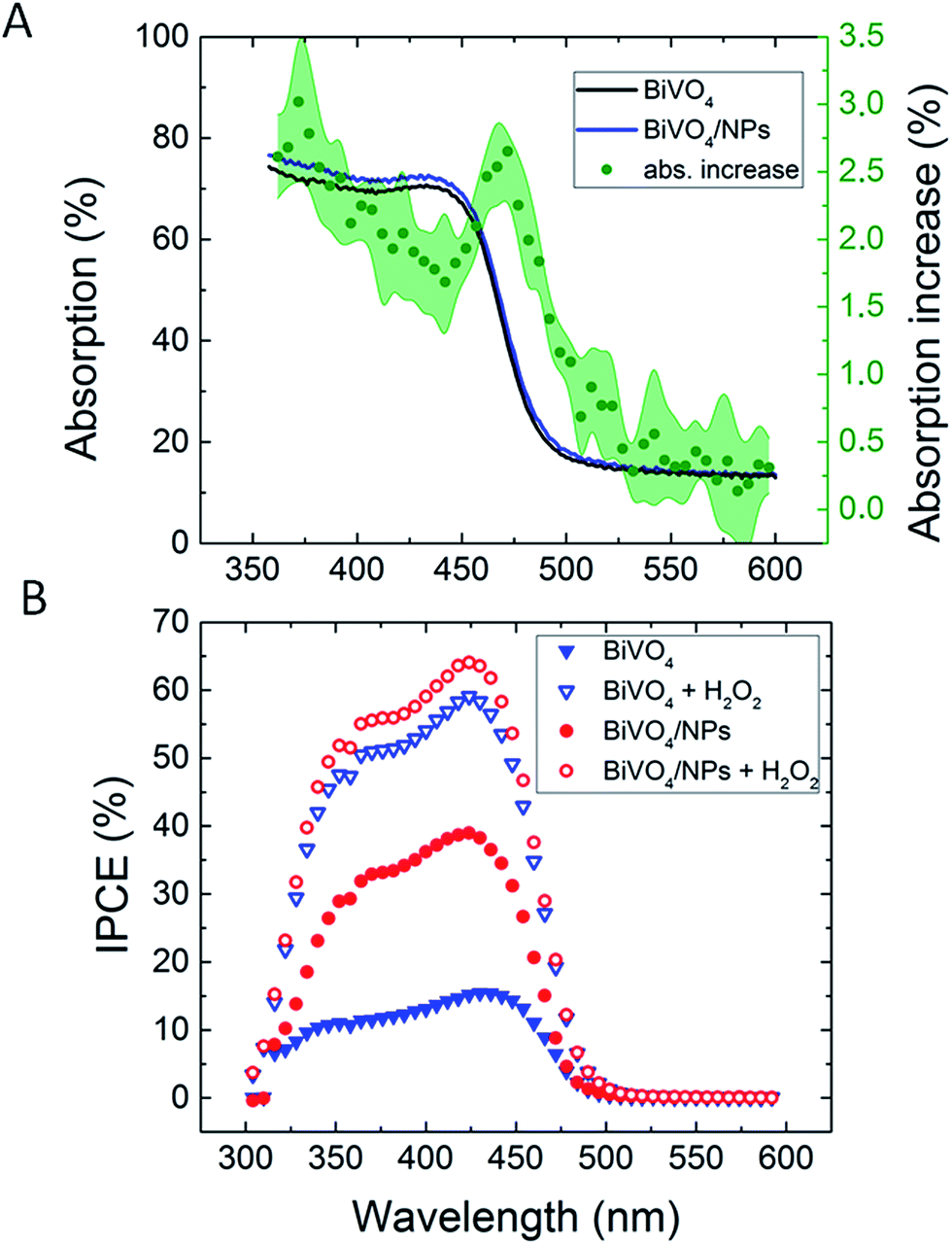
Abdi et al.,55 decorated the surface of BiVO4 photoanode films with 50 nm SiO2 coated Ag NPs and found a 2.5-fold photocurrent enhancement under simulated sun illumination at 1.23 V vs. RHE. The authors ascribed this enhancement to both catalytic and optical effects due to the decorating plasmonic NPs. By adding a hole scavenger (H2O2) in the electrolyte, the authors were able to identify the absorption enhancement contribution to the total IPCE enhancement. An absorption enhancement of 33% was in good agreement with full-field electromagnetic simulations and was ascribed to far-field (light scattering) and, in a lesser extent, to near-field effects. As can be seen in Fig. 19, the IPCE increase reported in this work is larger than 15% IPCE at ∼425 nm. Such a large IPCE enhancement can be explained by the significant overlap between the semiconductor and the plasmonic NPs absorption spectra, which is a requirement for the light trapping mechanisms (concentration and scattering of light) and PIRET. In order to increase such spectral overlap, the NPs' geometry,89 composition89 and their spatial distribution (e.g., dimer formation22,30) can be modified. As example, Erwin et al.89 synthesized Au–Ag core–shell nanostructures to expand the absorption overlap of the NP with the semiconductor. When compared with the absorption of spherical NPs, the Au–Ag core–shell nanostructures (e.g., nanopyramids) exhibited a second absorption mode and broader absorption spectra. These particles were coated with a thin insulating layer of SiO2 and embedded in mesoporous TiO2 photoanodes. The absorption and IPCE of the bare TiO2, Au–Ag core–shell nanostructures/TiO2 composite and spherical Au NPs/TiO2 composite are shown in Fig. 20. The Au–Ag core–shell nanostructures clearly increased the absorption of the photoanode in a larger extent than the spherical Au NPs, throughout the measured range. Accordingly, the IPCE enhancement was also increased in a larger extent for the Au–Ag core–shell nanostructures/TiO2 composite. This shows that broadening the absorption overlap between the NP and the semiconductor by modifying the NP geometry and composition can efficiently extend the action of light trapping and PIRET. However, the obtained IPCE increase was low (∼0.01%, Fig. 20B) due to the poor visible light absorption of TiO2 (Fig. 20A). In the same work, the authors also characterized their samples by measuring the photocurrent under solar simulated light, modulated at different light intensities (i.e., from 50 mW cm−2 to 300 mW cm−2). While the bare photocurrent of the semiconductor showed a half order dependency to the light intensity, the photocurrent of the functionalized composites showed a first order dependency. This phenomenon was previously reported46 for TiO2 samples functionalized with Ag NPs, and can be explained by the near-field mechanisms.20 These mechanisms concentrate the light at the semiconductor/electrolyte interface, increasing the generation of charges near the semiconductor surface where the space charge region is located. Therefore, all the near-field induced charges are efficiently separated due to the built-in electric field in the space charge layer. Consequently, in composites where the near-field induced charges are prominent contributors to the total photocurrent, the bulk charge separation is not a limiting step and the photocurrent shows a first order dependence on light intensity. This important feature of promoting the generation of charges at the space charge region was also studied by Valenti et al.,28 by comparing the light absorption increase of CuWO4 films when plasmonic NPs were deposited either (i) at the back contact/semiconductor interface or (ii) at the semiconductor/electrolyte interface. It was found that the increase in absorption was more effectively extracted as photocurrent when the NPs were placed at the surface of the semiconductor (ii). This result can again be explained by the efficient separation of the near-field induced charges at the space charge region. Naldoni et al.105 also studied the effect of plasmonic NPs at the semiconductor–electrolyte interface and their findings suggest that both decreasing the interparticle distance and partially embedding the NPs in the semiconductor can enhance the light concentration in the semiconductor and its photocatalytic activity.
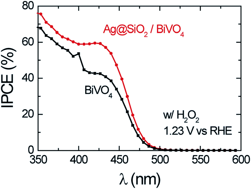 | ||
| Fig. 19 IPCE of bare BiVO4 and Ag@SiO2/BiVO4 at 1.23 V vs. RHE in the presence of 0.5 M H2O2 in the electrolyte. Reprinted with permission from ref. 55. Copyright 2014 RSC. | ||
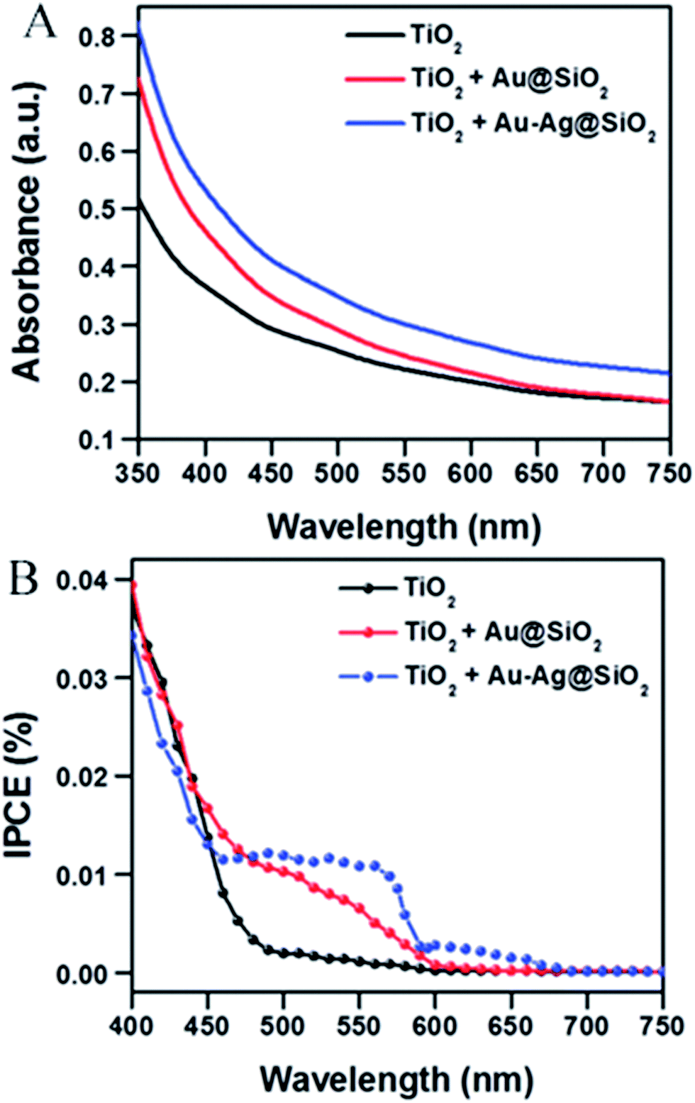 | ||
| Fig. 20 (A) Absorption spectra showing enhancement in light absorption with Au–Ag@SiO2 nanostructures (blue) and Au@SiO2 nanoparticles (red) embedded within the mesoporous TiO2 photoanodes relative to TiO2 only anodes (control, black). (B) IPCE curves of nonenhanced (TiO2 only) and plasmon enhanced photoanodes. The plasmon enhanced photoanodes are at the optimized concentration. Reprinted with permission from ref. 89. Copyright 2014 RSC. | ||
It is important to highlight that the near-field induced charge carriers are not only well separated (due to the electric field of the space charge region) but also the hole (in the case of n-type semiconductors) can readily reach the semiconductor/electrolyte interface in the vicinity of the NP, where other plasmonic or non-plasmonic effects can enhance its injection efficiency to the electrolyte (cf. Section 5.1). Therefore, the light concentration and PIRET effects are promising tools that could effectively enhance the absorption, bulk separation and injection efficiency to the electrolyte.
In addition to discrete NPs, nanotextured and flat metallic films have also been used to increase the semiconductor light absorption at specific regions of a neighbouring semiconductor.90,106,107 The increase in absorption for such systems is (i) related to the evanescent fields of the surface plasmon polaritrons (SPPs) of nanotextured films,90,108 or (ii) due to the ability of metal films to reflect light and generate resonant cavity modes.107 In both cases, the films can also be used as back contact current collector in the water splitting device.90,107 A synergetic approach combines the LSPR effects provided by plasmonic NPs at the electrolyte–semiconductor interface with additional enhancement mechanisms provided by a metallic film used as back contact. Fang et al.106 showed that this configuration enables light to be efficiently trapped by scattering-reflecting back and forth through the semiconductor between Au nanodisk and a Au mirror film.
Table 1 summarizes the most important physical, optical and electronic characteristics of the above described LSPR mechanisms (i.e., light scattering, light concentration, HEI and PIRET) that can increase the overall absorption of a semiconductor photoelectrode. This table can be used in the design of a plasmonic NP/semiconductor composite photoelectrode to optimize the performance of the semiconductor or to further elucidate the nature of these plasmonic mechanisms.
| Light scattering | Light concentration | PIRET | HEI | |
|---|---|---|---|---|
| Origin of enhancement | Photonic enhancement | Dipole–dipole energy transfer | Charge transfer | |
| NP-semiconductor spectral overlap | Required | Required | Not required | |
| Enhancement above optical bandgap edge | ✓ | ✓ | ✓ | |
| Enhancement below optical bandgap edge | ✗ | ✓ | ✓ | |
| NP-semiconductor contact | Not required | Not required | Required | |
| Alignment of band energies | Not required | Not required | Required | |
5. Electrochemical effects
Besides light absorption, plasmonic NP can also induce effects in the semiconductor's charge transfer properties (cf. Subsection 5.1.), energetics (cf. Subsection 5.2.), and band structure (cf. Subsection 5.3.). In this section we discuss these plasmon-induced and non-plasmon-induced NP effects that do not increase light absorption, but instead facilitate the electrochemical processes in a semiconductor-based water splitting device.5.1. Effects on charge transfer
Depending on where the plasmonic NPs are placed in the semiconductor device (embedded or on the surface), the NPs can affect the bulk and/or surface charge transfer processes that the photogenerated charge carriers undergo in the semiconductor to carry out the water splitting half reactions.27,28 In the case of n-type semiconductor photoanodes, the photogenerated holes first move through the semiconductor towards the semiconductor surface (bulk charge transport). Subsequently, the hole needs to be transferred from the valence band to the semiconductor surface, where the hole is injected to the electrolyte to evolve oxygen. In particular this last step (charge injection from the semiconductor surface to the electrolyte) has often been ascribed as main responsible for photocurrent increase upon plasmonic NP functionalization.22,27–29,109–113 Haro et al.,27 obtained a significant increase in the catalysis and, in a lesser extent, an increase in the bulk conductivity after embedding gold NPs in a mesoporous TiO2 photoanode. After discarding HEI and light trapping mechanisms (based on PEC characterization), the authors studied the influence of the NPs on the bulk conductivity, chemical capacitance and surface charge transfer resistance of the TiO2 with electrochemical impedance spectroscopy (EIS) analysis. In this technique, the impedance (complex voltage to current ratio) spectrum of the system is obtained by applying a bias AC voltage to the PEC cell at different frequencies and recording the current response. Subsequently, the impedance spectrum is modelled with an equivalent circuit (EC), consisting of capacitors and resistors, that represents the limiting transport processes in a well-known PEC system. Haro et al.,27 used a well-established transmission line model as EC to fit the impedance spectra at different applied potentials. The parameters for the surface charge transfer, chemical capacitance and bulk conductivity were extracted from the fittings, as shown in Fig. 21. It can be clearly seen that the charge transfer resistance at the surface progressively decreased with the NP load in the photoanode. The chemical capacitance also increased upon NP functionalization, which is explained in this work by the increase of the density of states due to the gold NPs. Finally, Fig. 21C shows that the bulk conductivity slightly increased with the NP load.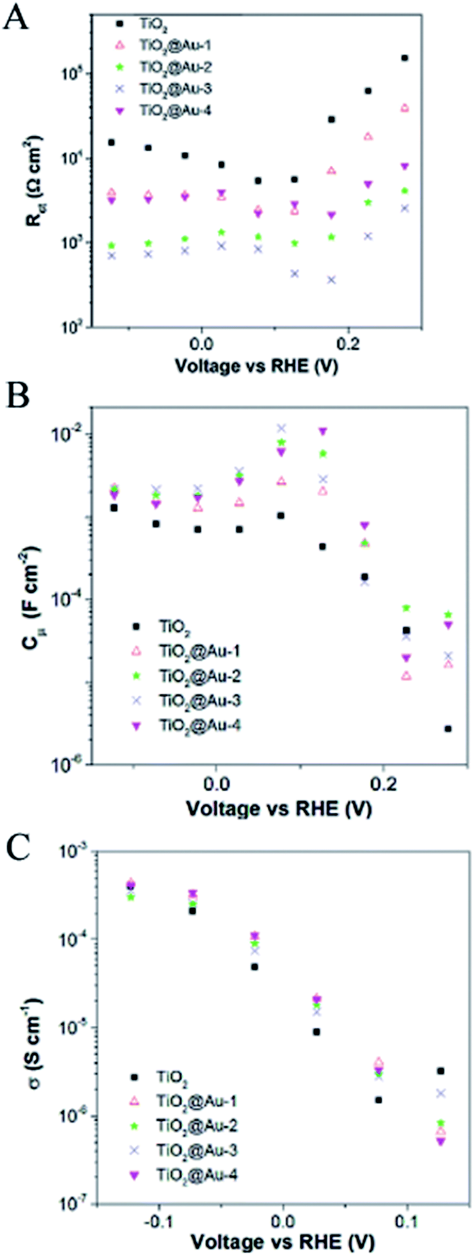 | ||
| Fig. 21 (A) Charge transfer resistance, (B) chemical capacitance, and (C) conductivity of mesoporous TiO2 films without and with different loading of Au NPs under illumination at 100 mW cm−2. The conductivity has been only calculated in the potential range where the transmission line is observed. Reprinted with permission from ref. 27. Copyright 2014 Elsevier Ltd. | ||
The increase in the charge carrier injection to the electrolyte could be due to the inherent catalytic properties of the metal, Fermi level equilibration59 (cf. Section 5.2.1.) or due to plasmonic effects, such as plasmonic heating,57 improved adsorption of polar molecules that align in the direction of the NP near-field58 and hot electron induced activation of co-catalysts.114 While EIS is a powerful tool that allows the ability to quantify the resistance of the charge injection to the electrolyte, other techniques must be developed in order to elucidate and distinctly recognize the different plasmonic and non-plasmonic effects that facilitate the charge transport processes. These charge transfer effects are of extreme importance when they occur in combination with plasmonic mechanisms that increase the absorption of the semiconductor, since for this case the NP plays the dual role of (i) light absorber and (ii) co-catalyst. This dual effect has already been demonstrated in different NP/semiconductor systems where the NP facilitate the charge carrier transport and also enhance the absorption through HEI18 or light trapping.22,40 In particular for near-field effects (light concentration and PIRET) occurring near the semiconductor surface, the additional plasmonic induced charge carriers (i) are well separated due to the space charge region, (ii) more readily reach the semiconductor surface, and (iii) exhibit enhanced charge injection to the electrolyte due to the enhanced catalysis near the NP. In this way, near-field induced charge carriers are expected to efficiently contribute to the overall photocurrent.
5.2. Effects on energetics
 | ||
| Fig. 22 Fermi level equilibration in a semiconductor–metal nanocomposite system. Reprinted with permission from ref. 59. Copyright 2004 ACS. | ||
A clear correlation between the extent of the negative induced Fermi level shift and the increased catalytic activity was shown by Subramanian et al.59 The authors decorated TiO2 NPs with Au NPs of different diameters (i.e., 3-, 5- and 8 nm) and found that decreasing NP size consistently increased the Fermi level negative shift and the photocatalytic activity of the composite. The increase of the Fermi level shift with decreasing NP size could be explained by the discrete nature of the energy levels in Au NPs, which results in a larger shift in energy level per stored electron for the smaller NPs.59
This subsection shows that metallic plasmonic NPs can not only increase the absorption of the semiconductor and improve its charge transfer properties, but they can also alter its electronic band energetics. Since properties like the plasmonic NP size determine the efficiency of both (i) plasmonic mechanisms that increase the semiconductor absorption, and (ii) non-plasmonic mechanisms that improve the energetics, a trade-off typically needs to be made according to the specific semiconductor limitations.
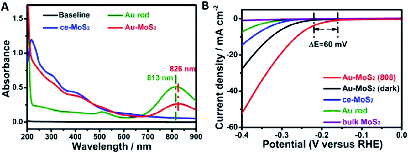 | ||
| Fig. 23 (A) UV-vis spectra of MoS2 (ce-MoS2) nanosheet, gold nanorod and Au–MoS2. (B) Hydrogen evolution reaction polarization curves obtained on several catalysts as indicated. Reprinted with permission from ref. 56. Copyright 2015 ACS. | ||
 | ||
| Fig. 24 (A) Different plausible hot electrons transfer pathways likely to occur during SPR. (B) Schematic Au–MoS2 and energy level diagram illuminating hot electrons injection and change of MoS2 Fermi level. Reprinted with permission from ref. 56. Copyright 2015 ACS. | ||
5.3. Effects on band structure
Finally, Chen et al.,26 studied the influence of gold NPs' near-field on the conduction/valence band of ZnO nanorods (same system discussed above in Section 4.1.) with X-ray absorption near edge structure (XANES). In this study, the gold NPs (with sizes of 4.7 nm ± 0.7 nm) were sitting uniformly on the surface of the ZnO nanorods. With XANES the authors observed a significant increase in the ZnO conduction band vacancies under plasmon-induced illumination, which can promote the separation of photogenerated electrons and holes. Such changes in the band structure near the NP/semiconductor interface were ascribed to the NP near-field. Therefore, the authors show that two advantageous plasmonic effects can occur in a plasmonic NP/semiconductor composite: (i) near-field induced generation of vacancies in the conduction band, and (ii) absorption increase through HEI (cf. Section 4.1.).6. Conclusions and outlook
Significant progress has been made in the last several years to elucidate the mechanisms (i.e., light scattering, light concentration, PIRET and HEI) by which plasmonic NPs can improve the solar light utilization of semiconductor photoelectrodes for efficient solar water splitting. Research on metal oxide water splitting photoelectrodes, which exhibit good catalytic activity and stability in aqueous media, benefits particularly from these new plasmonic mechanistic insights to circumvent the specific optical weaknesses of the different metal oxides. Table 1 summarizes some of the most important characteristics of each plasmonic mechanism that can enhance the light utilization in NP/semiconductor water splitting devices. As shown in this table, PIRET and HEI are mechanisms that can extend the light utilization of metal oxide photoelectrodes with large bandgap energies to the visible and near-infrared light. In particular, the HEI mechanism, whose efficiency is independent of the semiconductor absorption, allows for light harvesting of the entire solar irradiation spectrum by, for example, using rod NPs with different geometrical aspect ratios that collectively absorb light throughout the solar irradiation spectrum. However, the HEI mechanism suffers from many requirements, including the adequate alignment of the semiconductor band energies with respect to the Fermi level of the metal NP, which restricts its use to a limited number of material combinations. By contrast, photonic enhancements and PIRET do not require any band alignment, but their efficiency strongly depends on the NP-semiconductor spectral overlap. Therefore, following the great advances in the synthesis of well defined NPs and NPs systems (e.g., NP dimers, NP-metallic films systems, etc.) with predefined absorption spectra, more research needs to be directed towards ideal spectral overlap to achieve complete light absorption in promising new metal oxides with short band gaps by means of photonic enhancement and PIRET.While significant progress has been made in the understanding of the mechanisms to increase the light utilization of metal oxides, less attention has been paid to other roles that plasmonic NPs play when used in high performing metal oxide photoelectrodes (e.g., as a catalyst, co-catalyst, recombination centers, etc.). In particular, metal oxide photoelectrodes operating at low applied biases are often limited by poor bulk or interfacial charge transfer processes that are highly sensitive to the presence of metal NPs. In order to obtain a real optical contribution of plasmonic NP in efficient plasmonic NP/semiconductor water splitting devices, a better understanding of the NP charge transfer and energetics effects in the semiconductor must be further elucidated.
Acknowledgements
Financial support from the following institutions is gratefully acknowledged: NWO (VENI project granted to Dr Wilson A. Smith), the Wenner-Gren Foundations, the Swedish Research Council, the Swedish Foundation for Strategic Research, the Royal Swedish Academy of Sciences, the ÅForsk Foundation and the Swedish Government Strategic Research Area in Materials Science on Functional Materials at Linköping University (Faculty Grant SFO-Mat-LiU No 2009 00971).References
- A. Fujishima and K. Honda, Nature, 1972, 238, 37–38 CrossRef CAS PubMed.
- P. J. Boddy, J. Electrochem. Soc., 1968, 115, 199–203 CrossRef CAS.
- K. Sivula and R. van de Krol, Nature Reviews Materials, 2016, 1, 15010 CrossRef.
- K. Maeda and K. Domen, J. Phys. Chem. Lett., 2010, 1, 2655–2661 CrossRef CAS.
- M. A. Butler, R. D. Nasby and R. K. Quinn, Solid State Commun., 1976, 19, 1011–1014 CrossRef CAS.
- J. Su, L. Guo, N. Bao and C. A. Grimes, Nano Lett., 2011, 11, 1928–1933 CrossRef CAS PubMed.
- R. K. Quinn, R. D. Nasby and R. J. Baughman, Mater. Res. Bull., 1976, 11, 1011–1017 CrossRef CAS.
- A. Kay, I. Cesar and M. Grätzel, J. Am. Chem. Soc., 2006, 128, 15714–15721 CrossRef CAS PubMed.
- J. Y. Kim, G. Magesh, D. H. Youn, J.-W. Jang, J. Kubota, K. Domen and J. S. Lee, Sci. Rep., 2013, 3, 2681 Search PubMed.
- J.-N. Nian, C.-C. Hu and H. Teng, Int. J. Hydrogen Energy, 2008, 33, 2897–2903 CrossRef CAS.
- A. Paracchino, V. Laporte, K. Sivula, M. Grätzel and E. Thimsen, Nat. Mater., 2011, 10, 456–461 CrossRef CAS PubMed.
- F. F. Abdi, L. Han, A. H. M. Smets, M. Zeman, B. Dam and R. van de Krol, Nat. Commun., 2013, 4, 2195 Search PubMed.
- T. W. Kim and K.-S. Choi, Science, 2014, 343, 990–994 CrossRef CAS PubMed.
- X. Shi, I. Y. Choi, K. Zhang, J. Kwon, D. Y. Kim, J. K. Lee, S. H. Oh, J. K. Kim and J. H. Park, Nat. Commun., 2014, 5, 4775 CrossRef CAS PubMed.
- Y. Pihosh, I. Turkevych, K. Mawatari, J. Uemura, Y. Kazoe, S. Kosar, K. Makita, T. Sugaya, T. Matsui, D. Fujita, M. Tosa, M. Kondo and T. Kitamori, Sci. Rep., 2015, 5, 11141 CrossRef PubMed.
- W. J. Youngblood, S.-H. A. Lee, Y. Kobayashi, E. A. Hernandez-Pagan, P. G. Hoertz, T. A. Moore, A. L. Moore, D. Gust and T. E. Mallouk, J. Am. Chem. Soc., 2009, 131, 926–927 CrossRef CAS PubMed.
- M. de Respinis, K. S. Joya, H. J. M. De Groot, F. D'Souza, W. A. Smith, R. van de Krol and B. Dam, J. Phys. Chem. C, 2015, 119, 7275–7281 CAS.
- J. Li, S. K. Cushing, P. Zheng, T. Senty, F. Meng, A. D. Bristow, A. Manivannan and N. Wu, J. Am. Chem. Soc., 2014, 136, 8438–8449 CrossRef CAS PubMed.
- P. Zhang, T. Wang and J. Gong, Adv. Mater., 2015, 27, 5328–5342 CrossRef CAS PubMed.
- S. Linic, P. Christopher and D. B. Ingram, Nat. Mater., 2011, 10, 911–921 CrossRef CAS PubMed.
- S. C. Warren and E. Thimsen, Energy Environ. Sci., 2012, 5, 5133–5146 CAS.
- M. Valenti, E. Kontoleta, I. Digdaya, M. Jonsson, G. Biskos, A. Schmidt-Ott and W. Smith, ChemNanoMat, 2016, 2, 739–747 CrossRef CAS.
- S. Mubeen, J. Lee, N. Singh, S. Kramer, G. D. Stucky and M. Moskovits, Nat. Nanotechnol., 2013, 8, 247–251 CrossRef CAS PubMed.
- C. Clavero, Nat. Photonics, 2014, 8, 95–103 CrossRef CAS.
- S. K. Cushing, J. Li, F. Meng, T. R. Senty, S. Suri, M. Zhi, M. Li, A. D. Bristow and N. Wu, J. Am. Chem. Soc., 2012, 134, 15033–15041 CrossRef CAS PubMed.
- H. M. Chen, C. K. Chen, C.-J. Chen, L.-C. Cheng, P. C. Wu, B. H. Cheng, Y. Z. Ho, M. L. Tseng, Y.-Y. Hsu, T.-S. Chan, J.-F. Lee, R.-S. Liu and D. P. Tsai, ACS Nano, 2012, 6, 7362–7372 CrossRef CAS PubMed.
- M. Haro, R. Abargues, I. Herraiz-Cardona, J. Martínez-Pastor and S. Giménez, Electrochim. Acta, 2014, 144, 64–70 CrossRef CAS.
- M. Valenti, D. Dolat, G. Biskos, A. Schmidt-Ott and W. A. Smith, J. Phys. Chem. C, 2015, 119, 2096–2104 CAS.
- E. Thimsen, F. Le Formal, M. Grätzel and S. C. Warren, Nano Lett., 2011, 11, 35–43 CrossRef CAS PubMed.
- A. Piot, S. K. Earl, C. Ng, S. Dligatch, A. Roberts, T. J. Davis and D. E. Gomez, Nanoscale, 2015, 7, 8294–8298 RSC.
- W. R. Erwin, H. F. Zarick, E. M. Talbert and R. Bardhan, Energy Environ. Sci., 2016, 9, 1577–1601 CAS.
- A. Naldoni, F. Riboni, U. Guler, A. Boltasseva, M. Shalaev Vladimir and V. Kildishev Alexander, in Nanophotonics, 2016, vol. 5, p. 112 Search PubMed.
- S. K. Cushing and N. Wu, J. Phys. Chem. Lett., 2016, 7, 666–675 CrossRef CAS PubMed.
- G. Mie, Ann. Phys., 1908, 25, 377–445 CrossRef CAS.
- K. L. Kelly, E. Coronado, L. L. Zhao and G. C. Schatz, J. Phys. Chem. B, 2002, 107, 668–677 CrossRef.
- C. Sönnichsen, T. Franzl, T. Wilk, G. von Plessen, J. Feldmann, O. Wilson and P. Mulvaney, Phys. Rev. Lett., 2002, 88, 077402 CrossRef PubMed.
- M. Quinten, in Optical Properties of Nanoparticle Systems, Wiley-VCH Verlag GmbH & Co. KGaA, 2011, pp. 55–74, DOI:10.1002/9783527633135.ch4.
- C. F. Bohren and D. R. Huffman, in Absorption and Scattering of Light by Small Particles, Wiley-VCH Verlag GmbH, 2007, pp. 130–157, DOI:10.1002/9783527618156.ch5.
- N. K. Pathak, G. K. Pandey, A. Ji and R. P. Sharma, Plasmonics, 2015, 10, 1597–1606 CrossRef CAS.
- X. Huang, I. H. El-Sayed, W. Qian and M. A. El-Sayed, J. Am. Chem. Soc., 2006, 128, 2115–2120 CrossRef CAS PubMed.
- S. Kadkhodazadeh, J. R. de Lasson, M. Beleggia, H. Kneipp, J. B. Wagner and K. Kneipp, J. Phys. Chem. C, 2014, 118, 5478–5485 CAS.
- P. Nordlander, C. Oubre, E. Prodan, K. Li and M. I. Stockman, Nano Lett., 2004, 4, 899–903 CrossRef CAS.
- P. K. Jain, W. Huang and M. A. El-Sayed, Nano Lett., 2007, 7, 2080–2088 CrossRef CAS.
- M. Quinten, A. Leitner, J. R. Krenn and F. R. Aussenegg, Opt. Lett., 1998, 23, 1331–1333 CrossRef CAS PubMed.
- P. L. Stiles, J. A. Dieringer, N. C. Shah and R. P. V. Duyne, Annu. Rev. Anal. Chem., 2008, 1, 601–626 CrossRef CAS PubMed.
- S. Linic, P. Christopher and D. B. Ingram, Nat. Mater., 2011, 10, 911–921 CrossRef CAS PubMed.
- E. Hao and G. C. Schatz, J. Chem. Phys., 2004, 120, 357–366 CrossRef CAS PubMed.
- B. Willingham, D. W. Brandl and P. Nordlander, Appl. Phys. B, 2008, 93, 209–216 CrossRef CAS.
- M. Belkin, S.-H. Chao, M. P. Jonsson, C. Dekker and A. Aksimentiev, ACS Nano, 2015, 9, 10598–10611 CrossRef CAS PubMed.
- F. Nicoli, D. Verschueren, M. Klein, C. Dekker and M. P. Jonsson, Nano Lett., 2014, 14, 6917–6925 CrossRef CAS PubMed.
- H. A. Atwater and A. Polman, Nat. Mater., 2010, 9, 205–213 CrossRef CAS PubMed.
- L. Zhang, L. O. Herrmann and J. J. Baumberg, Sci. Rep., 2015, 5, 16660 CrossRef CAS PubMed.
- D. M. Callahan, J. N. Munday and H. A. Atwater, Nano Lett., 2012, 12, 214–218 CrossRef CAS PubMed.
- S. K. Cushing, J. Li, J. Bright, B. T. Yost, P. Zheng, A. D. Bristow and N. Wu, J. Phys. Chem. C, 2015, 119, 16239–16244 CAS.
- F. F. Abdi, A. Dabirian, B. Dam and R. van de Krol, Phys. Chem. Chem. Phys., 2014, 29, 15272–15277 RSC.
- Y. Shi, J. Wang, C. Wang, T.-T. Zhai, W.-J. Bao, J.-J. Xu, X.-H. Xia and H.-Y. Chen, J. Am. Chem. Soc., 2015, 137, 7365–7370 CrossRef CAS PubMed.
- G. Baffou and R. Quidant, Chem. Soc. Rev., 2014, 43, 3898–3907 RSC.
- Z. Xuming, C. Yu Lim, L. Ru-Shi and T. Din Ping, Rep. Prog. Phys., 2013, 76, 046401 CrossRef PubMed.
- V. Subramanian, E. E. Wolf and P. V. Kamat, J. Am. Chem. Soc., 2004, 126, 4943–4950 CrossRef CAS PubMed.
- L. Xiaoguang, X. Di and Z. Zhenyu, New J. Phys., 2013, 15, 023011 CrossRef.
- J. Sa, G. Tagliabue, P. Friedli, J. Szlachetko, M. H. Rittmann-Frank, F. G. Santomauro, C. J. Milne and H. Sigg, Energy Environ. Sci., 2013, 6, 3584–3588 CAS.
- A. O. Govorov, H. Zhang and Y. K. Gun’ko, J. Phys. Chem. C, 2013, 117, 16616–16631 CAS.
- M. W. Knight, H. Sobhani, P. Nordlander and N. J. Halas, Science, 2011, 332, 702–704 CrossRef CAS PubMed.
- K. Wu, J. Chen, J. R. McBride and T. Lian, Science, 2015, 349, 632–635 CrossRef CAS PubMed.
- M. W. Knight, Y. Wang, A. S. Urban, A. Sobhani, B. Y. Zheng, P. Nordlander and N. J. Halas, Nano Lett., 2013, 13, 1687–1692 CrossRef CAS PubMed.
- L. Amidani, A. Naldoni, M. Malvestuto, M. Marelli, P. Glatzel, V. Dal Santo and F. Boscherini, Angew. Chem., Int. Ed., 2015, 54, 5413–5416 CrossRef CAS PubMed.
- Y. Tian and T. Tatsuma, Chem. Commun., 2004, 1810–1811, 10.1039/B405061D.
- T. Inagaki, K. Kagami and E. T. Arakawa, Phys. Rev. B: Condens. Matter Mater. Phys., 1981, 24, 3644–3646 CrossRef CAS.
- Y. Tian and T. Tatsuma, J. Am. Chem. Soc., 2005, 127, 7632–7637 CrossRef CAS PubMed.
- Y. Tian, X. Wang, D. Zhang, X. Shi and S. Wang, J. Photochem. Photobiol., A, 2008, 199, 224–229 CrossRef CAS.
- Y. Tian, X. Shi, C. Lu, X. Wang and S. Wang, Electrochem. Commun., 2009, 11, 1603–1605 CrossRef CAS.
- J. E. Yourey, J. B. Kurtz and B. M. Bartlett, J. Phys. Chem. C, 2012, 116, 3200–3205 CAS.
- S. Cattarin, P. Guerriero, N. Dietz and H. J. Lewerenz, Electrochim. Acta, 1995, 40, 1041–1049 CrossRef CAS.
- S. Mubeen, J. Lee, D. Liu, G. D. Stucky and M. Moskovits, Nano Lett., 2015, 15, 2132–2136 CrossRef CAS PubMed.
- H. M. Chen, C. K. Chen, Y.-C. Chang, C.-W. Tsai, R.-S. Liu, S.-F. Hu, W.-S. Chang and K.-H. Chen, Angew. Chem., Int. Ed., 2010, 49, 5966–5969 CrossRef CAS PubMed.
- H. Wang, G. Wang, Y. Ling, M. Lepert, C. Wang, J. Z. Zhang and Y. Li, Nanoscale, 2012, 4, 1463–1466 RSC.
- H. B. Yang, J. Miao, S.-F. Hung, F. Huo, H. M. Chen and B. Liu, ACS Nano, 2014, 8, 10403–10413 CrossRef CAS PubMed.
- M. Bernardi, J. Mustafa, J. B. Neaton and S. G. Louie, Nat. Commun., 2015, 6, 7044 CrossRef CAS PubMed.
- A. M. Brown, R. Sundararaman, P. Narang, W. A. Goddard and H. A. Atwater, ACS Nano, 2016, 10, 957–966 CrossRef CAS PubMed.
- A. Manjavacas, J. G. Liu, V. Kulkarni and P. Nordlander, ACS Nano, 2014, 8, 7630–7638 CrossRef CAS PubMed.
- R. Sundararaman, P. Narang, A. S. Jermyn, W. A. Goddard Iii and H. A. Atwater, Nat. Commun., 2014, 5, 5788 CrossRef CAS PubMed.
- S.-F. Hung, F.-X. Xiao, Y.-Y. Hsu, N.-T. Suen, H.-B. Yang, H. M. Chen and B. Liu, Adv. Energy Mater., 2016, 6, 1501339 CrossRef.
- Y. Shiraishi, D. Tsukamoto, Y. Sugano, A. Shiro, S. Ichikawa, S. Tanaka and T. Hirai, ACS Catal., 2012, 2, 1984–1992 CrossRef CAS.
- A. Naldoni, F. Fabbri, M. Altomare, M. Marelli, R. Psaro, E. Selli, G. Salviati and V. Dal Santo, Phys. Chem. Chem. Phys., 2015, 17, 4864–4869 RSC.
- F.-X. Xiao, S.-F. Hung, J. Miao, H.-Y. Wang, H. Yang and B. Liu, Small, 2015, 11, 554–567 CrossRef CAS PubMed.
- F.-X. Xiao, Z. Zeng and B. Liu, J. Am. Chem. Soc., 2015, 137, 10735–10744 CrossRef CAS PubMed.
- H. Harutyunyan, A. B. F. Martinson, D. Rosenmann, L. K. Khorashad, L. V. Besteiro, A. O. Govorov and G. P. Wiederrecht, Nat. Nanotechnol., 2015, 10, 770–774 CrossRef CAS PubMed.
- A. Sousa-Castillo, M. Comesaña-Hermo, B. Rodríguez-González, M. Pérez-Lorenzo, Z. Wang, X.-T. Kong, A. O. Govorov and M. A. Correa-Duarte, J. Phys. Chem. C, 2016, 120, 11690–11699 CAS.
- W. R. Erwin, A. Coppola, H. F. Zarick, P. Arora, K. J. Miller and R. Bardhan, Nanoscale, 2014, 6, 12626–12634 RSC.
- H. Gao, C. Liu, H. E. Jeong and P. Yang, ACS Nano, 2012, 6, 234–240 CrossRef CAS PubMed.
- P. Yuriy, T. Ivan, M. Kazuma, F. Nobuko, O. Ryoichi, T. Masahiro, S. Kiyoshi, G. V. Encarnacion and K. Takehiko, Nanotechnology, 2014, 25, 315402 CrossRef PubMed.
- X. Wang, K.-Q. Peng, Y. Hu, F.-Q. Zhang, B. Hu, L. Li, M. Wang, X.-M. Meng and S.-T. Lee, Nano Lett., 2014, 14, 18–23 CrossRef CAS PubMed.
- S. Nootchanat, H. Ninsonti, A. Baba, S. Ekgasit, C. Thammacharoen, K. Shinbo, K. Kato and F. Kaneko, Phys. Chem. Chem. Phys., 2014, 16, 24484–24492 RSC.
- L. Enzhou, K. Limin, Y. Yuhao, S. Tao, H. Xiaoyun, Z. Changjun, L. Hanchen, W. Qiuping, L. Xinghua and F. Jun, Nanotechnology, 2014, 25, 165401 CrossRef PubMed.
- X. Zhang, J. Zhao, S. Wang, H. Dai and X. Sun, Int. J. Hydrogen Energy, 2014, 39, 8238–8245 CrossRef CAS.
- H. J. Kim, S. H. Lee, A. A. Upadhye, I. Ro, M. I. Tejedor-Tejedor, M. A. Anderson, W. B. Kim and G. W. Huber, ACS Nano, 2014, 8, 10756–10765 CrossRef CAS PubMed.
- P. S. Archana, N. Pachauri, Z. Shan, S. Pan and A. Gupta, J. Phys. Chem. C, 2015, 119, 15506–15516 CAS.
- D. Derkacs, S. H. Lim, P. Matheu, W. Mar and E. T. Yu, Appl. Phys. Lett., 2006, 89, 093103 CrossRef.
- H. Dotan, K. Sivula, M. Gratzel, A. Rothschild and S. C. Warren, Energy Environ. Sci., 2011, 4, 958–964 CAS.
- M. A. Green and S. Pillai, Nat. Photonics, 2012, 6, 130–132 CrossRef CAS.
- L. Novotny and N. van Hulst, Nat. Photonics, 2011, 5, 83–90 CrossRef CAS.
- J. A. Schuller, E. S. Barnard, W. Cai, Y. C. Jun, J. S. White and M. L. Brongersma, Nat. Mater., 2010, 9, 193–204 CrossRef CAS PubMed.
- D. M. Schaadt, B. Feng and E. T. Yu, Appl. Phys. Lett., 2005, 86, 063106 CrossRef.
- I. Thomann, B. A. Pinaud, Z. Chen, B. M. Clemens, T. F. Jaramillo and M. L. Brongersma, Nano Lett., 2011, 11, 3440–3446 CrossRef CAS PubMed.
- A. Naldoni, F. Riboni, M. Marelli, F. Bossola, G. Ulisse, A. Di Carlo, I. Pis, S. Nappini, M. Malvestuto, M. V. Dozzi, R. Psaro, E. Selli and V. Dal Santo, Catal. Sci. Technol., 2016, 6, 3220–3229 CAS.
- Y. Fang, Y. Jiao, K. Xiong, R. Ogier, Z.-J. Yang, S. Gao, A. B. Dahlin and M. Käll, Nano Lett., 2015, 15, 4059–4065 CrossRef CAS PubMed.
- H. Dotan, O. Kfir, E. Sharlin, O. Blank, M. Gross, I. Dumchin, G. Ankonina and A. Rothschild, Nat. Mater., 2013, 12, 158–164 CrossRef CAS PubMed.
- J. Li, S. K. Cushing, P. Zheng, F. Meng, D. Chu and N. Wu, Nat. Commun., 2013, 4, 2651 Search PubMed.
- F. F. Abdi, A. Dabirian, B. Dam and R. van de Krol, Phys. Chem. Chem. Phys., 2014, 29, 15272–15277 RSC.
- A. Takai and P. V. Kamat, ACS Nano, 2011, 5, 7369–7376 CrossRef CAS PubMed.
- N. Naseri, M. Qorbani, H. Kim, W. Choi and A. Z. Moshfegh, J. Phys. Chem. C, 2015, 119, 1271–1279 CAS.
- J. Wang, S. Pan, M. Chen and D. A. Dixon, J. Phys. Chem. C, 2013, 117, 22060–22068 CAS.
- W. Yuefan, K. Lin, K. Junhua, L. Hong, J. Zhihui, L. Xuehong, D. Hejun and S. Xiao Wei, Nanotechnology, 2012, 23, 235401 CrossRef PubMed.
- G. Liu, P. Li, G. Zhao, X. Wang, J. Kong, H. Liu, H. Zhang, K. Chang, X. Meng, T. Kako and J. Ye, J. Am. Chem. Soc., 2016, 138, 9128–9136 CrossRef CAS PubMed.
- R. van de Krol, in Photoelectrochemical Hydrogen Production, ed. R. van de Krol and M. Grätzel, Springer, US, Boston, MA, 2012, pp. 13–67, DOI:10.1007/978-1-4614-1380-6_2.
- V. Subramanian, E. Wolf and P. V. Kamat, J. Phys. Chem. B, 2001, 105, 11439–11446 CrossRef CAS.
| This journal is © The Royal Society of Chemistry 2016 |