
 Open Access Article
 This Open Access Article is licensed under a Creative Commons Attribution-Non Commercial 3.0 Unported Licence
Layered 2D alkyldiammonium lead iodide perovskites: synthesis, characterization, and use in solar cells†
Majid
Safdari
a,
Per H.
Svensson
ab,
Minh Tam
Hoang
c,
Ilwhan
Oh
c,
Lars
Kloo
a and
James M.
Gardner
*a
aApplied Physical Chemistry, Department of Chemistry, KTH Royal Institute of Technology, SE-100 44, Stockholm, Sweden. E-mail: jgardner@kth.se
bSP Process Development, Forskargatan, 15121 Södertälje, Sweden
cDepartment of Applied Chemistry, Kumoh National Institute of Technology, Gumi, Gyeongbuk, Korea
First published on 15th September 2016
Abstract
The synthetic route and properties of three 2D hybrid organic/inorganic lead iodide perovskite materials are reported. The 2D perovskites were synthesized from the reaction between PbI2 and the di-cations of 1,4-diaminobutane, 1,6-diaminohexane, and 1,8-diaminooctane. The resulting products were [NH3(CH2)4NH3]PbI4 (BdAPbI4), [NH3(CH2)6NH3]PbI4 (HdAPbI4), and [NH3(CH2)8NH3]PbI4 (OdAPbI4). Structural characterization shows that two dimensional perovskite structures were formed with inorganic structural planes separated by organic layers. Absorption spectra show band gaps of 2.37 eV (BdAPbI4), 2.44 eV (HdAPbI4), and 2.55 eV (OdAPbI4). The 2D perovskite materials were investigated as light absorbing materials in solid state solar cells. The best performing material under moist, ambient conditions was BdAPbI4 (1.08% efficiency), which was comparable to methylammonium Pb(II) iodide (MAPbI3) solar cells (2.1% efficiency) manufactured and studied under analogous conditions. When compared to MAPbI3, the 2D materials have larger band gaps and lower photoconductivity, while BdAPbI4 based solar cells shows a comparable absorbed photon-to-current efficiency as compared to MAPbI3 based ones.
Introduction
Methylammonium lead(II) halide perovskite materials have emerged as unexpectedly promising new materials for solar energy conversion.1–8 The first use of methylammonium lead iodide (MAPbI3) in solar cells was reported in 2009 by Miyasaka et al.,1 who used MAPbI3 as a sensitizer in a liquid junction solar cell where it produced a power conversion efficiency of 3.8%. The low stability of MAPbI3 in contact with the liquid electrolyte was a clear problem; however, by introducing these materials in solid-state solar cells rapid improvements in efficiency were reported.3–8 Through substantial engineering and optimization, efficiencies in excess of 20% (up to 22.1% as certified by NREL9) have been obtained, with many labs routinely reporting efficiencies of 17–18%.10,11 While the improvements in efficiency have been staggeringly fast, an underlying understanding of what physical and chemical properties make MAPbI3 so efficient in solar cells is lacking. Some effort has been focused on investigating the relationship between the structure and the emergent physical properties for the perovskite materials.12–17 The crystal structure of MAPbI3 shows a three dimensional (3D) network of corner-sharing [PbI6] structural units in a perovskite type structure, which has randomly oriented methylammonium cations filling the voids between the corner-linked [PbI6] octahedra.18,19 The atomic positions in the methylammonium cation, which has not been resolved crystallographically due to rapid scrambling, may play a role in the charge-separation and exciton dynamics.20,21 However, high efficiency solar cells from the structurally and electronically similar material CsSnI3 suggest that the cation may not have a significant role in these processes. The perovskite material combines a number of impressive physical properties including a medium direct band gap18,19 high extinction coefficient,22 low exciton binding energy,22,23 and high photoconductivity.19,22 In addition, facile solution processing of this family of materials makes them an interesting candidate for use as light absorber in solar cells. Laboratory solar cells have shown promising efficiencies, but there are several major issues that appear to be fundamental to the material itself. Current experimental results show that the methylammonium lead iodide layer is not stable under ambient conditions.24 One possible reason could be dissolution of the organic cation and iodide by water from the ambient moisture in air, which advances the decomposition of MAPbI3 to residual PbI2. Furthermore, thermal instability of the methylammonium lead iodide adds to faster degradation of the materials and hence to degradation of the solar cell performance.24,25 Thermal instability of MAPbI3 results from a tetragonal-to-cubic phase transition below 60 °C (ref. 15) and a faster degradation of the material.18,26 As well, the band gap for MAPbI3 is larger than the ideal one for a single junction solar cell and too small to couple to most other known solar cell materials in tandem devices. Previous reports have discussed how the structural properties of these materials influence physical properties.15 In our previous work, we have shown that an increase of the size of cation leads to an abrupt change in dimensionality of the alkylammonium lead(II) iodide structure and the resulting physical properties.19 For the formamidinium lead(II) iodide perovskite, the same effect has been observed, where three dimensional networks exhibit different properties as compared to one dimensional ones.27 Layered 2D perovskite structures of hybrid organic–inorganic materials were studied more than a decade ago based on Pb2+, Bi3+, and Sn2+.28–30 These 2D layered perovskites can be synthesized following similar solution based synthetic strategies as used for MAPbI3.31,32 For Pb2+ the pure 2D perovskite has the general composition of A2PbX4; A is an organic cation and X is a halide anion. There have been previous reports on layered perovskites based on mixed cations of methylammonium together with large organic cations.11,28,32 These materials maintain structures characterized by multiple layers of MAPbI3, just like a 3D perovskite, interrupted by large cations that promote the formation of 2D perovskite monolayers.31,32 Crystallographic studies show that these monolayers contain immobile cations, in strong contrast to the methylammonium cation in MAPbI3 layers. We are unaware of any studies that have examined the photoelectric properties of 2D perovskites with dialkylammonium cations. There are strong motives to examine 2D perovskite materials, since they are expected to exhibit similar physical properties as the 3D MAPbI3 perovskites but can accommodate a wider variety of cations and thus should obviate stability issues present in MAPbI3.In this work, we report on three layered 2D perovskite materials with substantial moisture and thermal stability. We have varied the length of the organic chain in the diammonium cations employed to promote two dimensional structures. Subsequently we have investigated the physical properties of the materials obtained, and lastly the materials have been employed in solar cells. Layered structures for the material have been addressed as one possible strategy to escape the low moisture resistance of perovskite solar cells.29,30,32 Further studies have been followed by Cao et al. indicating a capability for two dimensional structure to overcome the stability issue.31
Experimental section
Chemicals were purchased from Sigma-Aldrich unless otherwise stated. Spiro-OMeTAD ((2,20,7,70-tetrakis[N,N-di(-4-methoxyphenyl)amino)-9,9′-spirobifluorene, purity ≥ 99.5 HPLC) was purchased from Xi'an Polymer Light Technology Corp. Dyesol (18NRT) TiO2 paste was used. Hydriodic acid was purchased from Alfa Aesar, 57% w/w aqueous solution stabilized with 1.5% hypophosphorous acid.Synthesis
In order to prepare the diammonium iodide salts, 1 mol equivalent of 1,4-diaminobutane (99%), 1,6-diaminohexane (98%), or 1,8-diaminooctane (98%) was mixed with 2 mol equivalents of hydriodic acid solution followed by stirring for 2 hours at 0 °C (on an ice bath). The diammonium iodide salts were recovered by evaporation of the solvent and washing with diethyl ether (≥99.0%).Lead iodide (99.999%–2 mol equivalents) was dissolved in 4 mL HI solution. Diammonium iodide salts (1 mol equivalent) were dissolved in 3 mL excess HI. The two solutions were mixed and stirred at 90 °C for 1 hour. In order to grow single crystals of the materials, after half of the solvent is evaporated, the magnetic stir bar was taken out from solution and the temperature was gradually decreased (5 °C per hour) to −10 °C. Crystals were recovered from the solution and used for the crystallographic investigations. Residual precipitation was washed with diethyl ether and used for the other methods of characterization.
Solar cells fabrication
Fluorine-doped tin-oxide (FTO) coated glass substrates (Pilkington TEC15) were cleaned by detergent, ethanol and acetone, as reported previously.19 Oxygen plasma cleaning was used to remove remaining organic traces. A solution of titanium isopropoxide in ethanol and hydrochloric acid (mixture of 175 μL of titanium isopropoxide in 1.25 ml ethanol and 175 μL of 2 M HCl in 1.25 mL ethanol)24 was used for preparing a compact TiO2 layer (∼100 nm thick). A compact blocking layer was prepared through spin coating of the titanium isopropoxide solution onto the FTO glass substrate at 2000 rpm for 30 seconds. The film was then sintered at 520 °C for 30 minutes. A mixture of 1![[thin space (1/6-em)]](https://www.rsc.org/images/entities/char_2009.gif) :5 wt ratio of TiO2 Dyesol paste with isopropanol was used to spin coat a layer of TiO2 on top of the blocking layer. Sintering at 500 °C for 30 min was performed to produce a mesoporous TiO2 layer. This was followed by a TiCl4 treatment by immersing the sintered film into a 40 mM solution of TiCl4 in water at 70 °C for 30 minutes. After rinsing with deionized water and ethanol, the films were sintered for the last time at 500 °C for 30 minutes.
:5 wt ratio of TiO2 Dyesol paste with isopropanol was used to spin coat a layer of TiO2 on top of the blocking layer. Sintering at 500 °C for 30 min was performed to produce a mesoporous TiO2 layer. This was followed by a TiCl4 treatment by immersing the sintered film into a 40 mM solution of TiCl4 in water at 70 °C for 30 minutes. After rinsing with deionized water and ethanol, the films were sintered for the last time at 500 °C for 30 minutes.
Dimethylformamide (DMF; purity ≥ 99%) precursor solutions were spin coated onto the TiO2 films and then the films were annealed at 90 °C for 10 min. The hole transport material (HTM) solution was made of 80 mM SpiroOMeTAD, 200 mM 4-tert-butylpyridine (TBP, 99%) and 30 mM bis(trifluoromethane) sulfonimide lithium salt (LiTFSI, 99%, Io-li-tec). After cooling the film to room temperature from annealing, the HTM solution was spin coated onto the substrate at 2000 rpm for 30 seconds. In the last step silver thermal evaporation was performed to generate a 200 nm silver metal layer on top of the HTM layer as counter electrode.3,5,19 The whole process of the solar cell fabrication was performed in ambient air and at ambient temperature, except for the silver evaporation process. The laboratory temperature was 23.4 °C with a humidity of 55.6% as measured by an AMPROBE TH-3 hygrometer (a typical summer day in Stockholm, Sweden).
Characterization techniques
 | (1) |
Results and discussion
X-ray diffraction
High quality single crystals of HdAPbI4 and OdAPbI4 were obtained through the synthetic procedure (described in the Experimental) with no detectable impurities. The obtained crystals were subjected to X-ray diffraction studies at 200 K. Details of the data collection and other crystallographic information for the structures are given in Tables S2–S4,† and important bond lengths and bond angles are provided in Table S1.†Due to disorder effects in the BdAPbI4 structure, the crystal structure proposed should only be regarded as a structural model. Powder diffraction X-ray characterization was performed on bulk powders of the materials and was compared to the calculated powder diffraction patterns obtained from single crystal data. The calculated and experimentally obtained diffraction patterns match, implying that the single crystal structures are representative for the bulk of the materials. The diffractograms with Miller indices generated from single crystal data are depicted in Fig. 1.
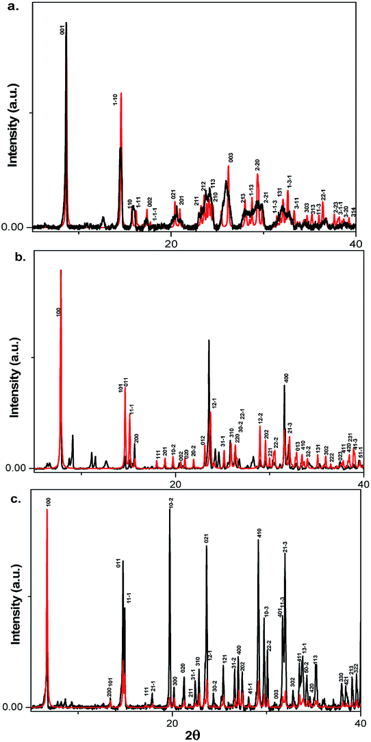 | ||
Fig. 1
 X-ray powder diffraction and X-ray powder diffraction and  calculated patterns from single crystal data of (a) BdAPbI4 (b) HdAPbI4 and (c) OdAPbI4. calculated patterns from single crystal data of (a) BdAPbI4 (b) HdAPbI4 and (c) OdAPbI4. | ||
Broad peaks can be noted in the diffractograms of BdAPbI4. The reason can most likely be attributed to disorder in the structure. Deviations in relative peak intensities noted between calculated and experimentally determined diffractograms are likely to be caused by crystal orientation bias in the powders studied. For instance, this effect refers to the (100) plane in all three materials. X-ray diffraction pattern of the material's thin film on TiO2 layer showed that for BdAPbI4 and HdAPbI4 films are representative of the bulk materials, while for OdAPbI4 some new peaks are recorded for the thin films materials on the TiO2. This mismatched pattern can be originated from the bigger unit cell volume for OdAPbI4 and the related interference for material crystallization on mesoporous TiO2 (see Fig. S6†). Spin coated MAPbI3 films from DMF solutions were investigated by powder X-ray diffraction and the diffractograms are presented in Fig. S7.† In accordance to the previous reports,24 PbI2 peaks were obtained indicating a small portion of PbI2 due to instability of MAPbI3 in the ambient atmosphere.
All three materials show very related two dimensional (2D) perovskite structures consisting of planes of corner-sharing octahedra of [PbI6] units separated by the organic cation (Fig. 2, 3, S1 and S2†). A representative structure of 2D BdAPbI4 is presented in Fig. S1,† 2D HdAPbI4 and 2D OdAPbI4 are depicted in Fig. 2 and S2,† respectively.
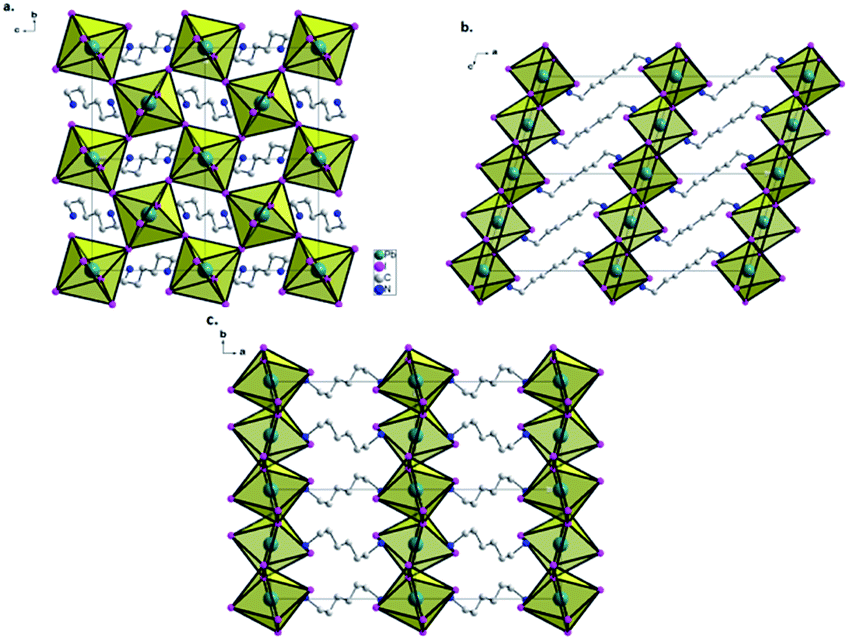 | ||
| Fig. 2 Structure of HdAPbI4 showed along the three crystallographic axes. | ||
 | ||
| Fig. 3 Structural planes of (a) BdAPbI4 (b) HdAPbI4 (c) OdAPbI4. | ||
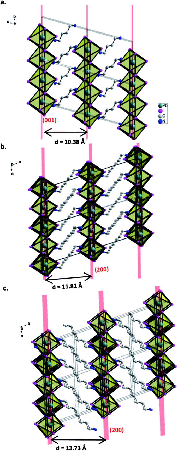
BdAPbI4 crystallizes in the triclinic system in the space group P1 and with the lattice parameters a = 8.4815(14) Å, b = 8.8472(14) Å, and c = 11.2028(17) Å.
Both HdAPbI4 and OdAPbI4 crystallize in the monoclinic system in the P21/c space group symmetry and in a slightly larger unit cell for OdAPbI4. The unit cell of HdAPbI4 is described by a = 11.8055(6) Å, b = 8.4509(4) Å, and c = 9.0262(5) Å, and for OdAPbI4 by a = 13.7343(10) Å, b = 8.3435(5) Å, and c = 9.0041(6) Å. More details of the crystallographic analyses are presented in Table 1. The organic cations are imbedded in the structure as a link between the lead iodide planes. Hence, the distance between the inorganic planes correlates with the size of the cation used. For BdAPbI4, the inorganic component of the structure is confined along the (001) planes connected by the BdA cations. The distance between the planes (defined as the distance between the Pb atoms in adjacent planes) is 10.4 Å. As could be expected, this distance is larger in HdAPbI4 and OdAPbI4 due to the larger organic cations present in the structures. The 2D perovskite planes in HdAPbI4 follow the (200) direction with a 11.8 Å interplane distance. This trend is extended by OdAPbI4 with an interplane Pb–Pb distance of 13.7 Å. The interlayer distances between iodide ions in two adjacent planes are 4.25 Å in BdAPbI4, 6.06 Å in HdAPbI4, and 8.29 Å in OdAPbI4.
| BdAPbI4 | HdAPbI4 | OdAPbI4 | MAPbI3 (ref. 19) | |
|---|---|---|---|---|
| Space group | P1 (1) (triclinic) | P21/c (monoclinic) | P21/c (monoclinic) |
Pm![[3 with combining macron]](https://www.rsc.org/images/entities/char_0033_0304.gif) m m |
| Cell lengths (Å) | a 8.4815(14) | a 11.8055(6) | a 13.7343(10) | a 6.284 |
| b 8.8472(14) | b 8.4509(4) | b 8.3435(5) | b 6.284 | |
| c 11.2028(17) | c 9.0262(5) | c 9.0041(6) | c 6.284 | |
| Cell angles | α = 76.83 (7) | α 90.00 | α 90.00 | α 90.00 |
| β = 69.67 (7) | β 107.073(2) | β 106.577(4) | β 90.00 | |
| γ = 89.46 (9) | γ 90.00 | γ 90.00 | γ 90.00 | |
| Cell volume (Å3) | 765.28 | 860.833 | 988.915 | 248.15 |
| Z | 4 | 4 | 4 | 1 |
The distances between two central Pb octahedral atoms inside a plane are 6.10, 6.19 and 6.14 Å for BdAPbI4, HdAPbI4 and OdAPbI4, respectively. These are comparable to the corresponding 6.28 Å distances found in MAPbI3. It is notable that the intraplane arrangement of the corner-sharing [PbI6] octahedra is considerably less ordered with Pb–I–Pb angles of 150°, 148° and 147° for BdAPbI4, HdAPbI4, and OdAPbI4, respectively, in contrast to the 180° angle found in the cubic MAPbI3 structure.19 More details are presented in Table S1† together with structural details of methylammonium lead iodide in Table 1.
The well-defined cation positions obtained from the crystallography in the 2D materials indicate that cation movement and migration must be considerably lower than in MAPbI3. The immobile cations will generate a permanent dipole moment throughout the material network rather than the rotating dipole moment in MAPbI3, which may affect the process of charge separation.20,21
Thermal analysis
The thermal stability of the new materials and examination of possible phase transitions were investigated using Differential Scanning Calorimetry (DSC). An impressive stability was observed for the materials up to at least 205 °C for BdAPbI4 and 210 °C for HdAPbI4 (Fig. S4 and S5†). No phase transition was observed up to these temperatures indicating high thermal stability for these materials in contrast to MAPbI3.Absorption spectroscopy
The optical properties of the materials were investigated by UV-visible characterization and the results are presented in Fig. 4. The strong absorption at longer wavelengths can be attributed to transitions over the band gap of the materials. Band gaps were estimated using the Tauc formula34 (Tauc plots are presented in Fig. S3†). The band edges emerge as 2.37 eV, 2.44 eV and 2.55 eV for BdAPbI4, HdAPbI4, and OdAPbI4, respectively. The increase in structural spacing between the inorganic planes in the materials can clearly be correlated to an increase in the band gaps. This may be related to quantum confinement reducing orbital overlap between the lead iodide structural planes and hence a shift of the band gap to higher energies. Although band edges are not very different, incorporation of a bigger cation drastically decrease the slope of the absorption edge, thus suggesting a trend in decreasing absorption coefficient. Previous studies have shown different optical properties for different crystal sizes of the 3D lead perovskites.35,36 Assuming a similar behavior for this class of 2D perovskites, due to the larger volume of the cation in OdAPbI4 the crystallinity of the material may be lower, leading to a lower absorption coefficient. The absorption edges observed correlate very well with the IPCE spectra of the resulting solar cells (see Fig. 6c).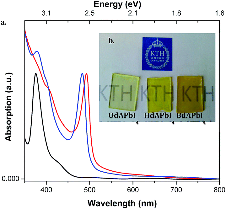 | ||
Fig. 4 (a) UV-visible absorption spectra of  BdAPbI4, BdAPbI4,  HdAPbI4, and HdAPbI4, and  OdAPbI4 on spin-coated mesoporous thin films of TiO2 (b) photographs of the materials. OdAPbI4 on spin-coated mesoporous thin films of TiO2 (b) photographs of the materials. | ||
Cyclic voltammetry and ultraviolet photoelectron spectroscopy (UPS)
The band energy diagram provides deeper insights into the charge transfer dynamics of the solar cells constructed based on the 2D perovskite materials (Fig. 5). Due to the high stability of these materials, valence band maxima were determined by cyclic voltammetry (CV). In addition Ultraviolet Photoelectron Spectroscopy (UPS) was used to confirm the CV results. Results from the two types of experiments match well (Table S9†). The UPS results suggest direct band gap behavior for the three materials. The CV results offer valence band positions at −5.33 eV, −5.56 eV, and −5.36 eV for BdAPbI4, HdAPbI4, and OdAPbI4, respectively.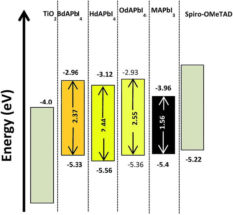 | ||
| Fig. 5 Band energy diagrams of the 2D perovskite materials compared to other components of the solar cells. | ||
It is notable that the position of the valence band edge energy does not change drastically (less than 0.16 eV) with respect to the structural changes from 3D to 2D (cf.MAPbI3). However the conduction band edge energy increases upon a decrease in dimensionality. This suggests that the comparatively low energy of the TiO2 conduction band may limit the obtained open circuit voltages from these materials.
For the 3D perovskite MAPbI3, previous studies have shown a large contribution from iodide p-orbitals to the valence band, while the conduction band mostly consists of contributions from the Pb p-orbital.37,38 The above results indicate that the composition of the valence bands in the new 2D materials should be similar to the 3D compound, but that the orbital composition of the conduction bands may differ.
Conductivity
Conductivities of the materials were obtained as 1.3 × 10⁻⁵ S cm−1, 1.3 × 10⁻⁵ S cm−1, and 1.3 × 10⁻⁵ S cm−1 for BdAPbI4, HdAPbI4, and OdAPbI4, respectively, where MAPbI3 was employed as a control in the measurements. The conductivities decrease one order of magnitude going from 3D to 2D structures. In our previous study,19 we showed that the conductivity is dependent on the dimensionality of the structure of the materials, where the conductivity of 3D MAPbI3 was 1.1 × 10⁻⁴ S cm−1, while a conductivity of 1.3 × 10⁻⁶ S cm−1 was recorded for the 1D (CH3CH2NH3)PbI3.Solar cells
Solid state solar cells were prepared based on the three new 2D materials as the light absorbing/charge transport component. Precursor solutions of the three 2D materials were spin-coated into TiO2 mesoporous films (Fig. 6a). Solar cells based on the MAPbI3 material were prepared under the same conditions for comparison (well aware of the fact the moist conditions will produce MAPbI3-based solar cells of quite poor quality). The better moisture resistance of the 2D materials was indeed a beneficial property in the production of robust and easy to handle solar cells. The best solar cells based on BdAPbI4 showed an efficiency of 1.08% with 2.9 mA cm−2 in current density. To the best of our knowledge, this represents the highest efficiency obtained from any pure 2D perovskite solar cell.31 Considering how much light is lost because of the relatively large band gap for the material (2.37 eV) and losses due to thermalization for electrons injected into TiO2, the results are rather impressive. For the solar cells based on BdAPbI4, HdAPbI4 and OdAPbI4, the open circuit voltages were 870 mV, 725 mV and 732 mV respectively. Lower voltages were obtained for some of the 2D based solar cells as compared to 805 mV obtained for the 3D MAPbI3 based solar cells. Substantial charge recombination losses in OdAPbI4 and HdAPbI4 solar cells likely reduced the difference in quasi-Fermi levels for TiO2 and Spiro-OMeTAD, decreasing the open-circuit voltage for these devices.39 The low performance of the MAPbI3 solar cells as compared to the previously published reports3 may be attributed to the poor stability of the MAPbI3 films under humid conditions.31 It is notable that the pure iodide methylammonium lead iodide perovskite solar cells were made by a one step process under ambient conditions, and the highest published efficiency for this type of solar cells is just over 9% (ref. 3) under controlled glove box condition. In our previous report, an efficiency of 7.4% was obtained for MAPbI3 at much lower humidity;19 this indicates a high dependence of MAPbI3 based solar cells to humidity. The current–voltage characterization details are presented in Table 2 and Fig. 4.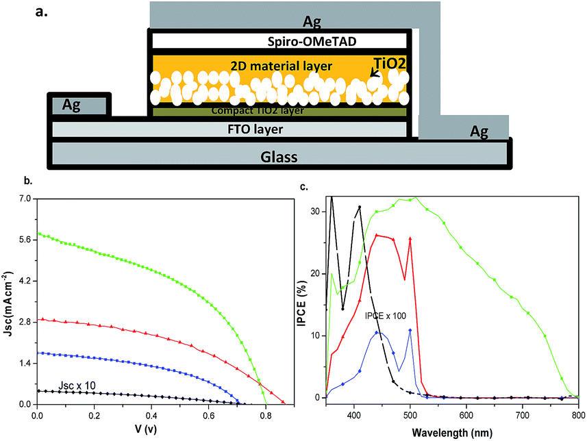 | ||
Fig. 6 (a) Schematic device architecture for the mesoporous solid state solar cells, (b) I–V and (c) IPCE curves of the solar cells based on  BdAPbI4, BdAPbI4,  HdAPbI4, HdAPbI4,  OdAPbI4, and OdAPbI4, and  MAPbI3. I–V characterizations were performed under 1 sun AM1.5G illumination. For ease of comparison the OdAPbI4 based solar cell results, the Jsc is multiplied by a factor of 10 and the IPCE is multiplied by a factor of 100. MAPbI3. I–V characterizations were performed under 1 sun AM1.5G illumination. For ease of comparison the OdAPbI4 based solar cell results, the Jsc is multiplied by a factor of 10 and the IPCE is multiplied by a factor of 100. | ||
| Eff (%) | V oc (V) | J sc (mA cm−2) | FF | APCE (%) | Band gap (eV) | Conductivity (S cm−1) | |
|---|---|---|---|---|---|---|---|
| BdAPbI4 | 1.082 | 0.870 | 2.894 | 0.430 | 24.2 | 2.37 | 1.3 × 10⁻⁵ |
| HdAPbI4 | 0.592 | 0.725 | 1.735 | 0.471 | 8.1 | 2.44 | 1.2 × 10⁻⁵ |
| OdAPbI4 | 0.012 | 0.732 | 0.047 | 0.340 | 0.23 | 2.55 | 1.2 × 10⁻⁵ |
| MAPbI3 | 2.117 | 0.805 | 5.858 | 0.449 | 31.2 | 1.56 (ref. 19) | 1.3 × 10⁻⁴ |
Due to the differences in recombination loss and in light absorption efficiencies there is no simple correlation between the band gap of the 2D materials and the resulting open circuit voltage recorded from the corresponding solar cells. Incident photon-to-current conversion efficiencies (IPCE)s are presented in Fig. 6c. These curves are in good agreement with the absorption spectra and estimated band gaps. For sake of simplicity the effect of light harvesting efficiency can be omitted from the IPCE data resulting in absorbed photon-to-current conversion efficiency (APCE). APCEs for the solar cells based on BdAPbI4 were 24.2%, substantially lower than the 31.2% obtained for cells based on MAPbI3. This trend in APCE resulted in 8.1% and 0.23% for cells based on HdAPbI4 and OdAPbI4, respectively. The general conclusion is that the bulkier cation the less suitable 2D perovskite material for solar cell applications. Very poor photovoltaic performance was obtained for solar cells based on OdAPbI4, although this material shows similar electrical conductivity as and a slightly larger band gap than the other 2D materials. Most likely this can be linked to the relatively large interplane distances not being compatible with the small pore size in the mesoporous TiO2 substrate.
Relating the IPCE values to conductivity, we can estimate that conductivity between structural planes for the three related perovskites follows BdAPbI4 > HdAPbI4 ≫ OdAPbI4. These findings suggest that charge-injection or charge-collection efficiency is a determining factor for the difference in the solar cell performance observed. The CV and UPS data indicate that both electron injection or hole injection are energetically favorable, which suggests that charge recombination may limit charge collection in solar cells that incorporate these materials.
The I–V-characterizations were performed at 10 mV s−1 to reduce hysteresis effect,40 but a small hysteresis has been observed for the 2D-based solar cells. Ion migration is suggested as one of the origins for the hysteresis in the perovskite solar cells.20 Since in these 2D perovskite the cations are well-defined by X-ray single crystallography, it can be suggested that this portion of hysteresis is much lower in these 2D based perovskite solar cells compare to MAPbI3 solar cells (see Fig. S8 and Table S11†).
I–V measurements of the solar cells were repeated after 48 and 96 hours (see Table S9†). For BdAPbI4 and HdAPbI4, the solar cells efficiency drops from 1.082% to 0.798% and from 0.592% to 0.339% after 4 days respectively, while for MAPbI3 the efficiency was reduced from 2.11% to 0.03% over that same period. This is further evidence for the increased stability of the 2D perovskite solar cells in comparison to MAPbI3 solar cells under ambient conditions.
Previous attempts at producing low dimensional lead(II) halide solar cells resulted in materials with low conductivity and a non-perovskite structure.19 Here, we attribute the increased efficiency of solar cells with diammonium cations to the decreased distance between lead(II) halide planes and the rigid dication. For comparison, the molecular volume of two ethylammonium cations (CH3CH2NH3)+ is similar to that of one butyldiammonium cation, [NH3(CH2)4NH3]2+; however, the dication has fewer rotational degrees of freedom than would be obtained for two monocations. The dications form more crystalline materials with higher conductivities, because they have fewer degrees of freedom during crystallization and in the fully formed materials.
Methylammonium lead iodide has been used as top layer in tandem cells.41,42 Although representing a novel idea, methylammonium lead iodide with a 1.5 eV band gap is not an optimal choice for harvesting high energy photons. For instance for an ideal tandem cell incorporating silicon with a band gap of 1.1 eV, a top layer of a perovskite with a 1.8 eV band gap is required to render a 42% theoretical efficiency.43 The present 2D perovskite materials with 2.3–2.5 eV band gaps are highly appropriate to combine with CdTe (1.5 eV) to reach a 35% theoretical efficiency.43 Energy diagrams show a better coupling capability of the 2D materials for tandem devices than MAPbI3. There is sufficient driving force between the solar cell components suggesting no problems in association with charge injection for such solar cells. In addition the higher energies of the conduction bands in these materials in combination with their higher stability may make them suitable candidates for reductive photoelectrochemical studies or photocatalysis.
Conclusions
We have synthesized and characterized three new 2D alkyl diammonium lead iodide materials. Detailed structural information of these materials has been reported based on single crystal X-ray diffraction. Diammonium cations incorporated in to the structures of these materials serve as a bridge between the inorganic lead iodide planes. Powder diffraction patterns of the bulk materials match single crystal data quite well, which indicates that the single crystal structures of the materials are representative for the bulk. UV-visible absorption spectra of the materials render optical properties and band gaps of 2.37 eV, 2.44 eV and 2.55 eV for BdAPbI4, HdAPbI4 and OdAPbI4, respectively. Energy band diagrams of the materials were obtained from cyclic voltammetry and from ultraviolet photoelectron spectroscopy giving complementary information. Thermal stability was recorded for BdAPbI4 and HdAPbI4 in excess of 200 °C. Solar cells based on the 2D perovskite material BdAPbI4 had a power conversion efficiency of 1.082%, as compared to 2.1% for MAPbI3 based solar cells manufactured under the same (humid) conditions. The current study has offered insights into the effects of structural dimensionality on physical properties as well as their applicability in solar cells. In further work, we will focus on optimization of the structural networks in lead-free materials for photovoltaic applications.Acknowledgements
This work was supported by Swedish Government through “STandUP for ENERGY”, The Swedish Energy Agency, The Swedish Research Council, Knut & Alice Wallenberg Foundation, and the Korea-Sweden Collaborative Research Program through the National Research Foundation of Korea (NRF) funded by the Ministry of Science, ICT and Future Planning (NRF-2014K1A3A1A47067328).References
- A. Kojima, K. Teshima, Y. Shirai and T. Miyasaka, J. Am. Chem. Soc., 2009, 131, 6050–6051 CrossRef CAS PubMed.
- J.-H. Im, C.-R. Lee, J.-W. Lee, S.-W. Park and N.-G. Park, Nanoscale, 2011, 3, 4088–4093 RSC.
- H.-S. Kim, C.-R. Lee, J.-H. Im, K.-B. Lee, T. Moehl, A. Marchioro, S.-J. Moon, R. Humphry-Baker, J.-H. Yum, J. E. Moser, M. Gratzel and N.-G. Park, Sci. Rep., 2012, 2, 591 Search PubMed.
- M. M. Lee, J. Teuscher, T. Miyasaka, T. N. Murakami and H. J. Snaith, Science, 2012, 338, 643–647 CrossRef CAS PubMed.
- J. Burschka, N. Pellet, S.-J. Moon, R. Humphry-Baker, P. Gao, M. K. Nazeeruddin and M. Gratzel, Nature, 2013, 499, 316–319 CrossRef CAS PubMed.
- M. Liu, M. B. Johnston and H. J. Snaith, Nature, 2013, 501, 395–398 CrossRef CAS PubMed.
- W. S. Yang, J. H. Noh, N. J. Jeon, Y. C. Kim, S. Ryu, J. Seo and S. I. Seok, Science, 2015, 348, 1234–1237 CrossRef CAS PubMed.
- D. Bi, W. Tress, M. I. Dar, P. Gao, J. Luo, C. Renevier, K. Schenk, A. Abate, F. Giordano, J.-P. Correa Baena, J.-D. Decoppet, S. M. Zakeeruddin, M. K. Nazeeruddin, M. Grätzel and A. Hagfeldt, Sci. Adv., 2016, 2(1), e1501170 Search PubMed.
- http://www.nrel.gov/ncpv/images/efficiency_chart.jpg .
- N. J. Jeon, J. H. Noh, Y. C. Kim, W. S. Yang, S. Ryu and S. I. Seok, Nat. Mater., 2014, 13, 897–903 CrossRef CAS PubMed.
- L. N. Quan, M. Yuan, R. Comin, O. Voznyy, E. M. Beauregard, S. Hoogland, A. Buin, A. R. Kirmani, K. Zhao, A. Amassian, D. H. Kim and E. H. Sargent, J. Am. Chem. Soc., 2016, 138, 2649–2655 CrossRef CAS PubMed.
- A. Poglitsch and D. Weber, J. Chem. Phys., 1987, 87, 6373–6378 CrossRef CAS.
- F. Somma, K. Nitsch, C. Giampaolo, A. R. Phani and S. Santucci, Superficies Vacio, 1999, 9, 3 Search PubMed.
- I. Chung, J.-H. Song, J. Im, J. Androulakis, C. D. Malliakas, H. Li, A. J. Freeman, J. T. Kenney and M. G. Kanatzidis, J. Am. Chem. Soc., 2012, 134, 8579–8587 CrossRef CAS PubMed.
- C. C. Stoumpos, C. D. Malliakas and M. G. Kanatzidis, Inorg. Chem., 2013, 52, 9019–9038 CrossRef CAS PubMed.
- C. C. Stoumpos, L. Frazer, D. J. Clark, Y. S. Kim, S. H. Rhim, A. J. Freeman, J. B. Ketterson, J. I. Jang and M. G. Kanatzidis, J. Am. Chem. Soc., 2015, 137, 6804–6819 CrossRef CAS PubMed.
- D. B. Mitzi, C. A. Feild, Z. Schlesinger and R. B. Laibowitz, J. Solid State Chem., 1995, 114, 159–163 CrossRef CAS.
- T. Baikie, Y. Fang, J. M. Kadro, M. Schreyer, F. Wei, S. G. Mhaisalkar, M. Graetzel and T. J. White, J. Mater. Chem. A, 2013, 1, 5628–5641 CAS.
- M. Safdari, A. Fischer, B. Xu, L. Kloo and J. M. Gardner, J. Mater. Chem. A, 2015, 3, 9201–9207 CAS.
- J. M. Azpiroz, E. Mosconi, J. Bisquert and F. De Angelis, Energy Environ. Sci., 2015, 8, 2118–2127 CAS.
- C. Eames, J. M. Frost, P. R. F. Barnes, B. C. O'Regan, A. Walsh and M. S. Islam, Nat. Commun., 2015, 6, 7497 CrossRef CAS PubMed.
- V. D'Innocenzo, G. Grancini, M. J. P. Alcocer, A. R. S. Kandada, S. D. Stranks, M. M. Lee, G. Lanzani, H. J. Snaith and A. Petrozza, Nat. Commun., 2014, 5, 3586 Search PubMed.
- K. Galkowski, A. Mitioglu, A. Miyata, P. Plochocka, O. Portugall, G. E. Eperon, J. T.-W. Wang, T. Stergiopoulos, S. D. Stranks, H. J. Snaith and R. J. Nicholas, Energy Environ. Sci., 2016, 9, 962–970 CAS.
- S. Pathak, A. Sepe, A. Sadhanala, F. Deschler, A. Haghighirad, N. Sakai, K. C. Goedel, S. D. Stranks, N. Noel, M. Price, S. Hüttner, N. A. Hawkins, R. H. Friend, U. Steiner and H. J. Snaith, ACS Nano, 2015, 9, 2311–2320 CrossRef CAS PubMed.
- J. Yang, B. D. Siempelkamp, E. Mosconi, F. De Angelis and T. L. Kelly, Chem. Mater., 2015, 27, 4229–4236 CrossRef CAS.
- R. K. Misra, S. Aharon, B. Li, D. Mogilyansky, I. Visoly-Fisher, L. Etgar and E. A. Katz, J. Phys. Chem. Lett., 2015, 6, 326–330 CrossRef CAS PubMed.
- T. M. Koh, K. Fu, Y. Fang, S. Chen, T. C. Sum, N. Mathews, S. G. Mhaisalkar, P. P. Boix and T. Baikie, J. Phys. Chem. C, 2014, 118, 16458–16462 CAS.
- D. B. Mitzi, K. Chondroudis and C. R. Kagan, Inorg. Chem., 1999, 38, 6246–6256 CrossRef CAS PubMed.
- D. B. Mitzi, Inorg. Chem., 2000, 39, 6107–6113 CrossRef CAS PubMed.
- K. Liang, D. B. Mitzi and M. T. Prikas, Chem. Mater., 1998, 10, 403–411 CrossRef CAS.
- D. H. Cao, C. C. Stoumpos, O. K. Farha, J. T. Hupp and M. G. Kanatzidis, J. Am. Chem. Soc., 2015, 137, 7843–7850 CrossRef CAS PubMed.
- I. C. Smith, E. T. Hoke, D. Solis-Ibarra, M. D. McGehee and H. I. Karunadasa, Angew. Chem., Int. Ed., 2014, 53, 11232–11235 CrossRef CAS PubMed.
- B. A. B. S. Apex II, 2013.2–0, Bruker AXS Inc., Madison, WI, USA, 2013 Search PubMed.
- J. Tauc, R. Grigorovici and A. Vancu, Phys. Status Solidi B, 1996, 15, 10 Search PubMed.
- M. De Bastiani, V. D'Innocenzo, S. D. Stranks, H. J. Snaith and A. Petrozza, APL Mater., 2014, 2, 081509 CrossRef.
- W. Zhang, M. Saliba, D. T. Moore, S. K. Pathak, M. T. Hörantner, T. Stergiopoulos, S. D. Stranks, G. E. Eperon, J. A. Alexander-Webber, A. Abate, A. Sadhanala, S. Yao, Y. Chen, R. H. Friend, L. A. Estroff, U. Wiesner and H. J. Snaith, Nat. Commun., 2015, 6, 6142 CrossRef CAS PubMed.
- T. Umebayashi, K. Asai, T. Kondo and A. Nakao, Phys. Rev. B: Condens. Matter Mater. Phys., 2003, 67, 155405 CrossRef.
- R. Lindblad, D. Bi, B.-w. Park, J. Oscarsson, M. Gorgoi, H. Siegbahn, M. Odelius, E. M. J. Johansson and H. Rensmo, J. Phys. Chem. Lett., 2014, 5, 648–653 CrossRef CAS PubMed.
- E. A. Muljarov, S. G. Tikhodeev, N. A. Gippius and T. Ishihara, Phys. Rev. B: Condens. Matter Mater. Phys., 1995, 51, 14370–14378 CrossRef CAS.
- E. L. Unger, E. T. Hoke, C. D. Bailie, W. H. Nguyen, A. R. Bowring, T. Heumuller, M. G. Christoforo and M. D. McGehee, Energy Environ. Sci., 2014, 7, 3690–3698 CAS.
- C. D. Bailie, M. G. Christoforo, J. P. Mailoa, A. R. Bowring, E. L. Unger, W. H. Nguyen, J. Burschka, N. Pellet, J. Z. Lee, M. Gratzel, R. Noufi, T. Buonassisi, A. Salleo and M. D. McGehee, Energy Environ. Sci., 2015, 8, 956–963 CAS.
- P. Loper, S.-J. Moon, S. Martin de Nicolas, B. Niesen, M. Ledinsky, S. Nicolay, J. Bailat, J.-H. Yum, S. De Wolf and C. Ballif, Phys. Chem. Chem. Phys., 2015, 17, 1619–1629 RSC.
- A. D. Vos, J. Phys. D: Appl. Phys., 1980, 13, 839 CrossRef.
Footnote |
| † Electronic supplementary information (ESI) available: Tables S1–S4 including atomic parameters of the structure of the three new materials, Fig. S1 and S2, two 2D structures of butyl 1,4-diammonium lead iodide and octyl 1,8-diammonium lead iodide along the three crystallographic axes. Tables S5–S11 and Fig. S3–S9 describe structural and photochemical characterization. CIF files for the structures are available at the Cambridge Crystallographic Data Center (CCDC) referring to the deposition numbers 1420433 and 1420434 for HdAPbI4 and OdAPbI4, respectively. See DOI: 10.1039/c6ta05055g |
| This journal is © The Royal Society of Chemistry 2016 |