
 Open Access Article
 This Open Access Article is licensed under a Creative Commons Attribution-Non Commercial 3.0 Unported Licence
Optical analysis of CH3NH3SnxPb1−xI3 absorbers: a roadmap for perovskite-on-perovskite tandem solar cells†
Miguel
Anaya‡
a,
Juan P.
Correa-Baena‡
*b,
Gabriel
Lozano
a,
Michael
Saliba
c,
Pablo
Anguita
a,
Bart
Roose
d,
Antonio
Abate
c,
Ullrich
Steiner
 d,
Michael
Grätzel
c,
Mauricio E.
Calvo
a,
Anders
Hagfeldt
b and
Hernán
Míguez
*a
d,
Michael
Grätzel
c,
Mauricio E.
Calvo
a,
Anders
Hagfeldt
b and
Hernán
Míguez
*a
aInstitute of Materials Science of Seville, Spanish National Research Council-University of Seville, Américo Vespucio 49, 41092, Seville, Spain. E-mail: h.miguez@csic.es
bLaboratory for Photomolecular Science, Institute of Chemical Sciences and Engineering, Ecole Polytechnique Fédérale de Lausanne, CH-1015-Lausanne, Switzerland. E-mail: juan.correa@epfl.ch
cLaboratory for Photonics and Interfaces, Institute of Chemical Sciences and Engineering, Ecole Polytechnique Fédérale de Lausanne, CH-1015-Lausanne, Switzerland
dAdolphe Merkle Institute, Chemin des Verdiers 4, CH-1700 Fribourg, Switzerland
First published on 29th June 2016
Abstract
Organic–inorganic perovskite structures in which lead is substituted by tin are exceptional candidates for broadband light absorption. Herein we present a thorough analysis of the optical properties of CH3NH3SnxPb1−xI3 films, providing the field with definitive insights about the possibilities of these materials for perovskite solar cells of superior efficiency. We report a user's guide based on the first set of optical constants obtained for a series of tin/lead perovskite films, which was only possible to measure due to the preparation of optical quality thin layers. According to the Shockley–Queisser theory, CH3NH3SnxPb1−xI3 compounds promise a substantial enhancement of both short circuit photocurrent and power conversion efficiency in single junction solar cells. Moreover, we propose a novel tandem architecture design in which both top and bottom cells are made of perovskite absorbers. Our calculations indicate that such perovskite-on-perovskite tandem devices could reach efficiencies over 35%. Our analysis serves to establish the first roadmap for this type of cells based on actual optical characterization data. We foresee that this study will encourage the research on novel near-infrared perovskite materials for photovoltaic applications, which may have implications in the rapidly emerging field of tandem devices.
In the last few years methylammonium lead iodide, a well-known compound with a perovskite crystal structure1–3 has come into light as a unique material for solar power and optoelectronic applications.4–7 Indeed, CH3NH3PbI3 and alternative APbX3 perovskites yield unprecedented results in solar energy conversion devices8–12 due to their large extinction coefficient, low exciton binding energy, and large charge diffusion length.13,14 Since the performance of standard lead-based perovskite devices is reaching the theoretical limit,15,16 nowadays, most research efforts pursue to unravel the electrical and photophysical properties of perovskite materials,13,17,18 in order to achieve devices with stabilised efficiencies,19–21 and long-term durability.22–24
A promising but scarcely explored route to achieve further efficient devices consists in the development of novel perovskite light harvesters.25 In particular, those in which lead is substituted by other metals,26 especially tin, give rise to narrower bandgap energies, which results in a better harnessing of the incident sunlight.27–35 However, limited film quality and fast oxidation of Sn2+ to Sn4+, which induces self-doping that turns the semiconducting perovskite into a conducting one,36 hamper the power conversion efficiencies (PCEs) of actual devices that never surpass few percents.28–35 Nevertheless, the interest in them is still enormous, as this particular type of perovskite is the only one that permits extending the bandgap to the near-infrared (NIR) and hence reaching the Shockley–Queisser (SQ) limit. A widely explored route to surpass the SQ limit consists of the combination of two or more single junction devices into a tandem system to harvest a larger fraction of the sunlight. So far, efforts are intensifying to demonstrate double-junction devices in which APbX3 perovskites and CIGS or Si materials are employed as top and bottom cells, respectively.37–40 Alternatively, tin–lead perovskites of tuneable bandgap offer a complete new range of possibilities to develop solution processed absorbers to be integrated into devices with tandem configuration of higher efficiency. However, a thorough analysis on the implications of such tin–lead perovskites for photovoltaic applications is still missing.
In this paper we employ a novel synthesis and deposition route to obtain smooth and pinhole-free CH3NH3SnxPb1−xI3 films with high optical quality by solution processed techniques. This allows performing an in-depth optical characterization of the films, and extracting, for the first time, the complex refractive index of the different perovskite compositions based on the Sn/Pb alloys. We use a rigorous theoretical model, based on the transfer matrix formalism,41 to predict the optical behaviour of a solar device integrating these materials and to estimate the maximum short circuit photocurrent (Jsc) values expected for each Sn/Pb ratio. The combination of bandgap engineering and high optical quality achieved allow us to propose a perovskite-on-perovskite tandem solar cell architecture in which CH3NH3PbI3 and CH3NH3Sn0.85Pb0.15I3 perovskite films are employed as active layers for the top and bottom cell, respectively. This design promises to be of great importance for the immediate future of this rapidly growing field.
Perovskite materials with changing Sn and Pb compositions in CH3NH3SnxPb1−xI3, where x is varied from 0 to 1 (otherwise denoted throughout the text as 0% and 100%, respectively), are prepared by taking different volumes of two stock solutions of Pb and Sn perovskite precursors. Although full details are provided in the Methods section, it is worth mentioning that optical quality films were only obtained by means of a combination of precursor solvent engineering and anti-solvent deposition method, which induces fast crystallization of the mixed perovskite. Fig. 1a–c show the cross-sectional SEM images of the perovskite films with 0%, 50% and 100% content of Sn. Our synthesis route drives to layers that present smooth thickness variations, which are small enough to consider the perovskite–air interface plane-parallel for the impinging light. From top view SEM images (see Fig. 1d–f), it can be observed that crystalline grains are densely packed forming continuous films atop the mesoporous TiO2 layer, presenting no degradation at room temperature (see Fig. S1†). The crystal structures of compositions varying from 0% to 100% Sn were analysed by XRD (Fig. 1g). The gradual shift of the two dominant peaks appearing in all the composites, 2θ = 14° and 28.5°, is monitored as seen in Fig. 1h and i. This phenomenon has been shown by Hao et al., where the transition from the tetragonal to the cubic phase is explained by the distortion of the relative positions of the octahedra due to the randomly occupied Sn or Pb.32,34,42 Our deposition method induces the formation of large crystals, key for improving charge carrier transport in PSCs and yielding optimal photovoltaic performance in pure Pb perovskite solar cells.15,43
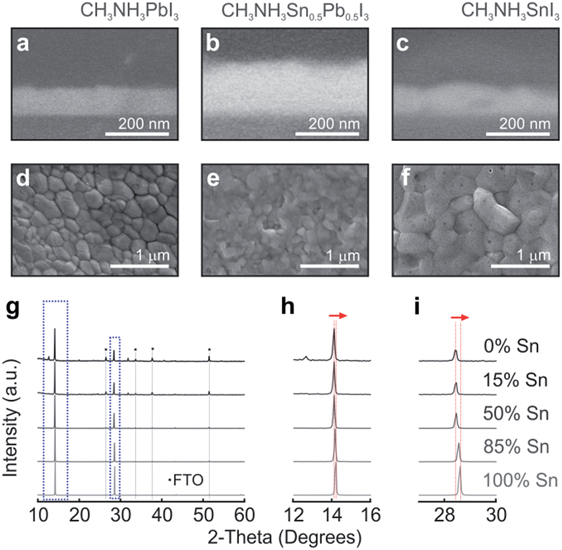 | ||
| Fig. 1 Cross-sectional (a–c) and top view (d–f) SEM images of the perovskite materials with different compositions as deposited on a glass substrate for optical analysis. Perovskite layers have been shaded with colours for the sake of clarity. (g) XRD diagrams corresponding to films in which the Sn/Pb ratio is gradually varied. Details of the 14° (h) and 28.5° (i) diffraction peaks. | ||
The pin-hole free, dense and planar character of the films prepared, which is preserved with time (see Fig. S1 and S2 of the ESI†), allows us to conduct a thorough study on the optical properties of perovskite films with different metal compositions, e.g. CH3NH3PbI3, CH3NH3Sn0.15Pb0.85I3, CH3NH3Sn0.5Pb0.5I3, CH3NH3Sn0.85Pb0.15I3 and CH3NH3SnI3. Our spectroscopic analysis reveals the high optical quality of the perovskite films, which do not suffer from the effect of diffuse scattering (see Fig. S3 of the ESI†). Absorptance measurements of the metal based mixed perovskite films are displayed in Fig. S4,† indicating a bandgap evolution already discussed elsewhere.44 The small fraction of the incident light absorbed at wavelengths larger than the bandgap discards the existence of intraband states, demonstrating the low density of defects present in the fabricated films.
Our optical measurements enable the analysis of the gradual change of the optical constants of the composites as the amount of tin increases at the expense of lead. Kramers–Kronig consistent real and imaginary parts of the complex refractive index of perovskite thin films with different compositions are displayed in Fig. 2a–e (see Fig. S5 of the ESI† for the complex dielectric permittivity). All fitting parameters can be found in Table S1 of the ESI.† The perovskite materials under analysis feature complex refractive indexes of similar order of magnitude regardless of the specific perovskite composition, implying that the Sn/Pb composites should be as efficient light harvesters as the standard Pb based perovskite. Fair agreement between theory (dashed lines) and experiment (solid lines) is found for the reflectance and transmittance spectra obtained for the different Sn/Pb perovskites, as displayed in Fig. 2f–j.
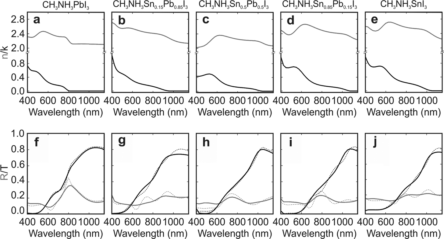 | ||
| Fig. 2 (a–e) Real (grey) and imaginary (black) parts of the complex refractive index of the mixed metal perovskite structures herein studied. (f–j) Experimental (dashed) and calculated (solid) spectra of the reflectance (grey) and transmittance (black) corresponding to the different films. | ||
The possibility to tune the bandgap of CH3NH3SnxPb1−xI3, from 1.60 eV for x = 0 to 1.17 eV for x = 0.85 (see Fig. 3a), brings the opportunity to develop the ideal absorber to maximize solar conversion efficiency. Fig. 3b displays the maximum theoretical Jsc and PCE that may be achieved as a function of the electronic energy gap (Eg) of the active material according to the SQ theory (see Methods section).45 As it is well known, the ideal Jsc increases as the Eg is reduced since a larger fraction of the incident sunlight is harvested by the absorbing material. In contrast, charge recombination increases with the reduction of Eg. As a consequence, a limiting PCE over 33% could be attained for Eg = 1.14 eV or Eg = 1.34 eV, considering an idealized system without additional losses, such as parasitic absorption or non-radiative recombination.
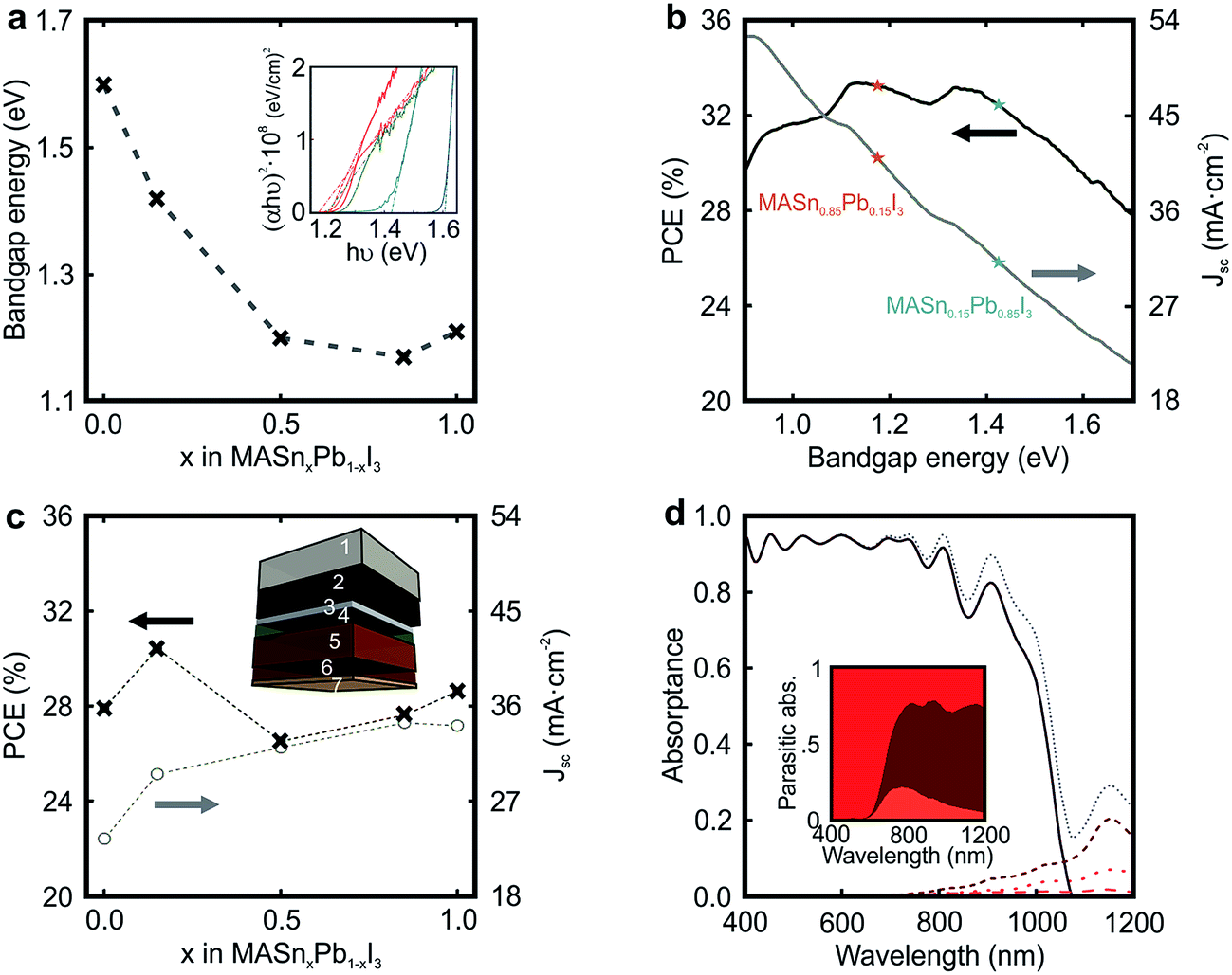 | ||
| Fig. 3 (a) Bandgap energy of the different mixed metal perovskite compositions versus the amount of Sn in the structure. The dashed grey line is only a guide for the eye. Inset shows the Tauc plots employed to estimate the direct bandgap energy. (b) Ideal calculated short circuit photocurrent (Jsc) and power conversion efficiency (PCE) as a function of the bandgap energy according to the Shockley–Queisser theory. (c) Calculated Jsc and PCE for simulated devices in which the percentage of Sn is increased at the expense of Pb. Inset shows the architecture of the simulated device: 1 mm of glass substrate (1), 650 nm of FTO layer (2), 50 nm of TiO2 compact layer (3), 85 nm of 50% porous TiO2 scaffold fully infiltrated by perovskite (4), 600 nm of perovskite capping layer (5), 240 nm of spiro-OMeTAD (6), and 50 nm of gold contact (7). (d) Spectral dependence of the fraction of light absorbed by the different layers comprising the cell: FTO (red dotted line), CH3NH3Sn0.85Pb0.15I3-based perovskite (black solid line), spiro-OMeTAD (brown short dashed line), and gold contact (orange dashed line). Inset shows details of the spectral dependence of the parasitic absorption in the FTO, spiro-OMeTAD and gold. | ||
In order to evaluate the impact of the integration of CH3NH3SnxPb1−xI3 films in actual solar cells, we introduce their optical constants in a model previously used to describe the performance of PSCs.41 The optical constants of the materials employed to model the cell are available in Fig. S6 of the ESI.† By this means, we can estimate the fraction of incident sunlight absorbed by the perovskite in a standard cell, whose scheme is represented in the inset of Fig. 3c. We assume a 600 nm perovskite capping layer, as this value has been demonstrated to yield state of the art efficiencies in pure Pb-based devices.15 In Fig. 3c, we present the calculated Jsc for devices in which the Sn/Pb ratio is varied. See Fig. S7 of the ESI† for a detailed analysis on the influence of the capping layer thickness. Our model considers (i) parasitic losses associated with the different absorbing materials present in the cell (FTO, spiro-OMeTAD or gold), (ii) reflection losses at the entrance of the cell, and (iii) ideal charge transport and charge collection, which implies that the internal quantum efficiency equals the light harvesting efficiency (IQE(λ) = LHE(λ)). It can be observed that the maximum Jsc follows the evolution of Eg (see Fig. 3a), i.e. perovskites with lower bandgaps should give rise to higher photo-generated currents. In particular, for an ideal PSC in which CH3NH3Sn0.85Pb0.15I3 is used as the light harvester, a Jsc of 34 mA cm−2 is foreseen. Fig. 3c also displays the maximum PCE achievable for each Sn/Pb perovskite composition. Notice that Jsc measured from state-of-the-art pure lead devices is nearly ideal.15 However, record devices feature PCEs that do not meet the values estimated according to the SQ theory, i.e. PCE of 22.1% vs. 27.9%.16 In order to provide a more realistic estimation of the efficiency of the PSC, it would be necessary to consider a thorough model of its electrical behaviour, which is out of the scope of this study. Our analysis indicates that a relative PCE enhancement of ∼10% with respect to the standard Pb perovskite material may be attained just by substituting 15% Pb by Sn in the perovskite film precursor (PCE of 27.9% vs. 30.4%), due to a 25% increase in the Jsc (23.5 mA cm−2vs. 29.5 mA cm−2) together with a more favorable Eg. In contrast, our estimations performed using a real device architecture indicate that the film with 85% Sn content (Eg = 1.17 eV) would give rise to a PCE far from that predicted for the ideal one according to the SQ theory (PCE of 28% vs. 33% expected). In order to explain the origin of this behaviour, in Fig. 3d we plot the fraction of light that the different components of the CH3NH3Sn0.85Pb0.15I3-based PSC absorb. It can be observed that the ratio between parasitic absorption, caused by optical losses occurring in spiro-OMeTAD and FTO, and productive absorption increases significantly in the NIR spectral range as the bandgap of the perovskite is gradually reduced, which results in a Jsc that is far from the ideal according to the Shockley–Queisser theory (Jsc of 34 mA cm−2vs. 41 mA cm−2 expected). In view of this result, it might be helpful, in order to minimize optical losses, to engineer novel hole transporting materials for cells operating in the NIR.
In order to prove the trends in photocurrent predicted by our optical model, we prepared devices of CH3NH3PbI3 and CH3NH3Sn0.15Pb0.85I3 perovskites. Full details are provided in the ESI: see Fig. S8 and S9.† Our experimental results indicate a substantial enhancement of the Jsc with respect to the standard Pb device, Jsc increasing from 19.5 mA cm−2 in the pure lead device to 24.8 mA cm−2 in the hybrid one, in fair agreement with our estimations. Despite the remarkable photocurrents attained, among the largest ever demonstrated for a perovskite material, and the relatively high voltages, comparable to those reported elsewhere,30 the performance of the Sn/Pb device is still modest due to the rather low fill factors (see Fig. S8 of the ESI†). Although the potential of Sn/Pb perovskite materials for solar cells seems undeniable, severe limitations of their chemical stability have prevented the observation of efficiencies close to the values herein predicted. A precise control of the oxygen exposure has proven to be critical to avoid the self-doping behaviour of Sn, which even in small quantities may be detrimental to achieve the expected performance. Oxygen levels as low as few parts per million can cause the oxidation of the Sn-based perovskite grains, which induces Sn4+ states which in turn increase charge carrier concentration. This translates into a degenerate semiconductor with metallic behaviour, inducing recombination centres, which has hampered so far the realization of efficient devices.36 Nevertheless, our measurements reveal the potential of Sn/Pb perovskite materials as light harvesters and open up a myriad of possibilities for optimization.
One of the most appealing properties of CH3NH3SnxPb1−xI3 perovskites is their narrow bandgap (1.17 < Eg < 1.60 eV) that opens the door to the realization of double-junction devices in which both top and bottom cells are based on perovskite absorbers. Indeed, a two-terminal monolithic architecture can be considered as a series circuit in which the current through the top and bottom cells is the same, and the voltage across the device is the sum of the voltages across each of the constituent cells. In order to optimize the performance of a tandem device, it is of utmost importance to find the configuration that gives rise to a similar fraction of the incident light harvested by the top and bottom cells: the so-called current-matching condition. We now want to provide the reader with a roadmap for the realistic design of perovskite-on-perovskite tandem devices. Although one precedent has been reported dealing with the combination of wide bandgap perovskites in order to achieve higher voltages,46 herein we propose a new architecture that, while providing a large voltage, is able to harvest a larger fraction of the incident light. As displayed in the inset of Fig. 4a, we consider a tandem solar cell with a planar configuration (see Fig. S10 of the ESI† for results concerning a mesostructured configuration). The active material chosen for the top cell is the standard CH3NH3PbI3 perovskite, which absorbs the incident light very efficiently up to 800 nm. Less energetic photons pass through the system and reach the CH3NH3Sn0.85Pb0.15I3 perovskite in the bottom cell, which harvests light up to ca. 1100 nm. Combined in a double-junction solar cell, the energy bandgaps (Eg = 1.6 eV and Eg = 1.17 eV) of these two materials are nearly optimized according to the SQ theory, similar to what occurs in CH3NH3PbI3/silicon tandem devices.37,38,40 SnO2 films are considered to act as electron selective layers that could be deposited by atomic layer deposition, for instance, for conformal low temperature deposition. This processing step is crucial, as it guarantees a proper band alignment of the perovskite materials with this electron selective layer, with the additional advantage of low temperature processing needed when dealing with perovskite materials.38,47
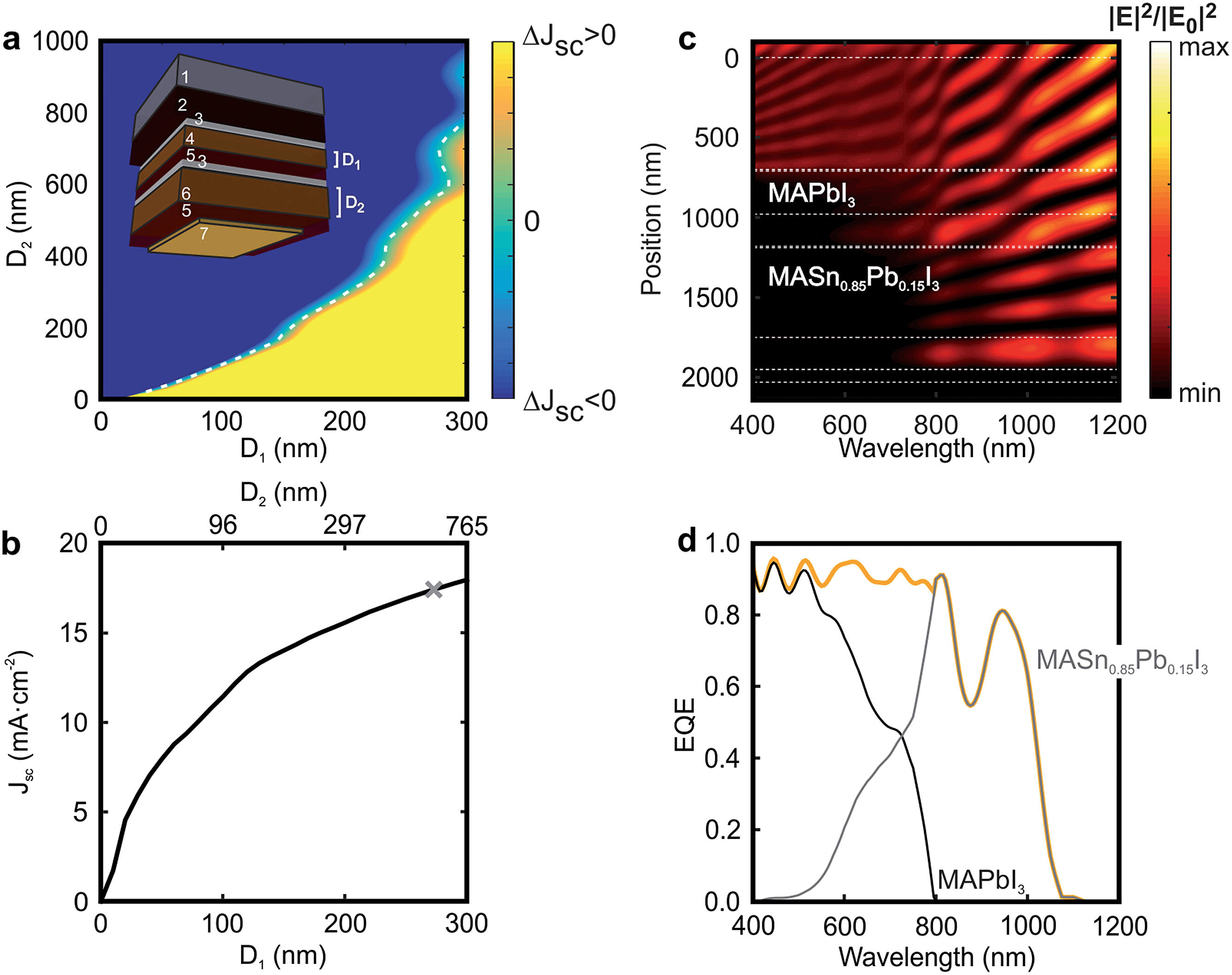 | ||
| Fig. 4 (a) Difference between short circuit currents extracted from the top and bottom cells composing a tandem device in which the CH3NH3PbI3 (D1) and CH3NH3Sn0.85Pb0.15I3 (D2) thicknesses are varied. The white dashed line indicates the thickness pairs for which the current matching is achieved. The inset shows the architecture of the simulated device: 1 mm of glass substrate (1), 650 nm of FTO layer (2), 50 nm of SnO2 compact layer (3), D1 nm of absorber CH3NH3PbI3 (4), 240 nm of spiro-OMeTAD (5), 50 nm of SnO2 compact layer (3), D2 nm of absorber CH3NH3Sn0.85Pb0.15I3 (6), 240 nm of spiro-OMeTAD (5) and 50 nm of gold contact (7). (b) Matched short circuit current values for each pair of D1–D2 thicknesses. The grey mark points out the configuration that is more deeply analysed in the next panels, in which D1 = 270 nm and D2 = 560 nm. (c) Calculated spatial (y-axis) and spectral (x-axis) distribution of the electric field intensity enhancement along the cross-section of the selected perovskite-on-perovskite tandem solar cell. White dashed lines specify the interfaces between the different layers. (d) Calculated external quantum efficiency corresponding to the top (black line) and bottom (grey line) cells. The orange line corresponds to the total external quantum efficiency for the complete tandem device. | ||
We calculate the fraction of incident light that each of the perovskite materials absorbs using a model based on the transfer matrix formalism.41Fig. 4a displays the current mismatch between top and bottom cells (ΔJsc) as a function of the thickness of each perovskite layer (D1 and D2, respectively), the white dotted line indicating the current-matching condition. For this calculation the thicknesses of the different non-active layers are kept constant (see Methods). Fig. 4b shows the Jsc across the contacts of the tandem device as a function of D1 and D2. It can be observed that the photogenerated current increases with D1. Notice that above D1 = 250 nm, D2 becomes significantly thicker to achieve current matching. For this reason, in order to show the experimental feasibility of the proposed architecture, the analysis that follows focuses on a perovskite-on-perovskite device in which D1 = 270 nm and D2 = 560 nm, which leads to Jsc = 17.20 mA cm−2. Notice that this value is comparable to those reported for actual devices.38 The open circuit voltages for the top and bottom cells are found to be 1.32 V and 0.92 V, respectively, according to the SQ theory, which would bring the voltage of the double-junction device to 2.24 V. Thus, the efficiency of such a perovskite-on-perovskite tandem device would reach 34% assuming a fill factor of 0.88. Fig. 4c displays the spectral dependence of the spatial distribution of the electric field intensity calculated inside the tandem cell. Bright and dark fringes arise from the interference between light reflected and transmitted by each layer of the multi-layered system. The calculations indicate that: (i) λ < 600 nm barely reaches the bottom cell; (ii) 600 nm < λ < 800 nm are absorbed by top and bottom cells simultaneously; and (iii) λ > 800 nm reaches the metallic contact of the cell. Indeed, light distribution across FTO, the hole transporting material, and gold suggests the presence of parasitic absorption. In order to assess this effect we estimate the EQE of the tandem cell. Fig. 4d displays the EQE of the tandem device together with the ones of the constituent cells. The total EQE remains over 85% for most of the spectral range until λ = 1100 nm that is the absorption onset of the CH3NH3Sn0.85Pb0.15I3 material. Notice that the EQE features a dip at λ = 875 nm, where the fraction of light absorbed by the perovskite absorbers reduces up to 54%, 39% of the incident light being reflected at the entrance of the cell (see Fig. S11 of the ESI†). It is also important to stress that the EQE gradually diminishes from λ = 950 nm because both FTO and spiro-OMeTAD, standard materials in Pb-based PSCs, absorb a non-negligible fraction of the incident light in the NIR.
In conclusion, we have demonstrated a novel synthesis route based on solvent engineering and anti-solvent deposition that enables the preparation of pin-hole free dense layers of CH3NH3SnxPb1−xI3, featuring perovskite films that are structurally and optically stable. This has allowed us to perform an in-depth optical characterization to achieve the complex refractive index of the different composition perovskite films. The performance of hypothetical solar cells based on these CH3NH3SnxPb1−xI3 light harvesters is estimated. Our results, based on realistic device parameters, indicate that fine tuning of the composition would eventually lead to significant enhancement of the power conversion efficiency of perovskite solar cells. In particular, adding 15% of Sn to the perovskite absorber results in a 25% increase of the photo-generated current. This may yield a 10% increase of the performance of state-of-the-art perovskite devices. The bandgap tunability and optical quality of the solution processed films herein reported may also allow the fabrication of perovskite-on-perovskite tandem solar cells of even superior efficiencies. Our proposal is intended to promote the use of perovskites that would give rise to considerable cost reductions in multi-junction technology while potentially featuring performances exceeding those theoretically achievable by single junction solar cells. These findings should encourage further research to achieve working devices of improved chemical stability that could surpass the performance of pure lead perovskite cells.
Methods
Fabrication
![[thin space (1/6-em)]](https://www.rsc.org/images/entities/char_2009.gif) :DMSO 4:1 (v/v, Acros). We employed a mixture of two solvents with distinct degrees of solubility, i.e. DMF and DMSO, 1:4 DMSO:DMF (v/v) to dissolve the MAI/SnI2 and MAI/PbI2 precursors. Although DMF provides high solubility (concentrations up to 1.5 M can be achieved in MAI, PbI2 and SnI2 perovskite solutions), it typically yields Sn/Pb perovskite films with limited optical quality. The addition of DMSO to DMF-based perovskite precursor solutions gives rise to dense and smooth films, and represents a key factor to achieve high optical quality perovskite Sn/Pb films. We dissolved the metal iodides first in DMF at a concentration of 1.5 M. We then diluted the solution to 1.2 M by adding DMSO. Solutions of pure Sn and Pb perovskite precursors were pipetted in the right volumes in order to tune the Sn/Pb fraction in the mixes. Specifically, three mixes of 15%, 50% and 85% Sn were prepared. Apart from the metal, everything else (i.e. concentration, solvent mixture, etc.) was kept constant.
:1) followed by 10 min in a plasma cleaner. The perovskite solution was spin-coated in a two-step program, first at 1000 rpm for 10 s and then at 4000 rpm for 30 s. During the second step, 100 μL of chlorobenzene was poured on the spinning substrate 20 s prior to the end of the program. Such an anti-solvent deposition method induces fast crystallization, which has been proved before to enhance the smoothness of pure Pb based films.48 The substrates were then annealed at 100 °C for 1 h in a nitrogen filled glove box. The films were encapsulated with PMMA or with a glass slide adhered with epoxy resin. For PMMA encapsulation, 10 mg mL−1 of PMMA (Aldrich) was spin-coated on the perovskite films at 2000 rpm for 20 seconds. For glass encapsulation, a glass slide is positioned atop the perovskite film and a 2-component epoxy (Varian Torr Seal High Vacuum) is used around the edges making a proper seal. Encapsulation was made in a glovebox, immediately after perovskite film annealing and under very low oxygen concentration (<30 ppm) in order to prevent oxidation of the Sn-based perovskites.
s−1, to achieve a 150 to 200 nm thick mesoporous layer. Perovskite films were cast from a precursor solution containing SnI2 (0.18 M, 99.99% Aldrich), PbI2 (1.02 M, TCI Chemicals) and MAI (1.2 M, Dyesol) in anhydrous DMF:DMSO 4:1 (v/v, Acros). The perovskite solution was spin-coated in a two-step program; first at 1000 rpm for 10 s and then at 4000 rpm for 30 s. During the second step, 100 μL of chlorobenzene was poured on the spinning substrate 25 s before the end of the program. The substrates were then annealed at 100 °C for 1 hour in a nitrogen glove box (<30 ppm O2). Subsequently, the substrates were cooled down to room temperature and the HTM layer was spun. Two HTM materials were employed: spiro-OMeTAD and PTAA. A spiro-OMeTAD (Luminescence Technology Corp.) solution (70 mM in chlorobenzene) doped with bis(trifluoromethylsulfonyl)imide lithium salt (Li-TFSI, Aldrich), tris(2-(1H-pyrazol-1-yl)-4-tert-butylpyridine)-cobalt(III)tris(bis(trifluoromethylsulfonyl)imide) (FK209, Dyenamo) and 4-tert-butylpyridine (TBP, Aldrich) was spun at 4000 rpm for 20 s. The molar ratio of additives for spiro-OMeTAD was: 0.5, 0.03 and 3.3 for Li-TFSI, FK209 and TBP, respectively. Alternatively, in the case that PTAA was employed as the HTM, 10 mg of PTAA (EM INDEX) was dissolved in 1 mL of chlorobenzene, without any additives, and spin-coated at 4000 rpm for 20 s. Finally, 70 nm of gold was thermally evaporated under high vacuum on top of the device. All device preparation, including gold evaporation was done inside a glovebox to avoid the contact of the perovskite film with air.
:DMSO 4:1 (v/v, Acros). We employed a mixture of two solvents with distinct degrees of solubility, i.e. DMF and DMSO, 1:4 DMSO:DMF (v/v) to dissolve the MAI/SnI2 and MAI/PbI2 precursors. Although DMF provides high solubility (concentrations up to 1.5 M can be achieved in MAI, PbI2 and SnI2 perovskite solutions), it typically yields Sn/Pb perovskite films with limited optical quality. The addition of DMSO to DMF-based perovskite precursor solutions gives rise to dense and smooth films, and represents a key factor to achieve high optical quality perovskite Sn/Pb films. We dissolved the metal iodides first in DMF at a concentration of 1.5 M. We then diluted the solution to 1.2 M by adding DMSO. Solutions of pure Sn and Pb perovskite precursors were pipetted in the right volumes in order to tune the Sn/Pb fraction in the mixes. Specifically, three mixes of 15%, 50% and 85% Sn were prepared. Apart from the metal, everything else (i.e. concentration, solvent mixture, etc.) was kept constant.
:1) followed by 10 min in a plasma cleaner. The perovskite solution was spin-coated in a two-step program, first at 1000 rpm for 10 s and then at 4000 rpm for 30 s. During the second step, 100 μL of chlorobenzene was poured on the spinning substrate 20 s prior to the end of the program. Such an anti-solvent deposition method induces fast crystallization, which has been proved before to enhance the smoothness of pure Pb based films.48 The substrates were then annealed at 100 °C for 1 h in a nitrogen filled glove box. The films were encapsulated with PMMA or with a glass slide adhered with epoxy resin. For PMMA encapsulation, 10 mg mL−1 of PMMA (Aldrich) was spin-coated on the perovskite films at 2000 rpm for 20 seconds. For glass encapsulation, a glass slide is positioned atop the perovskite film and a 2-component epoxy (Varian Torr Seal High Vacuum) is used around the edges making a proper seal. Encapsulation was made in a glovebox, immediately after perovskite film annealing and under very low oxygen concentration (<30 ppm) in order to prevent oxidation of the Sn-based perovskites.
s−1, to achieve a 150 to 200 nm thick mesoporous layer. Perovskite films were cast from a precursor solution containing SnI2 (0.18 M, 99.99% Aldrich), PbI2 (1.02 M, TCI Chemicals) and MAI (1.2 M, Dyesol) in anhydrous DMF:DMSO 4:1 (v/v, Acros). The perovskite solution was spin-coated in a two-step program; first at 1000 rpm for 10 s and then at 4000 rpm for 30 s. During the second step, 100 μL of chlorobenzene was poured on the spinning substrate 25 s before the end of the program. The substrates were then annealed at 100 °C for 1 hour in a nitrogen glove box (<30 ppm O2). Subsequently, the substrates were cooled down to room temperature and the HTM layer was spun. Two HTM materials were employed: spiro-OMeTAD and PTAA. A spiro-OMeTAD (Luminescence Technology Corp.) solution (70 mM in chlorobenzene) doped with bis(trifluoromethylsulfonyl)imide lithium salt (Li-TFSI, Aldrich), tris(2-(1H-pyrazol-1-yl)-4-tert-butylpyridine)-cobalt(III)tris(bis(trifluoromethylsulfonyl)imide) (FK209, Dyenamo) and 4-tert-butylpyridine (TBP, Aldrich) was spun at 4000 rpm for 20 s. The molar ratio of additives for spiro-OMeTAD was: 0.5, 0.03 and 3.3 for Li-TFSI, FK209 and TBP, respectively. Alternatively, in the case that PTAA was employed as the HTM, 10 mg of PTAA (EM INDEX) was dissolved in 1 mL of chlorobenzene, without any additives, and spin-coated at 4000 rpm for 20 s. Finally, 70 nm of gold was thermally evaporated under high vacuum on top of the device. All device preparation, including gold evaporation was done inside a glovebox to avoid the contact of the perovskite film with air.
Characterization
Theoretical modelling
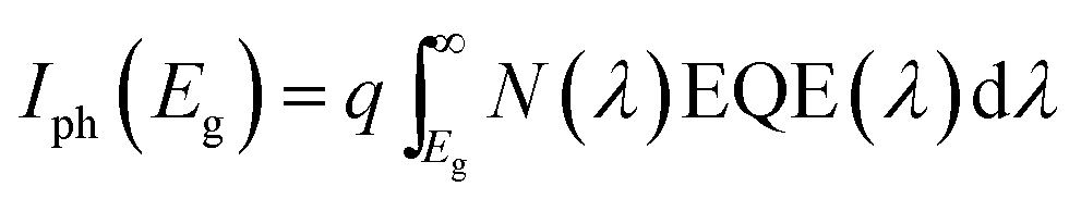
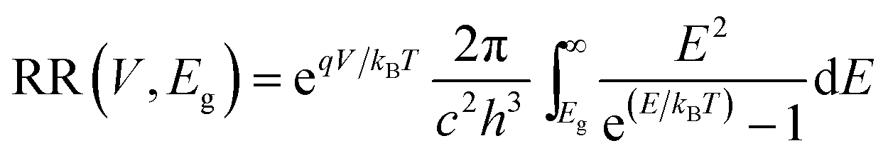
| I(V, Eg) = Iph(Eg) − RR(V, Eg) |
I
ph being the photogenerated current.
with c the speed of light, h the Planck constant and kB the Boltzmann constant. T is the temperature and E is the energy.
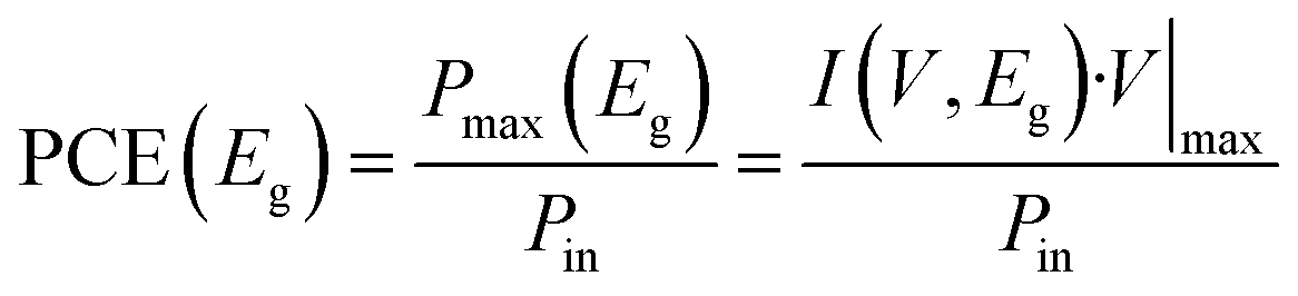
where Pmax is the maximum power extracted from the cell and Pin is the incident sunlight power.
Acknowledgements
The research leading to these results has received funding from the European Research Council under the European Union's Seventh Framework Programme (FP7/2007-2013)/ERC grant agreement no. 307081 (POLIGHT), the Spanish Ministry of Economy and Competitiveness under grant MAT2014-54852-R. MA is grateful to “La Caixa” Foundation for its financial support. AA has received funding from the European Union's Seventh Framework Programme for research, technological development and demonstration under grant agreement no 291771. MS is supported by the co-funded Marie Skłodowska Curie fellowship, H2020 grant agreement no. 665667. FESEM characterization was performed at CITIUS, and we are grateful for its support.Notes and references
- T. Ishihara, J. Lumin., 1994, 60–61, 269 CrossRef CAS.
- M. Hirasawa, T. Ishihara, T. Goto, K. Uchida and N. Miura, Phys. B, 1994, 201, 427 CrossRef CAS.
- K. Tanaka, T. Takahashi, T. Ban, T. Kondo, K. Uchida and N. Miura, Solid State Commun., 2003, 127, 619 CrossRef CAS.
- M. Grätzel, The Light and Shade of Perovskite Solar Cells, Nat. Mater., 2014, 13, 838 CrossRef PubMed.
- N.-G. Park, Mater. Today, 2015, 18, 65 CrossRef CAS.
- W. Zhang, M. Anaya, G. Lozano, M. E. Calvo, M. B. Johnston, H. Míguez and H. J. Snaith, Nano Lett., 2015, 15, 1698 CrossRef CAS PubMed.
- S. D. Stranks and H. J. Snaith, Nat. Nanotechnol., 2015, 10, 391 CrossRef CAS PubMed.
- A. Kojima, K. Teshima, Y. Shirai and T. Miyasaka, J. Am. Chem. Soc., 2009, 131, 6050 CrossRef CAS PubMed.
- S.-H. Kim, C.-R. Lee, J.-H. Im, K.-B. Lee, T. Moehl, A. Marchioro, S.-J. Moon, R. Humphry-Baker, J.-H. Yum, J. E. Moser, M. Grätzel and N.-G. Park, Sci. Rep., 2012, 02, 591 CrossRef PubMed.
- M. M. Lee, J. Teuscher, T. Miyasaka, T. N. Murakami and H. J. Snaith, Science, 2012, 338, 643 CrossRef CAS PubMed.
- J. Burschka, N. Pellet, S.-J. Moon, R. Humphry-Baker, P. Gao, M. K. Nazeeruddin and M. Grätzel, Nature, 2013, 499, 316 CrossRef CAS PubMed.
- W. S. Yang, J. H. Noh, N. J. Jeon, Y. C. Kim, S. Ryu, J. Seo and S. I. Seok, Science, 2015, 348, 1234 CrossRef CAS PubMed.
- S. D. Stranks, G. E. Eperon, G. Grancini, C. Menelaou, M. J. P. Alcocer, T. Leijtens, L. M. Herz, A. Petrozza and H. J. Snaith, Science, 2013, 342, 341 CrossRef CAS PubMed.
- G. Xing, N. Mathews, S. Sun, S. S. Lim, Y. M. Lam, M. Grätzel, S. Mhaisalkar and T. C. Sum, Science, 2013, 342, 344 CrossRef CAS PubMed.
- J. P. Correa Baena, M. Anaya, G. Lozano, W. Tress, K. Domanski, M. Saliba, T. Matsui, T. J. Jacobsson, M. E. Calvo, A. Abate, M. Grätzel, H. Míguez and A. Hagfeldt, Adv. Mater., 2016 DOI:10.1002/adma.201600624.
- See NREL's Efficiency Chart: http://www.nrel.gov/ncpv/images/efficiency_chart.jpg for the latest certified efficiency update.
- F. Deschler, M. Price, S. Pathak, L. E. Klintberg, D.-D. Jaraush, R. Higler, S. Hüttner, T. Leijtens, S. D. Stranks, H. J. Snaith, M. Atatüre, R. T. Phillips and R. H. Friend, J. Phys. Chem. Lett., 2014, 5, 1421 CrossRef CAS PubMed.
- M. Anaya, J. F. Galisteo-López, M. E. Calvo, C. López and H. Míguez, J. Phys. Chem. Lett., 2016, 120, 3071 CrossRef CAS PubMed.
- W. Tress, N. Marinova, T. Moehl, S. M. Zakeeruddin, M. K. Nazeeruddin and M. Grätzel, Energy Environ. Sci., 2015, 8, 995 Search PubMed.
- N. Tripathi, M. Yanagida, Y. Shirai, T. Masuda, L. Han and K. Miyano, J. Mater. Chem. A, 2015, 3, 12081 RSC.
- H.-S. Kim, I.-H. Jang, N. Ahn, M. Choi, A. Guerrero, J. Bisquert and N.-G. Park, J. Phys. Chem. Lett., 2015, 6, 4633 CrossRef CAS PubMed.
- A. Abate, S. Paek, F. Giordano, J.-P. Correa-Baena, M. Saliba, P. Gao, T. Matsui, J. Ko, S. M. Zakeeruddin, K. H. Dahmen, A. Hagfeldt, M. Grätzel and M. K. Nazeeruddin, Energy Environ. Sci., 2015, 8, 2946 Search PubMed.
- M. Saliba, T. Matsui, J.-Y. Seo, K. Domanski, J.-P. Correa-Baena, M. K. Nazeeruddin, S. M. Zakeeruddin, W. Tress, A. Abate, A. Hagfeldt and M. Grätzel, Energy Environ. Sci., 2016, 9, 1989 Search PubMed.
- H. Back, G. Kim, J. Kim, J. Kong, T. K. Kim, H. Kang, H. Kim, J. Lee, S. Lee and K. Lee, Energy Environ. Sci., 2016, 9, 1258 Search PubMed.
- A. Walsh, J. Phys. Chem. C, 2015, 119, 5755 CrossRef CAS PubMed.
- C. C. Stoumpos, L. Frazer, D. J. Clark, Y. S. Kim, S. H. Rhim, A. J. Freeman, J. B. Ketterson, J. I. Jang and M. G. Kanatzidis, J. Am. Chem. Soc., 2015, 137, 6804 CrossRef CAS PubMed.
- C. C. Stoumpos, C. D. Malliakas and M. G. Kanatzidis, Inorg. Chem., 2013, 52, 9019 CrossRef CAS PubMed.
- N. K. Noel, S. D. Stranks, A. Abate, C. Wehrenfennig, S. Guarnera, A.-A. Haghighirad, A. Sadhanala, G. E. Eperon, S. K. Pathak, M. B. Johnston, A. Petrozza, L. M. Herz and H. J. Snaith, Energy Environ. Sci., 2014, 7, 3061 Search PubMed.
- F. Hao, C. C. Stoumpos, D. H. Cao, R. P. H. Chang and M. G. Kanatzidis, Nat. Photonics, 2014, 8, 489 CrossRef CAS.
- F. Zuo, S. T. Williams, P.-W. Liang, C.-C. Chueh, C.-Y. Liao and A. K.-Y. Jen, Adv. Mater., 2014, 26, 6454 CrossRef CAS PubMed.
- F. Hao, C. C. Stoumpos, P. Guo, N. Zhou, T. J. Marks, R. P. H. Chang and M. G. Kanatzidis, J. Am. Chem. Soc., 2015, 137, 11445 CrossRef CAS PubMed.
- Y. Ogomi, A. Morita, S. Tsukamoto, T. Saitho, N. Fujikawa, Q. Shen, T. Toyoda, K. Yoshino, S. S. Pandey, T. Ma and S. Hayase, J. Phys. Chem. Lett., 2014, 5, 1004 CrossRef CAS PubMed.
- H.-J. Feng, T. R. Paudel, E. Y. Tsymbal and X. C. Zeng, J. Am. Chem. Soc., 2015, 137, 8227 CrossRef CAS PubMed.
- F. Hao, C. C. Stoumpos, R. P. H. Chang and M. G. Kanatzidis, J. Am. Chem. Soc., 2014, 136, 8094 CrossRef CAS PubMed.
- T. Yokoyama, D. H. Cao, C. C. Stoumpos, T.-B. Song, Y. Sato, S. Aramaki and M. G. Kanatzidis, J. Phys. Chem. Lett., 2016, 7, 776 CrossRef CAS PubMed.
- Y. Takahashi, R. Obara, Z.-Z. Lin, Y. Takahashi, T. Naito, T. Inabe, S. Ishibashi and K. Terakura, Dalton Trans., 2011, 40, 5563 RSC.
- M. Filipič, P. Löper, B. Niesen, S. De Wolf, J. Krč, C. Ballif and M. Topič, Opt. Express, 2015, 23, A263–A278 CrossRef PubMed.
- S. Albrecht, M. Saliba, J. P. Correa-Baena, F. Lang, L. Kegelmann, M. Mews, L. Steier, A. Abate, J. Rappich, L. Korte, R. Schlatmann, M. K. Nazeeruddin, A. Hagfeldt, M. Grätzel and B. Rech, Energy Environ. Sci., 2016, 9, 81 Search PubMed.
- F. Fu, T. Feurer, T. Jäger, E. Avancini, B. Bissig, S. Yoon, S. Buecheler and A. N. Tiwari, Nat. Commun., 2015, 6, 8932 CrossRef CAS PubMed.
- D. P. McMeekin, G. Sadoughi, W. Rehman, G. E. Eperon, M. Saliba, M. T. Hörantner, A. Haghighirad, N. Sakai, L. Korte, B. Rech, M. B. Johnston, L. M. Herz and H. J. Snaith, Science, 2016, 351, 151 CrossRef CAS PubMed.
- M. Anaya, G. Lozano, M. E. Calvo, W. Zhang, M. B. Johnston, H. J. Snaith and H. Míguez, J. Phys. Chem. Lett., 2015, 6, 48 CrossRef CAS PubMed.
- T. J. Jacobsson, L. J. Schwan, M. Ottosson, A. Hagfeldt and T. Edvinsson, Inorg. Chem., 2015, 54, 10678 CrossRef CAS PubMed.
- W. Nie, H. Tsai, R. Asadpour, J.-C. Blancon, A. J. Neukirch, G. Gupta, J. J. Crochet, M. Chhowalla, S. Tretiak, M. A. Alam, H.-L. Wang and A. D. Mohite, Science, 2015, 347, 522 CrossRef CAS PubMed.
- J. Im, C. C. Stoumpos, H. Jin, A. J. Freeman and M. G. Kanatzidis, J. Phys. Chem. Lett., 2015, 6, 3503 CrossRef CAS PubMed.
- W. Shockley and H. J. Queisser, J. Appl. Phys., 1961, 32, 510 CrossRef CAS.
- J. H. Heo and S. H. Im, Adv. Mater., 2015 DOI:10.1002/adma.201501629.
- J. P. Correa-Baena, L. Steier, W. Tress, M. Saliva, S. Neutzner, T. Matsui, F. Giordano, T. J. Jacobsson, A. R. S. Kandada, S. M. Zakeeruddin, A. Petrozza, A. Abate, M. K. Nazeeruddin, M. Grätzel and A. Hagfeldt, Energy Environ. Sci., 2015, 8, 2928 Search PubMed.
- N. J. Jeon, J. H. Noh, Y. C. Kim, W. S. Yang, S. Ryu and S. I. Seok, Nat. Mater., 2014, 13, 897 CrossRef CAS PubMed.
- P. Löper, M. Stuckelberger, B. Niesen, J. Werner, M. Filipič, S.-J. Moon, J.-H. Yum, M. Topič, S. De Wolf and C. Ballif, J. Phys. Chem. Lett., 2015, 6, 66 CrossRef PubMed.
Footnotes |
| † Electronic supplementary information (ESI) available. See DOI: 10.1039/c6ta04840d |
| ‡ These authors contributed equally. |
| This journal is © The Royal Society of Chemistry 2016 |