
 Open Access Article
 This Open Access Article is licensed under a Creative Commons Attribution-Non Commercial 3.0 Unported Licence
Investigation of morphological degradation of P3HT:PCBM bulk heterojunction films exposed to long-term host solvent vapor†
Weijia
Wang‡
a,
Shuai
Guo‡
a,
Eva M.
Herzig
b,
Kuhu
Sarkar
a,
Markus
Schindler
a,
David
Magerl
a,
Martine
Philipp
a,
Jan
Perlich
c and
Peter
Müller-Buschbaum
*a
aTechnische Universität München, Physik-Department, Lehrstuhl für Funktionelle Materialien, James-Franck-Str. 1, 85748 Garching, Germany. E-mail: muellerb@ph.tum.de; Fax: +49-89-289-12473; Tel: +49-89-289-12451
bTechnische Universität München, Munich School of Engineering, Herzig Group, Lichtenbergstr. 4, 85748 Garching, Germany
cDeutsches Elektronen-Synchrotron DESY, Notkestraße 85, 22603 Hamburg, Germany
First published on 1st February 2016
Abstract
Solution-based processing procedures are widely used during the fabrication of polymer solar cells both on the lab scale and in industrial applications. The understanding of device stability in its host solvent vapor atmosphere is of great significance to the fabrication, encapsulation and storage. Solar cells with poly(3-hexylthiophene):[6,6]-phenyl-C61 butyric acid methyl ester (P3HT:PCBM) bulk heterojunction (BHJ) active layers are prepared with different solvents of chlorobenzene, toluene, xylene and dichlorobenzene. The stability is investigated via exposure to their respective host solvent vapor for a long period. All solar cells strongly degrade after exposure to solvent vapor for long-term and only the dichlorobenzene-related device still shows reasonable function. The morphology of P3HT:PCBM BHJ films is probed using optical microscopy, atomic force microscopy, grazing incidence small and wide angle X-ray scattering and absorption measurements. The solvent induced PCBM crystallization is identified as the main reason for device failure.
Introduction
Organic photovoltaic (OPV) devices as a new generation of solar cells have attracted significant attention, as they present a promising route towards cost-efficient solar power conversion.1–6 The main advantages of OPV devices are related to their potentially low cost, light weight, flexibility and easy processing.7–10 To date, the power conversion efficiency (PCE) of OPV devices has exceeded 9%.11–13 However, the commercial application is still hindered by the poor stability of the devices.14–16As a consequence, the degradation of OPV devices has received a high level of attention.17,18 It was reported that the photovoltaic performance of OPV devices degraded pronouncedly, if they were exposed to oxygen and/or water.19 Thus, suitable encapsulation was developed as an essential procedure to protect solar cells from ambient oxygen and moisture to extend their lifespan for daily applications.20–23 So far, the focus has been mainly on the degradation of the final device and thus on the influence of degradation caused by exposure to oxygen and water. However, besides oxygen and water, the impact of an organic solvent atmosphere also needs to be taken into consideration, since OPV devices are frequently exposed to it, in particular during their fabrication and handling. As is known, most of the OPVs' active layers are prepared by wet chemical processes, such as printing, spray coating, spin coating and blade coating, which to date mostly use organic solvents. The solar cell fabrication typically is done in a closed environment and lasts for several hours up to a few days. During this time the solar cells are exposed to a certain amount of organic solvents. For a fixed production route, the most accessible solvent atmosphere originates from the host solvent during the active layer preparation. For example, a solar cell with the active layer prepared out of chlorobenzene will get likely exposed to chlorobenzene atmosphere during the subsequent handling steps. Since encapsulation is commonly installed as the final device fabrication step, it cannot have any beneficial influence during device fabrication and handling.
As is well known, suitable solvent vapor annealing and non-solvent swelling treatment have been widely investigated to enhance the solar cell efficiency.24,25 However, these are entirely different studies from the case that the sample is unintendedly exposed to its host solvent vapor. The majority of investigations of suitable solvent vapor annealing aim to improve the solar cell efficiency by strictly controlling the annealing conditions such as selecting a suitable solvent vapor, optimizing the time for annealing or mixing different solvents to form the vapor.26–30 It was shown that solvent vapor annealing for a short period such as for several minutes could lead to a more favorable polymer–fullerene BHJ morphology and enhance the crystalline order within the photoactive layer and therefore increase the conductivity and photovoltaic performance.26,31,32 In contrast, the unintended exposure to its host solvent vapor might have entirely different impacts. Chang et al. reported that organic BHJ solar cells reabsorbed the solvent even after the thermal annealing step in a glove box, causing a decreased PCE of the solar cells.33
In theory, solvent vapor annealing is similar to normally used thermal annealing, which enables the molecules of both components to move and accordingly to form a more thermodynamically favorable morphology. The annealing process has a non-monotonic impact in the device performance. The appropriate timescales and temperatures of thermal annealing are required for producing the most efficient organic solar cells. However, overheating can induce the degradation in solar cell efficiency. Treat et al. observed that micron-scale PCBM crystals were formed upon thermal annealing for long periods at 180 °C and it was considered as the main reason for degradation of the efficiency of the final device.34 Therefore, generally much attention is paid to the temperature and time control for the thermal annealing process. However, the long-term effects of the solvent atmosphere generated during active layer preparation are not readily noticeable. To our knowledge, fundamental investigations regarding the influence of long-term exposure to solvent vapor on the morphology of photoactive layers of organic BHJ solar cells are still limited. Furthermore, the host solvent vapor might have different influence on device stability, especially for the fact that the freshly prepared solar cell with the active layer prepared out of different solvents could function normally. In the present work, the influence of long-term host solvent vapor on the morphology of active layers is investigated. We select the model system poly(3-hexylthiophene):[6,6]-phenyl-C61 butyric acid methyl ester (P3HT:PCBM) with a bulk heterojunction (BHJ) morphology, because it is still the most studied system in the OPV area, despite its very moderate efficiency. Chlorobenzene, toluene, xylene or dichlorobenzene as host solvents are commonly used to prepare P3HT:PCBM solutions, which are transferred into the active layers of the solar cells via a wet chemical deposition process. Although for all these solvents the freshly prepared solar cells work well, they might still have different influence on the long-term stability of the device during the fabrication. Therefore, the basic understanding of the impact of their host solvent atmospheres on the stability of the solar cells, in particular on the active layers, could be quite beneficial for enhancing the lifetime of the device.35,36 With the purpose of observing the influence of these organic solvents with respect to the morphology and performance of P3HT:PCBM solar cells, we decided to mimic long time processes with the exposure to a solvent atmosphere. The morphology of the corresponding photoactive layer is probed with real and reciprocal space methods and linked with the device performance after an exposure to solvent vapor. The morphology and crystallinity of the pristine samples were already analyzed in detail in our previous work.35,36 In addition, the solar cell performance of pristine and post-treated devices are compared. Post-treated samples refer to the solar cells or the corresponding photoactive layers which have been kept in one out of four different solvents vapors for 5 days, separately.
The photovoltaic performance of the solar cells is evaluated by current–voltage (J–V) characteristics. Direct imaging techniques such as optical microscopy and atomic force microscopy (AFM) are applied to study the BHJ film surface morphologies. Grazing incidence small angle X-ray scattering (GISAXS) measurements are carried out to probe the inner film morphologies. Additionally, the crystalline structures of the P3HT:PCBM components are investigated using grazing incidence wide angle X-ray scattering (GIWAXS) and UV/vis absorption spectroscopy. As a main result, after long-term exposure to host solvent vapor the solar cell efficiency is mainly affected by the formation of large PCBM crystals in the photoactive layer.
Experimental section
Materials
Poly(3-hexylthiophene) (P3HT) was purchased from Rieke Metals, Inc., with an average molecular weight Mw of 50 kg mol−1 and a regioregularity of more than 95%. [6,6]-Phenyl-C61 butyric acid methyl ester (PCBM) was obtained from Nano-C with a purity of 99.5%. Poly(3,4-ethylenedioxythiophene):poly(styrenesulfonate) (PEDOT:PSS) (PH1000) solution was purchased from Ossila, with a PEDOT to PSS weight ratio of 1![[thin space (1/6-em)]](https://www.rsc.org/images/entities/char_2009.gif) :2.5. Chlorobenzene, toluene, xylene and dichlorobenzene were obtained from Carl Roth and were used as supplied.
:2.5. Chlorobenzene, toluene, xylene and dichlorobenzene were obtained from Carl Roth and were used as supplied.
Sample preparation
P3HT was dissolved in the host solvent until complete dissolution, and then the P3HT solution was added to the PCBM powder in a weight ratio of 1:1. The final solution was stirred overnight at room temperature. Chlorobenzene, toluene, xylene and dichlorobenzene were used as four different host solvents. In order to obtain similar film thickness values, the final concentrations were adapted to 20 mg ml−1 (chlorobenzene), 18 mg ml−1 (toluene), 24 mg ml−1 (xylene) and 30 mg ml−1 (dichlorobenzene).
For the solar cell device fabrication, indium tin oxide (ITO) was partially removed from the glass substrates by chemical etching and then cleaned in a sequence using Alconox solution, ethanol, acetone and 2-propanol in an ultrasonic bath. The cleaned ITO-covered glass substrates were treated with oxygen plasma for 10 minutes. The PEDOT:PSS solution was filtered by PVDF filters with a pore size of 0.45 μm and then deposited via spin-coating (3000 rpm, 60 s) on the ITO-covered glass substrates. Next, the samples were annealed for 10 minutes at 150 °C. Afterwards, P3HT:PCBM films were deposited via spin-coating (2000 rpm, 30 s) on top of the prepared PEDOT:PSS layers. For the degradation, four glass chambers with a volume of 0.7 L were used. 10 ml of the host solvent was injected at the bottom of each chamber to generate a saturated vapor atmosphere at 25 °C. The corresponding samples were positioned 54 mm above the base when the chamber is close to saturation of the solvent atmosphere. The vapor pressures of chlorobenzene, toluene, xylene, and dichlorobenzene are 12.0 mmHg, 28.4 mmHg, 6.6 mmHg, and 1.4 mmHg at 25 °C, which refer to the atmospheric solvent concentrations of 6.45 × 10⁻⁴ mol l−1, 1.53 × 10⁻³ mol l−1, 3.55 × 10⁻⁴ mol l−1, and 7.3 × 10⁻⁵ mol l−1, respectively. The storage time was 5 days. To finalize the device, aluminum electrodes were deposited by physical vapor deposition.
For UV/vis absorption, optical microscopy, AFM, GISAXS and GIWAXS measurements, the P3HT:PCBM solutions were spin-coated on acid cleaned glass substrates instead of ITO-coved glass substrates.
Measurements
J–V characteristics of the solar cells were probed under AM1.5 illumination (1000 W m−2) and recorded by using a source meter, Keithley 2400. To calibrate the solar simulator Solar Constant 1200 (K.H. Steuernagel Lichttechnik GmbH), a silicon-based reference solar cell was used. In total, about 12 solar cells were probed for each solvent. Each pixel area was defined with a shadow mask and measured by using a calibrated microscope.The UV/vis absorption spectra were derived from the transmission measurements, which were performed with a UV/vis spectrometer Lambda 35 (PerkinElmer), with a wavelength range from 190 to 1100 nm. The measurements were carried out with a scan speed of 120 nm min−1 and a slit width of 1 nm under ambient conditions.
AFM Autoprobe CP Research (Veeco Metrology Group) was used to probe the surface morphologies of BHJ films in tapping mode. Conical shaped cantilevers with gold coating were used. The resonance frequency of the cantilever was set around 60 kHz. AFM measurements were performed under ambient conditions.
GISAXS measurements were carried out at the synchrotron beamline BW4 of the DORIS III storage ring at DESY, Hamburg, Germany.37,38 The wavelength of the X-rays was 0.138 nm. A constant incident angle (αi = 0.4°) was chosen to make sure that the beam penetrated the whole film. Thus, surface and inner film structures were probed. The sample-detector distance was 2.088 m to access a reasonable qy range. A MarCCD area detector was used. In order to analyze the two dimensional (2D) GISAXS data, horizontal line cuts were performed. A model in the framework of the distorted wave Born approximation (DWBA) was applied to describe the horizontal line cuts.39 As the incident angle is fixed, the influence of the transmission functions can be ruled out and the scattering factor is probed. The scattering factor is composed of form factor and structure-factor contributions. The form factor captures the shape and size of individual objects, such as cylinder or sphere. In polymer systems, cylinder form factors are quite common, especially for P3HT:PCBM BHJ films.14,40 The polydispersity of the objects is included via a Gaussian distribution function. A one-dimensional paracrystalline lattice is assumed for the arrangement of scattering objects, as introduced by Hosemann et al.41 The model we employed is local monodisperse approximation (LMA), meaning that the total scattered intensity can be approximated by incoherently superposing the scattered intensity of individual objects without interaction with the object with distinct structures.14 In this work, three cylinder-shaped objects have to be assumed to properly describe the GISAXS data (for sketch, see Fig. S1 in the ESI†). Fitting with a single set of form and structure factors or with two sets of form and structure factors showed significant deviations between best fits and data.
GIWAXS measurements were performed at the same beamline with an incident angle of 0.2° and a sample-detector distance of 0.11 m. Data were collected with the same MarCCD area detector. To make the geometric correction and two-dimensional intensity reshaping, a grazing-incidence X-ray scattering graphical user interface (GIXSGUI) was used. GIXSGUI is an open source program, which was developed by Advanced Photon Source, Argonne National Laboratory, USA.
Results and discussion
Solar cell performance
The organic BHJ solar cells have been built following a layered architecture of glass/ITO/PEDOT:PSS/P3HT:PCBM/aluminum. In order to probe the differences of the photovoltaic performance between pristine solar cells and post-treated solar cells and thereby examine the degradation of the devices, both series of solar cells are characterized with the J–V curves. The obtained results are shown in Fig. 1. The relevant photovoltaic characteristics, such as PCE, short circuit current (JSC), open circuit voltage (UOC) and fill factor (FF), are extracted from the J–V curves and listed in Table 1. The PCE values of the pristine solar cells are only moderate as compared to what have been reported in the literature in terms of P3HT:PCBM solar cells.42,43 However, the focus of the present investigation was on the degradation, which is a relative loss in device performance.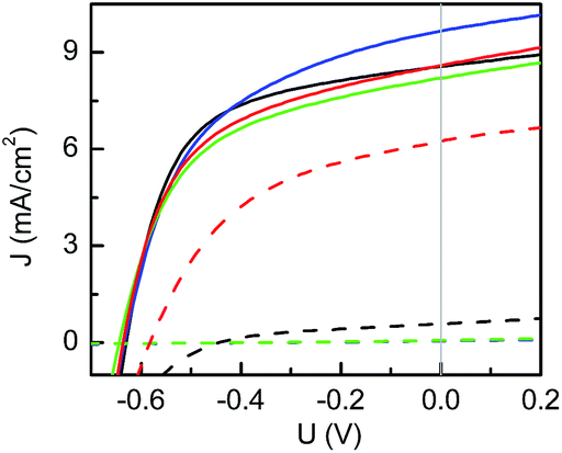 | ||
| Fig. 1 J–V curves of pristine P3HT:PCBM solar cells (solid lines) and post-treated P3HT:PCBM solar cells (dashed lines) processed using chlorobenzene (black), toluene (blue), xylene (green) and dichlorobenzene (red), respectively. | ||
| Solvent | Device | J SC [mA cm−2] | U OC [V] | FF [%] | η [%] |
|---|---|---|---|---|---|
| Chlorobenzene | Pristine | 8.41 ± 0.12 | −0.63 ± 0.01 | 58 ± 1 | 3.09 ± 0.06 |
| Post-treated | 0.56 ± 0.03 | −0.41 ± 0.01 | 41 ± 1 | 0.09 ± 0.01 | |
| Toluene | Pristine | 9.71 ± 0.06 | −0.61 ± 0.01 | 50 ± 2 | 2.99 ± 0.16 |
| Post-treated | 0.05 ± 0.01 | −0.36 ± 0.03 | 23 ± 1 | 0.01 ± 0.01 | |
| Xylene | Pristine | 8.16 ± 0.37 | −0.63 ± 0.01 | 52 ± 1 | 2.71 ± 0.19 |
| Post-treated | 0.08 ± 0.01 | −0.40 ± 0.01 | 20 ± 1 | 0.01 ± 0.01 | |
| Dichlorobenzene | Pristine | 8.47 ± 0.18 | −0.64 ± 0.01 | 53 ± 1 | 2.85 ± 0.12 |
| Post-treated | 6.15 ± 0.22 | −0.58 ± 0.01 | 47 ± 1 | 1.66 ± 0.07 |
In general, all solar cells demonstrate degradation after long-term exposure to the host solvent vapor (the PCE values significantly degrade). Amongst them, dichlorobenzene-based solar cells show the best remaining J–V performance for post-treated solar cells. After the harsh solvent vapor treatment, the PCE values of 1.66 ± 0.07% remain, which are still more than 50% of the original PCE (2.85 ± 0.12%). In the case of chlorobenzene the solar cell behavior was maintained after exposure to chlorobenzene vapor for 5 days, whereas solar cells exposed to toluene and xylene lose function and fail completely. As seen from Table 1, the degradation is mainly driven by the decrease in JSC. In addition, UOC and FF decrease as well.
To specifically understand the degradation of the investigated solar cells, the morphology of the post-treated P3HT:PCBM films is characterized in detail. The morphology of the pristine active layers was reported in detail in previous studies.35,36
Surface topography
As shown in the optical microscopy images (Fig. 2), all post-treated P3HT:PCBM films exhibit specific surface morphologies. In particular, the samples post-treated with chlorobenzene, toluene and xylene vapors (Fig. 2a–c) exhibit PCBM aggregates in the micron scale. Fig. 2a displays some big flower-shaped PCBM clusters. Paternò et al. observed similar flower-shaped PCBM clusters, which were determined as large PCBM crystalline aggregates based on micro-focused X-ray diffraction experiments.44 For the samples post-treated with toluene and xylene vapors (Fig. 2b and c), more PCBM aggregates with smaller sizes are formed. In Fig. 2c, the lighter yellow regions around the PCBM aggregates are the PCBM depletion regions, which were observed in earlier investigations as well.35 The size distributions of PCBM aggregates in these three different samples are estimated by using the optical microscopy images within the detected surface area (1.02 × 0.82 mm2), as shown in Fig. S2.† With respect to the chlorobenzene-related sample, most of the aggregates reside in the area ranged larger than 1000 μm2, while the toluene and xylene related samples show a similar trend of size distribution mainly in the range from 200 to 600 μm2. Furthermore, the numbers and area fractions of PCBM aggregates are extracted, listed in ESI as Table S1.† The sample post-treated with toluene has the highest number of aggregates of 101, while the chlorobenzene and xylene related samples have 12 and 65 aggregates, respectively. Additionally, the chlorobenzene has the largest PCBM aggregate area fraction of 4.9% as compared to the one related to toluene (3.8%) and xylene (1.8%). However, no micron-sized PCBM aggregates are observed in the dichlorobenzene vapor post-treated sample (Fig. 2d). Thus, the formation of micron-sized PCBM aggregates can be a reason for the observed device degradation.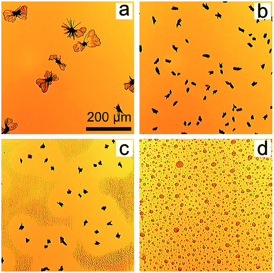 | ||
| Fig. 2 Optical microscopy images of P3HT:PCBM films post-treated with chlorobenzene (a), toluene (b), xylene (c) and dichlorobenzene (d) vapors. All images have an identical size. | ||
To explain the influence of the long-term solvent vapor treatment on the large scale surface morphologies, the impact of the vapor pressure is firstly considered. As dichlorobenzene has the lowest vapor pressure at 25 °C (1.4 mmHg) in comparison with the other used solvents (chlorobenzene, toluene and xylene have values of 12.0 mmHg, 28.4 mmHg and 6.6 mmHg), the total absorption of dichlorobenzene molecules could be limited, when placed in a dichlorobenzene atmosphere. Accordingly, PCBM aggregation is prevented in the dichlorobenzene atmosphere. It was also observed by Hu et al. that the smallest weight percentage increase of P3HT:PCBM films was obtained by dichlorobenzene vapor annealing.45 However, they also observed the maximum weight percentage increase of the P3HT:PCBM sample in chlorobenzene vapor, which is not directly correlated with the vapor pressure anymore. Therefore, the solubility of P3HT and PCBM in distinct solvents is taken into account. For P3HT, the solubility is 33.8 mg ml−1 for chlorobenzene, 1.4 mg ml−1 for toluene, 3.4 mg ml−1 for xylene, and 37.1 mg ml−1 for dichlorobenzene, while for PCBM, the corresponding solubilities are 39.4 mg ml−1, 16.3 mg ml−1, 24.5 mg ml−1 and 35.9 mg ml−1, respectively.45 The largest but the least PCBM aggregates are formed in chlorobenzene-related films, which might be explained by the high vapor pressure, the biggest solubility of PCBM, and the biggest miscibility between P3HT and PCBM. On the other hand, many more PCBM aggregates are observed in toluene and xylene related samples, probably due to the relatively small miscibility between P3HT and PCBM. Similarly, it has been reported that PCBM aggregates were formed in another high PCBM solubility solvent vapor, 2-chlorophenol.46 In more general, both the vapor pressure and the solubility of PCBM in the solvent strongly influence the PCBM aggregate formation.
To gain further insights into the surface morphology on the nanoscale, atomic force microscopy (AFM) measurements are performed on the homogeneous parts of the films rather than on those parts dominated by the formed PCBM aggregates. As it is illustrated in Fig. 3, the type of solvent vapor has significant influence on the nanoscale morphology of the films as well. The samples post-treated with chlorobenzene (Fig. 3a) or toluene vapor (Fig. 3b) show a stripe-like nanomorphology, while the one with xylene vapor treatment (Fig. 3c) shows doughnut-like structures. Large spherical structures are observed on the sample post-treated with dichlorobenzene vapor as shown in Fig. 3d. In general, all post-treated samples exhibit coarsened surface nanostructures as compared to the pristine films, which were probed in our previous work.35 Additionally, all solvent vapor-degraded samples show significantly increased surface roughness values as compared to the initial films. The highest surface root-mean-square (rms) roughness of around 79.8 Å is found for the sample treated with dichlorobenzene. The changes in surface structures might give rise to the observed device degradation, however, it might be also linked to strong changes of the inner film morphologies.
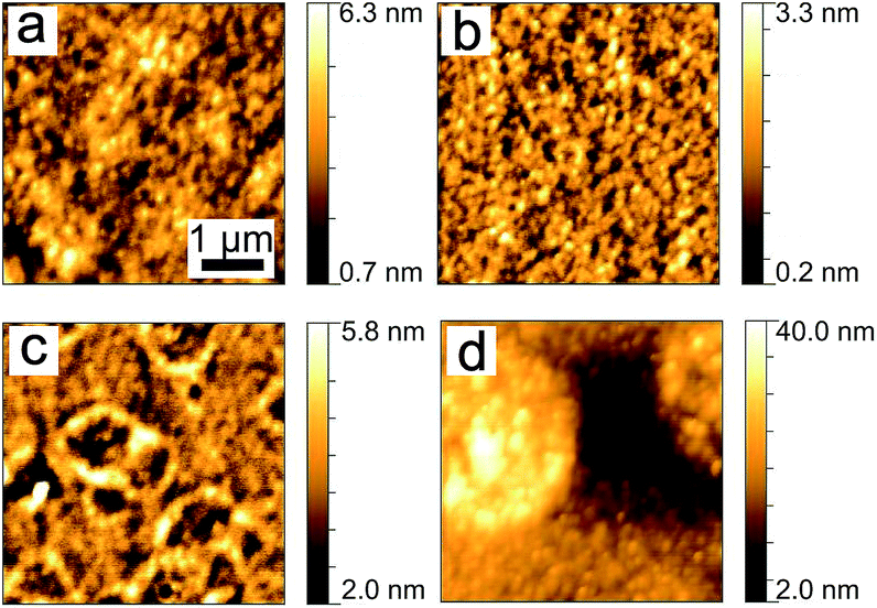 | ||
| Fig. 3 AFM images (4 × 4) μm2 of P3HT:PCBM films, post-treated with chlorobenzene (a), toluene (b), xylene (c) and dichlorobenzene (d) vapors. The corresponding rms roughness values are 8.6 Å, 4.7 Å, 7.8 Å and 79.8 Å, respectively. | ||
Inner film morphology
The inner film morphologies might be different from the surface morphologies that have been revealed using AFM topography measurements.35 As is well known, the inner film morphology of the photoactive layer is significant for the solar cell performance.47–51 To probe the inner morphology of the active layers, GISAXS is a well suited technique which gives statistical information on a mesoscopic length scale.52–55 The 2D GISAXS data of P3HT:PCBM films post-treated with chlorobenzene, toluene, xylene and dichlorobenzene vapors are shown in Fig. 4. A beam stop is used to block the specularly reflected beam (specular peak) to avoid oversaturation of the detector. Yoneda peaks, located at the position of the critical angle (αc), are well visible in all GISAXS measurements.56 Intensity oscillations along the qz direction are found in the 2D GISAXS data of the samples post-treated with chlorobenzene, toluene and xylene vapors. These oscillations are a signature of partially correlated surface roughness arising from the P3HT:PCBM layer following the structure of the substrate underneath.36,57 Correlated roughness is not observed for the dichlorobenzene vapor post-treated sample, because of the relatively high surface roughness as mentioned above. Additionally, for the dichlorobenzene vapor post-treated sample (Fig. 4d), the scattering signal extends further out into the higher qy region as compared to that of the other samples, which is related to the presence of smaller lateral structures. Moreover, prominent Bragg peaks appear in the case of chlorobenzene and toluene exposure (Fig. 4a and b, marked with red arrows). These Bragg peaks are located at qz positions equal to 1.371 nm−1 and 1.379 nm−1, respectively. They are attributed to the Bragg reflection of large PCBM crystallites, which will be carefully discussed in the following GIWAXS measurements. To our knowledge, notable Bragg peaks from PCBM crystallites are rarely reported in 2D GISAXS data.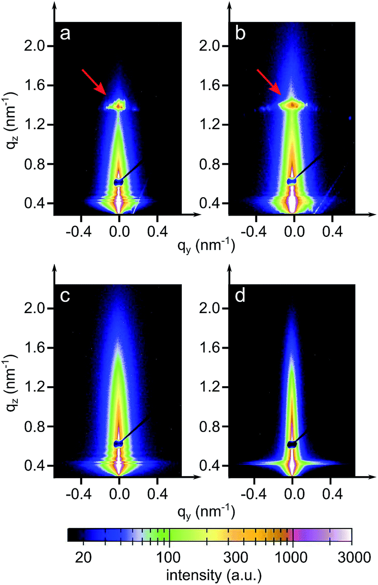 | ||
| Fig. 4 2D GISAXS data of P3HT:PCBM films post-treated with chlorobenzene (a), toluene (b), xylene (c) and dichlorobenzene (d) vapors, respectively. The Bragg peaks are marked with red arrows. The specular peak is shielded with a point-shaped beamstop. | ||
To obtain the lateral structure information of the inner film morphology, horizontal line cuts from the 2D GISAXS data are performed at the P3HT Yoneda peak position (Fig. 5). These line cuts reveal the structure information parallel to the substrate surface. In order to extract the corresponding structural information, the horizontal line cuts are fitted with the model including three form factors and their corresponding structure factors, as described in the experimental section. It means that three prominent substructures exist in the samples. The presence of multiple substructures was reported for P3HT:PCBM BHJ films before.40,58–62 In general, a model assuming the presence of intermixed phases between amorphous P3HT and PCBM, pure P3HT lamellas, and pure PCBM aggregates is well accepted.58,59 However, the details of the observed structures will depend on the used sample-preparation method and on the probed q range. For example, Yin et al. investigated thick drop-cast P3HT:PCBM films by small angle neutron scattering (SANS) focusing on the high q region.60 They observed one substructure when the amount of PCBM was below a certain threshold, while additional large substructures appeared when the amount of PCBM approached 50 vol%.60 Huang and coworkers found two substructures identified as PCBM:P3HT amorphous domains and large PCBM aggregates by GISAXS measurements.61 Verploegen and coworkers used GISAXS to study P3HT:PCBM films and reported two pronounced domains after thermal or solvent annealing.31 With an increased q region towards smaller q values, additional larger structures become accessible. Moseguí González et al. observed three different substructures in spin-coated P3HT:PCBM films using GISAXS.40 A previous study on inverted P3HT:PCBM solar cells also revealed three substructures in P3HT:PCBM films by the in situ GISAXS measurements.62 From the parameters obtained in the fitting results, the nanomorphology of the active layer is estimated. In this model, the structure sizes correspond to the form factors (the radii of the domains with a cylinder shape) and the distances are related to structure factors (center-to-center distances). The corresponding fits are shown in Fig. 5 with solid lines.
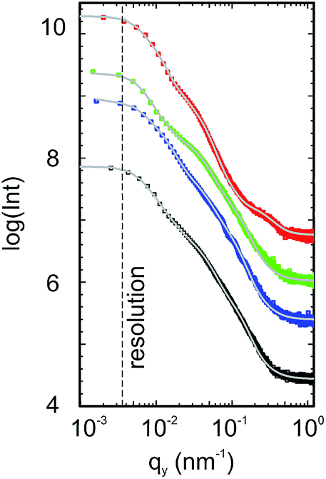 | ||
| Fig. 5 Horizontal line cuts of the 2D GISAXS data of P3HT:PCBM films post-treated using chlorobenzene (black), toluene (blue), xylene (green) and dichlorobenzene (red) vapors. Solid lines (grey) are the fits as explained in the text. The curves are shifted along the intensity axis for clarity. The dashed line represents the resolution limit to larger structures. | ||
The obtained structure sizes and distances are extracted from the fitting results and summarized in Fig. 6. In general, all active layers exhibit three characteristic structures with different sizes. These average structure sizes are on the order of 10 nm, 30 nm and 105 nm with the corresponding distances of around 40 nm, 140 nm and 400 nm. Because all horizontal line cuts were taken at the material specific Yoneda peak of P3HT, where the strongest scattering contribution of P3HT occurs, information about lateral structures formed by P3HT or its voids (PCBM) is gained. We ascribe the structures from the GISAXS data modelling to amorphous P3HT with embedded PCBM, lamellar P3HT, and large PCBM domains. Ruderer et al. observed an average length of PCBM embedded in the amorphous P3HT phase from 3 to 10 nm in grazing incidence small angle neutron scattering measurements, which matches the smallest structures observed in the present work.63 Schaffer et al. considered the intermediate substructure (with form factors from 30 to 40 nm) as P3HT fibers.14 They observed the coarsening of this substructure with illumination and successfully found the correlation between the morphological decay and device degradation. Moreover, P3HT fibers were also reported from scattering experiments on P3HT:PCBM solutions.64,65 The large domains are understood as surface structures as they can be evidenced in line cuts extracted from AFM data as shown in Fig. S3.† Treat et al. also reported a similar morphology for the P3HT:PCBM system66 and Swinnen and coworkers using selected area electron diffraction analysis and transmission electron microscopy showed large phase separation structures between PCBM aggregates and almost pure P3HT as well.67 Since an effective exciton diffusion length of 10 nm was determined for the photoactive material P3HT,47,68 the smallest structures (on the order of 10 nm, plotted in black in Fig. 6) are expected to dominate the main photovoltaic performance of the solar cells. These smallest structures are 11 nm, 12.5 nm, 9.5 nm and 4.5 nm (radii of the domains) for films post-treated with chlorobenzene, toluene, xylene and dichlorobenzene vapors, respectively. Among all of them, the sample post-treated with dichlorobenzene vapor shows a significantly smaller structure size compared to the other three samples, which could be correlated with a relatively higher current density of the final devices. However, regarding the other three samples, the evolved structure sizes are still in the range for efficient exciton dissociation. Therefore, the size of the nanostructures in the active layers cannot be the main reason for the failure of the solar cells post-treated with chlorobenzene, toluene and xylene.
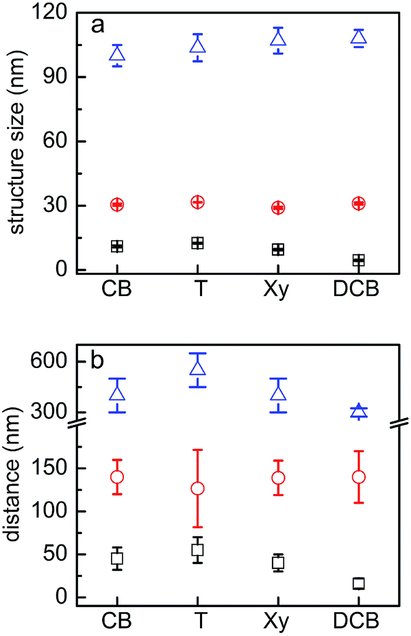 | ||
| Fig. 6 Characteristic structure sizes (a) and distances (b) of P3HT:PCBM films post-treated with chlorobenzene, toluene, xylene and dichlorobenzene vapors. The values are obtained from the fitting parameters of the horizontal line cuts of 2D GISAXS data. | ||
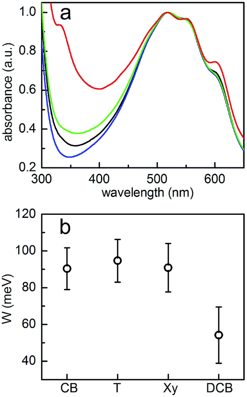
Absorption behavior
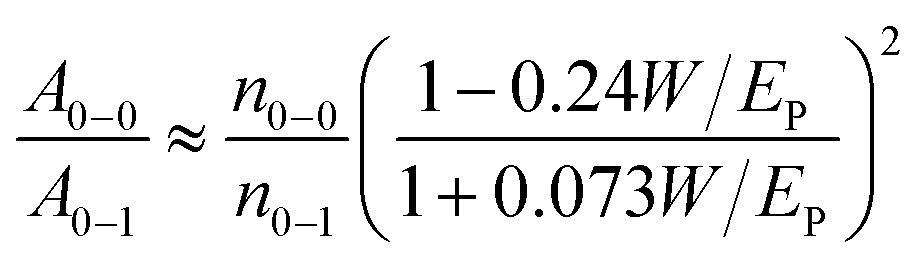
The normalized absorbance spectra of post-treated samples are shown in Fig. 7a. The positions of the main P3HT absorbance peak at around 517 nm and two shoulder-like features around 550 nm and 600 nm do not change with the use of different solvents in the vapor treatment. Both shoulder-like features are attributed to the presence of P3HT crystallites, suggesting that P3HT crystallites are preserved after solvent-vapor treatment. To estimate further information about the P3HT crystalline order, the weakly coupled H-aggregate model is applied:69A0–1 and A0–0 indicate absorbance intensities of the two shoulders at 550 nm and 600 nm. W is the free exciton band width within the P3HT crystalline phase, which can be extracted through the ratio of A0–0 to A0–1. In general, a lower value of W means a higher crystalline order of the P3HT. In the case of P3HT:PCBM based solar cells made from different solvents, typical values of W, as found in the literature, are W = 92 ± 10 meV, W = 76 ± 10 meV and W = 140 ± 10 meV for well working devices.70 As shown in Fig. 7b, the values of W are between 55 ± 15 meV and 95 ± 12 meV in the present study, which means that the crystalline order of the P3HT chains in all samples fully meets the requirements for working devices. In comparison, the dichlorobenzene vapor post-treated sample exhibits the smallest value of W, indicating the highest P3HT crystalline order among all the post-treated samples. Generally, in P3HT:PCBM BHJ solar cells, the P3HT crystalline region affords a high hole mobility, therefore a higher P3HT crystalline order assists to achieve high JSC values. Hence, the higher P3HT crystalline order of the dichlorobenzene-related device contributes to its higher JSC as compared to that of other samples. However, for the other three samples still a sufficient crystalline order of the P3HT chains is found to allow for working solar cells. Therefore, we conclude that the evolution of the crystalline order of P3HT is not a reason for the failure of solar cells, either.
 | ||
| Fig. 7 (a) Normalized absorbance of P3HT:PCBM films treated with chlorobenzene (black), toluene (blue), xylene (green) and dichlorobenzene (red) vapors. (b) The free exciton bandwidth extracted from absorption spectra using the weakly coupled H-aggregate model. | ||
Regarding the PCBM absorbance at around 335 nm, different absorption features are observed for the post-treated samples. Except for the dichlorobenzene vapor post-treated sample, all other three samples show significantly weaker PCBM absorbance. As illustrated from the optical microscopy images (Fig. 2), large PCBM aggregates are formed in these three samples, which can strongly scatter the light and accordingly lower the PCBM absorbance. Liu et al. reported similar absorbance features, when large PCBM aggregates were formed in P3HT:PCBM films.71 Overall, the PCBM aggregates might hinder P3HT crystallization during the solvent vapor treatment, which explains why the sample with dichlorobenzene vapor post-treatment has the highest P3HT crystalline order. However, the formation of large PCBM crystals appears to have a larger effect on the solar cells degradation.
Crystalline structure
In order to further investigate the crystalline structure, GIWAXS measurements are performed. The 2D GIWAXS data are displayed in Fig. 8. Significant differences in the scattering patterns among all the samples are observed, which are dominated by PCBM scattering signals. The pronounced Bragg diffraction spots denoted by three round circles in Fig. 8a (chlorobenzene treatment) and 8b (toluene treatment) indicate the formation of large and well-ordered PCBM crystallites. Verploegen et al. had also observed distinct peaks in 2D GIWAXS data upon heating PCBM films to 205 °C, but with a different appearance.31 For a quantitative analysis, their respective positions in terms of qxy, qz and q values are listed in Table 2. For each specific Bragg diffraction spot, both samples show similar q values. Thus, it is inferred that the same PCBM crystalline phase is formed in chlorobenzene and toluene vapor post-treated samples. This finding is in agreement with an earlier study, as Colle et al. reported that samples prepared from chlorobenzene and toluene showed the same PCBM crystalline phase.72 Additionally, it is noticed that the qxy and qz values of peak 1 (donated as black circles in Fig. 8a and b) show flipped coordinates in these two samples, suggesting that opposite PCBM orientations are formed in both samples. For xylene and dichlorobenzene less pronounced scattering features are observed. The 2D GIWAXS data of the xylene vapor post-treated sample (Fig. 8c) present patchy broad intensity rings, indicating the presence of randomly distributed, relatively small PCBM crystallites. In contrast, the 2D GIWAXS data of the sample post-treated with dichlorobenzene vapor (Fig. 8d) are dominated by a broad ring-like scattering feature originating from amorphous PCBM. No more well-oriented crystallites are detected, which was as well frequently observed in P3HT:PCBM films after thermal annealing.63 Moreover, it is found that the PCBM crystal sizes depend on the solvents. Larger PCBM crystallites are formed in the sample post-treated with higher vapor pressures and higher PCBM solubility solvents (toluene and chlorobenzene). However, no PCBM crystallites are found in the sample post-treated with the solvent having a low vapor pressure and large miscibility between P3HT and PCBM, even for the fact that it has high PCBM solubility (dichlorobenzene). Furthermore, the tube cuts at the position of PCBM crystallites (q from 12 to 15.5 nm−1) are made. The resulting figure is shown in the ESI as Fig. S4.† For the samples post-treated with chlorobenzene and toluene, main peaks locate around ±15, ±30, ±45, ±60, and ±75°. While the sample post-treated with xylene show more and broadly distributed peaks, indicating no preferential orientation. For the dichlorobenzene related sample, no peak is observed, suggesting the amorphous PCBM. In addition, the sample post-treated with chlorobenzene has the highest and sharpest peak, resulting from the large PCBM crystallites, which is consistent with the observation from optical microscopy images. Therefore, by selecting a suitable solvent vapor, the formation of the PCBM crystalline structure is strongly affected. Correlating the information of PCBM crystalline structures with the final solar cell performance, it is inferred that the formation of PCBM crystallites could be the most serious reason for the solar cell failure. Treat et al. also obtained a similar conclusion that the micron-scale PCBM crystallites formed after long time thermal annealing were correlated with the degradation in photo conversion efficiency.34 During the solvent post-treatment, the PCBM molecules tend to crystallize; meanwhile a large number of PCBM aggregates are formed. It leads to an extremely large domain size of the PCBM phase, in a micron-scale, as shown in optical microscopy images (Fig. 2).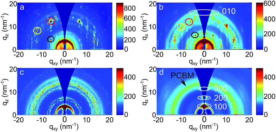 | ||
| Fig. 8 2D GIWAXS data of P3HT:PCBM films post-treated with chlorobenzene (a), toluene (b), xylene (c) and dichlorobenzene (d) vapors. Dominant PCBM Bragg peak 1, peak 2 and peak 3 are marked as black, yellow and red circles in (a) and (b), respectively. | ||
| Solvent | Peak 1 [nm−1] | Peak 2 [nm−1] | Peak 3 [nm−1] | ||||||
|---|---|---|---|---|---|---|---|---|---|
| q xy | q z | q | q xy | q z | q | q xy | q z | q | |
| Chlorobenzene | 5.98 | 3.95 | 7.17 | 11.92 | 7.95 | 14.33 | 5.67 | 11.77 | 13.06 |
| Toluene | 3.90 | 5.95 | 7.17 | 9.80 | 9.03 | 13.33 | 5.70 | 11.73 | 13.04 |
Additionally, detailed information about the P3HT crystals is obtained as well. As shown in the 2D GIWAXS data (Fig. 8), all films have (100) and (010) Bragg peaks of the polymer, indicating the presence of P3HT crystallites. This observation is consistent with the conclusions from the above absorbance measurements. Moreover, for the sample with dichlorobenzene vapor post-treatment, the intensity of the (010) Bragg peak along the horizontal direction exceeds that in vertical direction, suggesting that edge-on oriented P3HT crystallites are dominating. Instead, for the other three samples a face-on dominated orientation is observed. For a quantitative analysis, the vertical and horizontal sector integrals are taken from the 2D GIWAXS data and are shown in Fig. 9a and b. Due to the high intensities of (100) Bragg peaks of P3HT and the strong PCBM Bragg peaks at q < 5 nm−1, the vertical sector integral with the q range above 5 nm−1 is shown in Fig. 9c separately. For all samples (100) Bragg peaks are found with their higher orders. The (200) and (300) peaks are visible in the vertical direction (Fig. 9c). In the horizontal direction the (100) peaks are also found but no higher orders are seen (Fig. 9a). Additionally, (010) Bragg peaks are found in both directions for all samples. To obtain further information in terms of lattice constants, the detected Bragg peaks are fitted with Gaussian functions to determine the peak positions. As listed in Table 3, all samples show similar lattice constants around 1.70 nm in horizontal (100) direction and 0.4 nm (010) in both directions, which are consistent with P3HT lattice constants reported in other studies.35 However, the values in the vertical (100) direction are slightly distinct, which is probably due to the fact that the interference with the strong scattering signals of PCBM crystals and the GISAXS data. It is concluded that the lattice constants of P3HT are independent of the selected solvent vapor. In agreement with the conclusions from the absorption measurements, for all post-treated samples, the crystalline order of the P3HT chains cannot be the reason for the degradation of the solvent-treated solar cells.
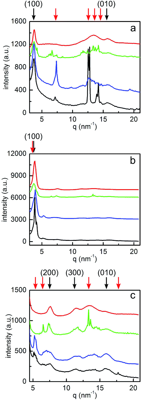 | ||
| Fig. 9 Horizontal (a) and vertical (b) sector integrals performed on 2D GIWAXS data of P3HT:PCBM films post-treated with chlorobenzene (black), toluene (blue), xylene (green) and dichlorobenzene (red) vapors. Vertical sector integrals above 5 nm−1 are shown in (c). The black and red arrows denote the scattering signal from P3HT and PCBM crystallites, respectively. The curves are shifted along the intensity axis for clarity. | ||
| Solvent | Lattice constant [nm] | |||
|---|---|---|---|---|
| (100) ha | (010) h | (100) vb | (010) v | |
| a h represents the horizontal sector integral. b v represents the vertical sector integral. | ||||
| Chlorobenzene | 1.70 ± 0.001 | 0.40 ± 0.002 | 1.71 ± 0.005 | 0.40 ± 0.004 |
| Toluene | 1.70 ± 0.005 | 0.40 ± 0.003 | 1.66 ± 0.018 | 0.40 ± 0.004 |
| Xylene | 1.71 ± 0.065 | 0.40 ± 0.002 | 1.71 ± 0.005 | 0.40 ± 0.004 |
| Dichlorobenzene | 1.70 ± 0.009 | 0.40 ± 0.001 | 1.64 ± 0.001 | 0.40 ± 0.039 |
Moreover, we selected the xylene-related sample as an example to investigate the impact of solvent exposure time and compare with the common thermal annealing treatment. The changes in the morphology from 1 to 5 days are observed with GISAXS and GIWAXS. The resulting data are included in the ESI as Fig. S5.† In general we find similar trends as reported for the thermal annealing process,34 including coarsening of the structures and formation of PCBM crystals with increasing annealing time.
Fig. 10 summarizes in a schematic way how solvent post-treatment influences the morphology and crystalline order of the P3HT:PCBM samples at the microscale. The grey dots are related to PCBM, while the red tangled lines represent the amorphous P3HT and the parallel lines the crystalline P3HT phase. The sample post-treated with dichlorobenzene (Fig. 10d) shows relatively higher P3HT crystallinity and an edge-on dominated crystal orientation as compared to the other three samples. However, in general all samples have reasonable crystalline P3HT domains to allow for well working solar cells. Therefore, the P3HT crystalline structure is not strongly degraded by the long-term solvent vapor treatment and accordingly it is not the key factor for the solar cell degradation and failure. On a larger scale, the phase separation of P3HT and PCBM causes a domain structure in the range for an efficient exciton dissociation, although in detail the different samples show slightly different lateral structure sizes. On a larger scale on the order of exciton diffusion length, the lateral domain structures induced by the phase separation of P3HT and PCBM differ only in the details among the different samples. Thus, the nanomorphology of all the samples should be still satisfactory to achieve well working solar cells. However, on the micrometer scale important differences in the morphology are found. It is clearly noticed that only the sample post-treated with dichlorobenzene vapor does not form large PCBM crystallites, while in all the other three samples the PCBM crystallizes in very large domains. Consequently, it is concluded that PCBM is more sensitive to the selected solvent vapor as compared to P3HT. We ascribe the formation of PCBM crystallites as the main reason for the observed solar cell failure.
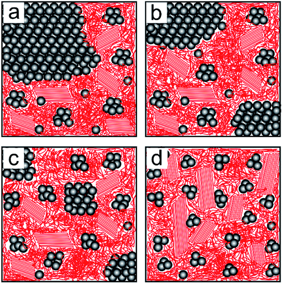 | ||
| Fig. 10 Schematic morphology of P3HT:PCBM films post-treated with chlorobenzene (a), toluene (b), xylene (c) and dichlorobenzene (d) vapors. The grey spheres correspond to PCBM, red tangled lines represent amorphous P3HT and red parallel lines are related to P3HT crystallites. | ||
Conclusions
The accelerated morphological evolution of P3HT:PCBM BHJ solar cells caused by degradation due to exposure to a solvent atmosphere is thoroughly investigated. Amongst all the possible solvents for the solar cell post-treatment we have selected its host solvent, since the active layer will get likely exposed to the host solvent during the subsequent handling steps. Four different frequently used solvents, chlorobenzene, toluene, xylene and dichlorobenzene, have been chosen for the preparation of P3HT:PCBM solar cells. By having long exposure times harsh conditions are mimicked, which give an upper estimate of what possibly could happen if P3HT:PCBM active layers are exposed to the vapor of the solvent out of which they have been prepared. Thus, the present investigation can be understood as a sort of a long-term stability test, if e.g. the processing solvent is encapsulated within the device. All solar cells show a serious degradation of the device performance. Only solar cells with active layers made out of dichlorobenzene and consequently exposed to dichlorobenzene vapor survive with a remaining efficiency of 1.66 ± 0.07%, which is still more than 50% of the original performance of the pristine solar cells (2.85 ± 0.12%). In the case of the other processing and aging solvents no reasonable device efficiencies remain, although the initial efficiencies have been on a comparable order.Having a still functioning solar cell, despite the harsh treatment, is mainly attributed to the prevention of large-scale PCBM crystallization. In comparison, the morphology due to the phase separation of P3HT and PCBM as well as the P3HT crystallization is less strongly affected by the solvent treatment. Thus, the observed dramatic efficiency degradation is correlated with the formation of micrometer scale PCBM crystals. It is suggested that PCBM is significantly more sensitive to the investigated solvent atmosphere as compared to P3HT. The solvent atmosphere with a higher vapor pressure and higher PCBM solubility result in the formation of large PCBM aggregates, which is regarded as the main reason for the degradation of P3HT:PCBM solar cells. It is concluded that among the four investigated solvents, dichlorobenzene is the optimal solvent for the P3HT:PCBM BHJ system due to PCBM remaining amorphous in the active layer. Thus, with respect to the long term stability of the solution processed P3HT:PCBM solar cells the use of the solvent which has a low vapor pressure and large miscibility between P3HT and PCBM is very beneficial and can prolong the lifetime of the device. In an alternative approach solar cell encapsulations which selectively can release the processing solvent will be needed.
Acknowledgements
This work was supported by the funding from the Excellence Cluster “Nanosystems Initiative Munich” (NIM), the GreenTech Initiative (Interface Science for Photovoltaics – ISPV) of the EuroTech Universities and from TUM.solar in the frame of the Bavarian Collaborative Research Project “Solar technologies go Hybrid" (SolTec). W. W. acknowledges the China Scholarship Council (CSC) and E. M. H. the Munich School of Engineering (MSE) for funding. Portions of this research were carried out at Deutsches Elektronen-Synchrotron DESY. DESY is a member of the Helmholtz Association (HGF).Notes and references
- J. H. Burroughes, D. D. C. Bradley, A. R. Brown, R. N. Marks, K. Mackay, R. H. Friend, P. L. Burns and A. B. Holmes, Nature, 1990, 347, 539 CrossRef CAS.
- H. Shirakawa, Synth. Met., 2002, 125, 3 CrossRef CAS.
- R. H. Friend, R. W. Gymer, A. B. Holmes, J. H. Burroughes, R. N. Marks, C. Taliani, D. D. C. Bradley, D. A. Dos Santos, J. L. Brédas, M. Lögdlund and W. R. Salaneck, Nature, 1999, 397, 121 CrossRef CAS.
- N. S. Sariciftci, L. Smilowitz, A. J. Heeger and F. Wudl, Science, 1992, 258, 1474 CAS.
- S.-S. Kim, S.-I. Na, J. Jo, G. Tae and D.-Y. Kim, Adv. Mater., 2007, 19, 4410 CrossRef CAS.
- M. A. Ruderer, S. M. Prams, M. Rawolle, Q. Zhong, J. Perlich, S. V. Roth and P. Müller-Buschbaum, J. Phys. Chem. B, 2010, 114, 15451 CrossRef CAS PubMed.
- M. A. Ruderer and P. Müller-Buschbaum, Soft Matter, 2011, 7, 5482 RSC.
- M. C. Scharber and N. S. Sariciftci, Prog. Polym. Sci., 2013, 38, 1929 CrossRef CAS PubMed.
- C. J. Brabec, N. Serdar Sariciftci and J. C. Hummelen, Adv. Funct. Mater., 2001, 11, 15 CrossRef CAS.
- D. J. Burke and D. J. Lipomi, Energy Environ. Sci., 2013, 6, 2053 CAS.
- Z. He, C. Zhong, S. Su, M. Xu, H. Wu and Y. Cao, Nat. Photonics, 2012, 6, 591 Search PubMed.
- J. You, L. Dou, K. Yoshimura, T. Kato, K. Ohya, T. Moriarty, K. Emery, C.-C. Chen, J. Gao, G. Li and Y. Yang, Nat. Commun., 2013, 4, 1446 CrossRef PubMed.
- S. B. Darling and F. You, RSC Adv., 2013, 3, 17633 RSC.
- C. J. Schaffer, C. M. Palumbiny, M. A. Niedermeier, C. Jendrzejewski, G. Santoro, S. V. Roth and P. Müller-Buschbaum, Adv. Mater., 2013, 25, 6760 CrossRef CAS PubMed.
- B. Lechêne, J. Leroy, O. Tosoni, R. de Bettignies and G. Perrier, J. Phys. Chem. C, 2014, 118, 20132 Search PubMed.
- C. H. Peters, I. T. Sachs-Quintana, J. P. Kastrop, S. Beaupré, M. Leclerc and M. D. McGehee, Adv. Energy Mater., 2011, 1, 491 CrossRef CAS.
- H. Cao, W. He, Y. Mao, X. Lin, K. Ishikawa, J. H. Dickerson and W. P. Hess, J. Power Sources, 2014, 264, 168 CrossRef CAS.
- S. Lizin, S. Van Passel, E. De Schepper, W. Maes, L. Lutsen, J. Manca and D. Vanderzande, Energy Environ. Sci., 2013, 6, 3136 CAS.
- M. Jørgensen, K. Norrman and F. C. Krebs, Sol. Energy Mater. Sol. Cells, 2008, 92, 686 CrossRef.
- S. Sarkar, J. H. Culp, J. T. Whyland, M. Garvan and V. Misra, Org. Electron., 2010, 11, 1896 CrossRef CAS.
- J. Ahmad, K. Bazaka, L. J. Anderson, R. D. White and M. V. Jacob, Renewable Sustainable Energy Rev., 2013, 27, 104 CrossRef CAS.
- H. C. Weerasinghe, S. E. Watkins, N. Duffy, D. J. Jones and A. D. Scully, Sol. Energy Mater. Sol. Cells, 2015, 132, 485 CrossRef CAS.
- R. Po, A. Bernardi, A. Calabrese, C. Carbonera, G. Corso and A. Pellegrino, Energy Environ. Sci., 2014, 7, 925 CAS.
- J. H. Jeon, H. K. Lee, D. H. Wang, J. H. Park and O. O. Park, Sol. Energy Mater. Sol. Cells, 2012, 102, 196 CrossRef CAS.
- B. Jung, K. Kim, Y. Eom and W. Kim, ACS Appl. Mater. Interfaces, 2015, 7, 13342 CAS.
- R. Hegde, N. Henry, B. Whittle, H. Zang, B. Hu, J. Chen, K. Xiao and M. Dadmun, Sol. Energy Mater. Sol. Cells, 2012, 107, 112 CrossRef CAS.
- S. J. Lou, J. M. Szarko, T. Xu, L. Yu, T. J. Marks and L. X. Chen, J. Am. Chem. Soc., 2011, 133, 20661 CrossRef CAS PubMed.
- K. Sun, Z. Xiao, E. Hanssen, M. F. G. Klein, H. H. Dam, M. Pfaff, D. Gerthsen, W. W. H. Wong and D. J. Jones, J. Mater. Chem. A, 2014, 2, 9048 CAS.
- T. A. Bull, L. S. C. Pingree, S. A. Jenekhe, D. S. Ginger and C. K. Luscombe, ACS Nano, 2009, 3, 627 CrossRef CAS PubMed.
- Y. Gu, C. Wang and T. P. Russell, Adv. Energy Mater., 2012, 2, 683 CrossRef CAS.
- E. Verploegen, C. E. Miller, K. Schmidt, Z. Bao and M. F. Toney, Chem. Mater., 2012, 24, 3923 CrossRef CAS.
- Y.-C. Huang, H.-C. Chia, C.-M. Chuang, C.-S. Tsao, C.-Y. Chen and W.-F. Su, Sol. Energy Mater. Sol. Cells, 2013, 114, 24 CrossRef CAS.
- L. Chang, H. W. A. Lademann, J.-B. Bonekamp, K. Meerholz and A. J. Moulé, Adv. Funct. Mater., 2011, 21, 1779 CrossRef CAS.
- N. D. Treat, C. G. Shuttle, M. F. Toney, C. J. Hawker and M. L. Chabinyc, J. Mater. Chem., 2011, 21, 15224 RSC.
- M. A. Ruderer, S. Guo, R. Meier, H.-Y. Chiang, V. Körstgens, J. Wiedersich, J. Perlich, S. V. Roth and P. Müller-Buschbaum, Adv. Funct. Mater., 2011, 21, 3382 CrossRef CAS.
- S. Guo, M. A. Ruderer, M. Rawolle, V. Körstgens, C. Birkenstock, J. Perlich and P. Müller-Buschbaum, ACS Appl. Mater. Interfaces, 2013, 5, 8581 CAS.
- S. V. Roth, R. Döhrmann, M. Dommach, M. Kuhlmann, I. Kröger, R. Gehrke, H. Walter, C. Schroer, B. Lengeler and P. Müller-Buschbaum, Rev. Sci. Instrum., 2006, 77, 085106 CrossRef.
- J. Perlich, J. Rubeck, S. Botta, R. Gehrke, S. V. Roth, M. A. Ruderer, S. M. Prams, M. Rawolle, Q. Zhong, V. Körstgens and P. Müller-Buschbaum, Rev. Sci. Instrum., 2010, 81, 105105 CrossRef CAS PubMed.
- M. Stamm, Polymer Surfaces and Interfaces Characterization, Modification and Applications, Springer, Berlin, 2007, pp. 17–46 Search PubMed.
- D. Moseguí González, V. Körstgens, Y. Yao, L. Song, G. Santoro, S. V. Roth and P. Müller-Buschbaum, Adv. Energy Mater., 2015, 5, 1401770 Search PubMed.
- R. Hosemann, W. Vogel and D. Weick, Acta Crystallogr., Sect. A: Cryst. Phys., Diffr., Theor. Gen. Crystallogr., 1981, 37, 85 CrossRef.
- W. Wang, S. Pröller, M. A. Niedermeier, V. Körstgens, M. Philipp, B. Su, D. Moseguí González, S. Yu, S. V. Roth and P. Müller-Buschbaum, ACS Appl. Mater. Interfaces, 2015, 7, 602 CAS.
- Y. Kim, S. A. Choulis, J. Nelson, D. D. C. Bradley, S. Cook and J. R. Durrant, Appl. Phys. Lett., 2005, 86, 063502 CrossRef.
- G. Paternò, A. J. Warren, J. Spencer, G. Evans, V. G. Sakai, J. Blumberger and F. Cacialli, J. Mater. Chem. C, 2013, 1, 5619 RSC.
- S. Hu, Master's Thesis, University of Tennessee, 2013.
- S. Hu, O. Dyck, H. Chen, Y.-C. Hsiao, B. Hu, G. Duscher, M. Dadmun and B. Khomami, RSC Adv., 2014, 4, 27931 RSC.
- P. Kohn, Z. Rong, K. H. Scherer, A. Sepe, M. Sommer, P. Müller-Buschbaum, R. H. Friend, U. Steiner and S. Hüttner, Macromolecules, 2013, 46, 4002 CrossRef CAS.
- C. J. Brabec, M. Heeney, I. McCulloch and J. Nelson, Chem. Soc. Rev., 2011, 40, 1185 RSC.
- B. A. Collins, Z. Li, J. R. Tumbleston, E. Gann, C. R. Mcneill and H. Ade, Adv. Energy Mater., 2013, 3, 65 CrossRef CAS.
- Y. Zhang, D. Deng, K. Lu, J. Zhang, B. Xia, Y. Zhao, J. Fang and Z. Wei, Adv. Mater., 2015, 27, 1071 CrossRef CAS PubMed.
- J. A. Bartelt, J. D. Douglas, W. R. Mateker, A. E. Labban, C. J. Tassone, M. F. Toney, J. M. J. Fréchet, P. M. Beaujuge and M. D. McGehee, Adv. Energy Mater., 2014, 4, 1301733 Search PubMed.
- P. Müller-Buschbaum, E. Bauer, E. Maurer, S. V. Roth, R. Gehrke, M. Burghammer and C. Riekel, J. Appl. Crystallogr., 2007, 40, S341 CrossRef.
- G. Renaud, R. Lazzari and F. Leroy, Surf. Sci. Rep., 2009, 64, 255 CrossRef CAS.
- S. Vajjala Kesava, R. Dhanker, D. R. Kozub, K. Vakhshouri, U. H. Choi, R. H. Colby, C. Wang, A. Hexemer, N. C. Giebink and E. D. Gomez, Chem. Mater., 2013, 25, 2812 CrossRef CAS.
- P. Müller-Buschbaum, Adv. Mater., 2014, 26, 7692 CrossRef PubMed.
- Y. Yoneda, Phys. Rev., 1963, 131, 2010 CrossRef.
- P. Müller-Buschbaum and M. Stamm, Macromolecules, 1998, 31, 3686 CrossRef.
- K. W. Chou, B. Yan, R. Li, E. Q. Li, K. Zhao, D. H. Anjum, S. Alvarez, R. Gassaway, A. Biocca, S. T. Thoroddsen, A. Hexemer and A. Amassian, Adv. Mater., 2013, 25, 1923 CrossRef CAS PubMed.
- W.-R. Wu, U.-S. Jeng, C.-J. Su, K.-H. Wei, M.-S. Su, M.-Y. Chiu, C.-Y. Chen, W.-B. Su, C.-H. Su and A.-C. Su, ACS Nano, 2011, 5, 6233 CrossRef CAS PubMed.
- W. Yin and M. Dadmun, ACS Nano, 2011, 5, 4756 CrossRef CAS PubMed.
- Y.-C. Huang, C.-S. Tsao, C.-M. Chuang, C.-H. Lee, F.-H. Hsu, H.-C. Cha, C.-Y. Chen, T.-H. Lin, C.-J. Su, U.-S. Jeng and W.-F. Su, J. Phys. Chem. C, 2012, 116, 10238 CAS.
- W. Wang, C. J. Schaffer, L. Song, V. Körstgens, S. Pröller, E. Dwi Indari, T. Wang, A. Abdelsamie, S. Bernstorffc and P. Müller-Buschbaum, J. Mater. Chem. A, 2015, 3, 8324 CAS.
- M. A. Ruderer, R. Meier, L. Porcar, R. Cubitt and P. Müller-Buschbaum, J. Phys. Chem. Lett., 2012, 3, 683 CrossRef CAS PubMed.
- M. J. Sobkowicz, R. L. Jones, R. Joseph Kline and D. M. DeLongchamp, Macromolecules, 2012, 45, 1046 CrossRef CAS.
- G. M. Newbloom, K. M. Weigandt and D. C. Pozzo, Soft Matter, 2012, 8, 8854 RSC.
- N. D. Treat, M. A. Brady, G. Smith, M. F. Toney, E. J. Kramer, C. J. Hawker and M. L. Chabinyc, Adv. Energy Mater., 2011, 1, 82 CrossRef CAS.
- A. Swinnen, I. Haeldermans, M. vande Ven, J. D'Haen, G. Vanhoyland, S. Aresu, M. D'Olieslaeger and J. Manca, Adv. Funct. Mater., 2006, 16, 760 CrossRef CAS.
- A. L. Ayzner, C. J. Tassone, S. H. Tolbert and B. J. Schwartz, J. Phys. Chem. C, 2009, 113, 20050 CAS.
- J. Clark, C. Silva, R. H. Friend and F. C. Spano, Phys. Rev. Lett., 2007, 98, 206406 CrossRef PubMed.
- S. T. Turner, P. Pingel, R. Steyrleuthner, E. J. W. Crossland, S. Ludwigs and D. Neher, Adv. Funct. Mater., 2011, 21, 4640 CrossRef CAS.
- H.-W. Liu, D.-Y. Chang, W.-Y. Chiu, S.-P. Rwei and L. Wang, J. Mater. Chem., 2012, 22, 15586 RSC.
- R. Colle, G. Grosso, A. Ronzani, M. Gazzano and V. Palermo, Carbon, 2012, 50, 1332 CrossRef CAS.
Footnotes |
| † Electronic supplementary information (ESI) available. See DOI: 10.1039/c5ta09873d |
| ‡ These authors contributed equally to this work. |
| This journal is © The Royal Society of Chemistry 2016 |