Interface engineering toward enhanced efficiency of planar perovskite solar cells†
Received
14th November 2015
, Accepted 18th November 2015
First published on 20th November 2015
Abstract
Interface engineering is an efficient method for improving the performance of planar perovskite solar cells (PSCs). In this paper, the performance of PSCs was improved significantly by introducing 4,7-diphenyl-1,10-phenanthroline (Bphen) doped with bis(2-methyldibenzo-[f,h]quinoxaline) (Ir(MDQ)2(acac)) to modify the interface between perovskite (CH3NH3PbI3−xClx)/PCBM (phenyl-C61-butyric acid methyl ester) and an Ag electrode. The power conversion efficiency (PCE) was enhanced up to 15.87%, compared with 10.77% for the reference device without interlayer modification. It was found that the enhanced PCE was attributed to the better interface contact between the perovskite and Ag cathode. A suitable interface roughness is beneficial for reducing the leakage current and the probability of carrier recombination, resulting in an enhanced fill factor and thus improved device efficiency.
Introduction
Photovoltaic (PV) devices can directly convert solar energy into electric energy. They are supposed to be one of the most promising solutions owing to their merits as a renewable energy technology. Recently, perovskite solar cells (PSCs) based on CH3NH3PbI3−xClx have attracted considerable attention because of their unique advantages, such as excellent optical properties and long charge carrier diffusion length.1–5 Remarkably, the power conversion efficiencies (PCE) have been improved rapidly from 3.8% to over 20% in the past several years.6–11 As is well known, early reports of PSCs are mostly based on a meso-structure with sensitized solar cells formed by infiltrating perovskite materials into the mesoporous scaffold underlayers. Recent planar structure PSCs have also drawn much attention because of their convenient device processing and controllable interface engineering.2,10,12–14
There are many factors affecting the performance of planar PSCs.15–18 Among them, an interfacial modification layer between the active layer and the electrode plays an important role in influencing the overall device performance. As a matter of fact, the perovskite active layer has a large surface roughness over 15 nm (in root mean square) because the crystal film tends to have voids between the crystals. Even after being modified with PCBM or other interfacial layers, the surface morphology still has a roughness of about 10 nm. An interfacial modification can effectively manipulate the carrier behavior along the device from the active layer to the electrodes through the cathode or anode interfacial layer.19–22 For example, LiF inserted between perovskite/PCBM and the cathode could obviously improve the fill factor (FF) and open-circuit voltage (Voc).23 PN4N was used to modify perovskite/PCBM surface morphology with a function of suppressing the leakage current at the cathode.24 The PCE of planar PSCs could be significantly improved using a LiF layer combined with C60 on a base PCBM layer.25 All these reports indicate that the interfacial layers sandwiched between the perovskite layer and the electrodes are crucial to obtain high-performance planar PSCs. Herein, we attempt to flatten the cathode interface to improve the device efficiency of planar PSCs. As is well known, 4,7-diphenyl-1,10-phenanthroline (Bphen) is a popular kind of electron transporting and electrode buffer layer in organic electronic devices because it can reduce the barrier height and contact resistance between the electrode and active layer effectively.26,27 Simultaneously, research shows that doping with organic dye molecules might effectively flatten the surface morphology of organic films.28 Accordingly, we doped Bphen with iridium(III) bis(2-methyldibenzo[f,h]quinoxaline)-(acetylacetonate) (Ir(MDQ)2(acac)) to obtain a smooth and homogeneous interface between perovskite/PCBM and an Ag electrode. This introduced layer might facilitate the interface contact and electron extraction effectively. As expected, a champion PCE of 15.87% and an average PCE of 14.35% were achieved compared with the PCE of 10.77% for the reference device without an interfacial modification layer.
Experimental
Materials and preparation
Methylammonium iodide (MAI) was synthesized by stoichiometrically reacting methylamine with hydroiodic acid at 0 °C with stirring for 2 h.29 The precipitate was washed by dissolving in ethanol and then collected by filtration. The procedure was repeated three times to get pure MAI. The resultant product (a white powder) was completely dried at 60 °C. The perovskite precursor solution was prepared by mixing MAI and PbCl2 dissolved in anhydrous N,N-dimethylformamide (DMF; 99.8%, Acros) with a molar ratio of 3![[thin space (1/6-em)]](https://www.rsc.org/images/entities/char_2009.gif) :1, and then the mixed solution was stirred for 12 h at 70 °C.
:1, and then the mixed solution was stirred for 12 h at 70 °C.
Device fabrication
Fig. 1 shows the device architecture of modified perovskite solar cells. The experimental details are as follows. Indium tin oxide (ITO) glass substrates were sequentially cleaned with detergent, deionized water, acetone and ethanol using an ultrasonic clearing machine for 10 min and then treated with oxygen plasma for 15 min to generate a hydrophilic surface. The poly(3,4-ethylene dioxythiophene):poly(4-styrenesulfonate) (PEDOT:PSS) solution was spin-coated onto the cleaned ITO surface at 4000 rpm for 40 s, and then annealed at 140 °C for 20 min in air. The perovskite solution was spin-coated on the top of PEDOT:PSS at 2000 rpm for 50 s in a glove box. Perovskite films were formed by thermal annealing at 60 °C for 10 min, and then the annealing temperature was raised by 10 °C after 10 min up to 100 °C, and finally at 100 °C for 90 min. PCBM with a concentration of 20 mg mL−1 was then spin-coated atop the perovskite layer at 4000 rpm for 40 s. The interfacial modification solution (Bphen and Ir(MDQ)2(acac), 0.5 mg mL−1 in ethanol) was spin-coated on the top of PCBM with the same method. Finally, an Ag electrode was sequentially deposited using thermal evaporation through a shadow mask at a base pressure of 7 × 10⁻⁴ Pa. The device area was defined as 7.25 mm2.
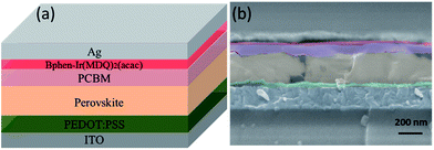 |
| | Fig. 1 (a) Device architecture of perovskite solar cells employing a Bphen:Ir(MDQ)2(acac) interlayer. (b) Cross-sectional SEM image of the PSC. | |
Measurements and characterization
Steady-state photo-luminescence (PL) measurements were acquired using a Horiba spectrofluorometer (Fluoromax-4) with a 500 nm excitation wavelength at room temperature. The UV-Vis absorption spectra were collected using a Shimadzu spectrophotometer (mode UV2450). The current density–voltage (J–V) characteristics of the PSC devices were measured under AM 1.5 G solar irradiation at 100 mW cm−2 (Newport, Class AAA solar simulator, 94023A-U). Scanning electron microscopy (SEM) images were obtained using a field emission scanning electron microscope (Hitachi SU8010). Atomic force microscopy (AFM) images were measured using a Dimension-Icon (Bruker). Electrochemical impedance spectroscopy (EIS) was investigated using an IM6e Electrochemical Workstation (ZAHNER, Germany) with an alternating current amplitude of 10 mV. The impedance spectra were recorded in the frequency range of 100 kHz to 0.01 kHz, and the equivalent electrical circuit was fitted using the impedance data.
Results and discussion
Photovoltaic performance
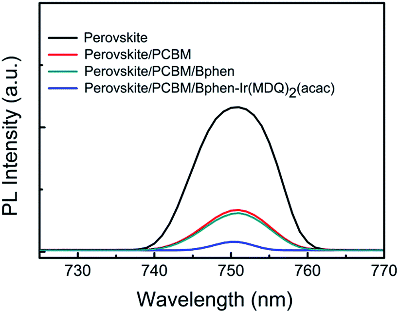
The role of Bphen:Ir(MDQ)2(acac) as a modification layer is confirmed in the planar heterojunction PSCs. The charge transfer responses between the perovskite and the corresponding interface layer were determined using PL measurements. Fig. 2 shows the PL spectra of perovskite, perovskite/PCBM, perovskite/PCBM/Bphen, and perovskite/PCBM/Bphen:Ir(MDQ)2(acac) thin films. The emission peak of the pristine perovskite film is observed at 750 nm. When the perovskite layer is coated with PCBM or PCBM/Bphen, there is a striking quenching effect. This suggests that Bphen could act as an efficient interfacial layer for electron transport. Particularly, the PL intensity of the film is seriously quenched after being coated with PCBM/Bphen:Ir(MDQ)2(acac). The striking quenching phenomenon illustrates that there is more efficient charge transfer between them.21,30
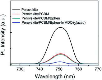 |
| | Fig. 2 Photoluminescence response for a CH3NH3PbI3−xClx perovskite film and those coated with PCBM, PCBM/Bphen, and PCBM/Bphen-Ir(MDQ)2(acac) thin films. | |
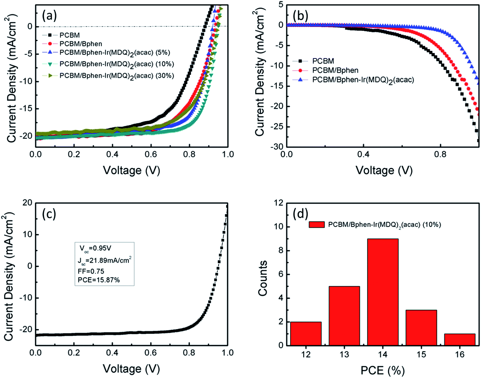
To study the effect of Bphen:Ir(MDQ)2(acac) as the cathode interface modification layer on device performance, the current density–voltage (J–V) characteristics of the planar PSCs (Fig. 3) were measured under AM 1.5 G illumination (100 mW cm−2) in air. The performance parameters of the devices are summarized in Table 1. Compared with the reference planar PSC (a Voc of 0.88 V, short-circuit current density (Jsc) of 20.06 mA cm−2, fill factor (FF) of 0.59 and PCE of 10.77%), the performance of the solar cells is much enhanced after the insertion of Bphen or Bphen:Ir(MDQ)2(acac) between PCBM and the Ag electrode. Analyzing the data, it can be seen that the FF and PCE values have been obviously enhanced. It is worth noting that the device based on a Bphen:Ir(MDQ)2(acac) interfacial layer exhibits a Voc of 0.94 V, a very high FF of 0.74 and thus yields an average PCE of 14.35%. Fig. 3a presents different doping ratios of Ir(MDQ)2(acac) in Bphen and the performance of the devices. It is concluded that a 10 wt% doping ratio could achieve the best PCE of the devices in Table 1.
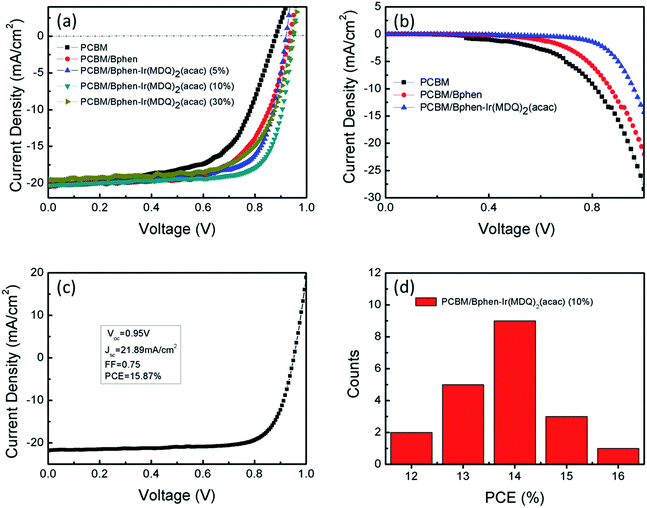 |
| | Fig. 3 (a) Current–voltage characteristics of the PSCs with different modification layers under illumination of AM 1.5 G, 100 mW cm−2. (b) J–V characteristics measured in the dark. (c) The J–V curve of the PSC with the best efficiency. (d) Histogram of PCEs measured from 20 devices with Bphen:Ir(MDQ)2(acac). | |
Table 1 Photovoltaic parameters of perovskite devices with different modification layers
| Devices |
V
oc (V) |
J
sc (mA cm−2) |
FF |
PCE (%) |
R
s (Ω cm2) |
R
sh (Ω cm2) |
| PCBM |
0.88 |
20.06 |
0.59 |
10.77 |
11.49 |
263.97 |
| PCBM/Bphen |
0.93 |
20.15 |
0.65 |
12.23 |
5.11 |
297.74 |
| PCBM/Bphen-Ir(MDQ)2(acac) (5%) |
0.92 |
20.38 |
0.71 |
13.21 |
3.21 |
512.45 |
| PCBM/Bphen-Ir(MDQ)2(acac) (10%) |
0.94 |
20.28 |
0.74 |
14.35 |
3.07 |
574.45 |
| PCBM/Bphen-Ir(MDQ)2(acac) (30%) |
0.93 |
19.55 |
0.67 |
12.38 |
4.80 |
438.66 |
To further understand the influence of the interlayer of Bphen:Ir(MDQ)2(acac) on the photovoltaic efficiency of PSCs, the J–V characteristics of the 10 wt% doping ratio device were recorded in the dark. Fig. 3b shows that the current remains similar at a small reverse bias while it increases dramatically with the enhancement of the bias voltage. The difference in the dark J–V characteristics is associated with the different interlayer modification effects. The slowest growing curve of the Bphen:Ir(MDQ)2(acac) based device means the smallest dark current. This reflects that the recombination rate between the Ag electrode and perovskite/PCBM is suppressed by introducing Bphen:Ir(MDQ)2(acac). This is consistent with the previous report regarding increased shunt resistance (Rsh).31 In addition, both Bphen and Bphen:Ir(MDQ)2(acac) improve the current injection under the forward bias (Fig. S1†), but the Bphen:Ir(MDQ)2(acac) based device produces an even better diode behavior than the Bphen based one. The relatively larger injection current at a forward bias in the Bphen:Ir(MDQ)2(acac) based device agrees well with the lower Rs. It is assumed that the Bphen:Ir(MDQ)2(acac) interlayer induces a good interface contact between perovskite/PCBM and the Ag electrode resulting in the significant reduction of Rs. As a matter of fact, we can obtain a champion device with a PCE of 15.87%, Voc of 0.95 V, Jsc of 21.89 mA cm−2, and FF of 0.74 in Fig. 3c. To determine the variation trend of the device performance, 20 devices were measured to plot a corresponding histogram of PCEs. Fig. 3d indicates that the Bphen:Ir(MDQ)2(acac) based devices have higher PCEs than the reference devices (Fig. S2†). Meanwhile, the device exhibits a lower hysteresis (Fig. S3†).
Fig. 4 displays the UV-Vis spectra of the perovskite layer covered with PCBM and PCBM/Bphen:Ir(MDQ)2(acac) layers. There is no large difference in the absorption profiles of the perovskite films coated with PCBM and PCBM/Bphen:Ir(MDQ)2(acac). The variation of Jsc values in Table 1 also reflects the same tendency. Although the doping of Ir(MDQ)2(acac) hardly changes the absorption and the Jsc, a compact interface contact is assumed to be formed between PCBM and the Ag electrode by inserting the Bphen:Ir(MDQ)2(acac) interfacial layer. This fact is favorable for the suppression of shunting paths in the device and benefits the electron extraction, resulting in an enhanced FF and PCE.
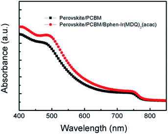 |
| | Fig. 4 UV-Vis absorption spectra of perovskite films coated with PCBM and Bphen:Ir(MDQ)2(acac) interlayers. | |
Cathode interface evaluations
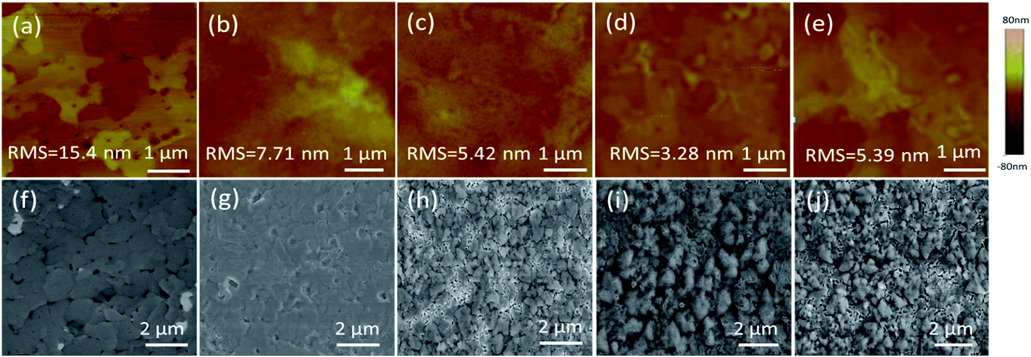
A uniform morphology forming a good interface contact between the films and the top electrode plays a key role in device performance. Fig. 5a–e show the surface textures of the perovskite layer with and without PCBM or PCBM/Bphen, Bphen:Ir(MDQ)2(acac) layers obtained using atomic force microscopy (AFM) in tapping mode (scan area 5 μm × 5 μm). Fig. 5a shows a root-mean-square roughness (RMS) of 15.4 nm for the pure perovskite layer. After coating with PCBM, the surface morphology dramatically decreases to 7.71 nm (Fig. 5b). After further deposition of Bphen (Fig. 5c) or Bphen:Ir(MDQ)2(acac) (10 wt%) (Fig. 5d), a smoother surface is obtained; especially for the latter, with the RMS reduced to 3.28 nm from 5.42 nm. Nevertheless, a higher doping concentration of Ir(MDQ)2(acac) (30 wt%) results in an increase of RMS (5.39 nm). A PCBM covering leads to a homogeneous surface morphology compared with the pristine perovskite film. Further coating of the Bphen:Ir(MDQ)2(acac) layer effectively fills the voids in the coated PCBM surface. The contact interface between perovskite and the Ag electrode is smoother and more compact, greatly reducing the contact resistance on the Ag electrode side. In addition, insertion of Bphen and Bphen:Ir(MDQ)2(acac) can fill the voids in the perovskite/PCBM film. The good coverage of the interlayer on the perovskite/PCBM film can block the direct contact between the cathode and PCBM, and thus minimize current leakage. It should be noted that excess doping of Ir(MDQ)2(acac) leads to the formation of a cluster in the Bphen:Ir(MDQ)2(acac) film. The cluster would harm the smoothness of the film surface and thus deteriorate the device performance. SEM evaluations were further carried out to elucidate the influence of the Bphen:Ir(MDQ)2(acac) interlayer. As shown in Fig. 5f and g, sharply faceted crystalline domains are formed and the nanocrystals are connected in the perovskite film with poor surface coverage, even if PCBM is coated. The voids in the active layer result in low resistance shunting paths in solar cells, and then reduce the FF. When the perovskite films are coated with PCBM/Bphen (Fig. 5h) or PCBM/Bphen:Ir(MDQ)2(acac) (Fig. 5i), the voids are filled and the film becomes denser and smoother, which is well matched with the results of AFM. The compact structure of the films is beneficial to reduce current leakage, which decreases the probability of carrier recombination. Moreover, it is found that some clusters appear on the surface of the film in cases of excess doping of Ir(MDQ)2(acac) (Fig. 5j), which results in a rough surface and has a detrimental side effect on the device performance, which is consistent with the results in Fig. 3a and Table 1.
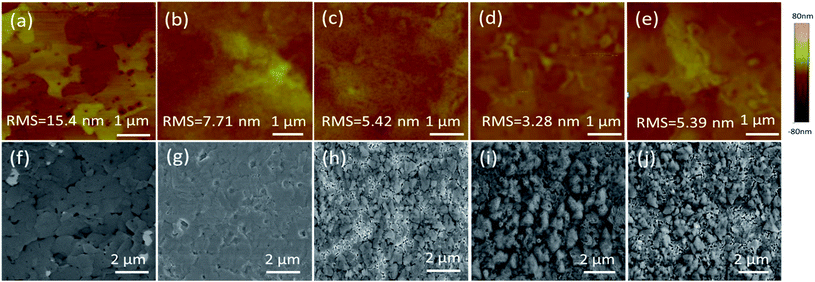 |
| | Fig. 5 AFM images (5 μm × 5 μm) of (a) perovskite film and (b) perovskite/PCBM film, (c) perovskite/PCBM/Bphen film, (d) perovskite/PCBM/Bphen:Ir(MDQ)2(acac) (10 wt%) and (e) perovskite/PCBM/Bphen:Ir(MDQ)2(acac) (30 wt%). The root-mean-square roughness (RMS) is indicated on the AFM images. SEM images of (f) perovskite film and that coated with (g) PCBM, (h) PCBM/Bphen, (i) PCBM/Bphen:Ir(MDQ)2(acac) (10 wt%) and (j) PCBM/Bphen:Ir(MDQ)2(acac) (30 wt%). | |
Fig. 6 presents the electrochemical impedance spectra (EIS) of the PSCs with different cathode interfacial layers under dark conditions. The equivalent electrical circuit is fitted using the impedance data. The internal series resistance (Rs) is composed of the sheet resistance (Rsr) of the electrodes, and the charge transfer resistance (RCT) inside the perovskite thin film and at the interface of the perovskite/electron transporting layer. The Rs in the Bphen and Bphen:Ir(MDQ)2(acac)-based PSCs is 37 Ω cm2 and 32 Ω cm2, respectively, which are lower than the 65.9 Ω cm2 in the reference device without any interfacial layers. Insertion of Bphen:Ir(MDQ)2(acac) provides a good interface contact between the perovskite/electron transporting layer and the Ag electrode, which greatly decreases the Rs. The variation trend is consistent with the above mentioned J–V characteristics. Rs is lower in Bphen and Bphen:Ir(MDQ)2(acac)-based PSCs, which is associated with the smoother and more compact cathode interface contact. EIS evaluation further verified the excellent role of Bphen:Ir(MDQ)2(acac) as a cathode interfacial layer in planar PSCs.
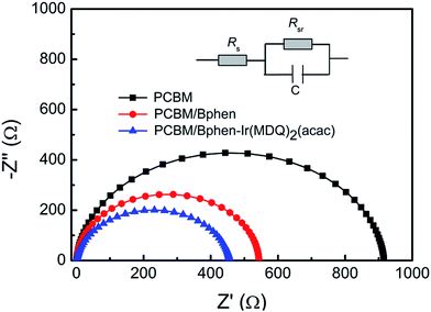 |
| | Fig. 6 Nyquist plots at V = Voc for PSCs. EIS was measured in the dark and the equivalent electrical circuit is shown. | |
Conclusion
In summary, a doped material, Bphen:Ir(MDQ)2(acac), has been employed as a cathode interfacial layer to improve the cathode interface contact between perovskite/PCBM and an Ag electrode in planar PSCs. The device performance is largely improved with a champion PCE of 15.87% and an average PCE of 14.35% in comparison with the average PCE of 10.77% for the reference device without an interfacial layer. The enhanced FF (from 0.59 to 0.74) is ascribed as the main factor for the improved cell efficiency. Cathode interface evaluations revealed that a compact and smooth interface contact between perovskite/PCBM and the Ag top electrode is formed by inserting Bphen:Ir(MDQ)2(acac) in the device. A flat interface is beneficial for reducing current leakage, which decreases the probability of carrier recombination, resulting in an enhanced FF and thus improved device efficiency. Our finding provides a simple and efficient method for interfacial modification in planar perovskite solar cells.
Acknowledgements
We acknowledge financial support from the Scientific Research Foundation, the “973 Program—the National Basic Research Program of China” Special Funds for the Chief Young Scientist (2015CB358600), the Excellent Young Scholar Fund from National Natural Science Foundation of China (21422103), the Natural Science Foundation of China (61307037), Jiangsu Fund for Distinguished Young Scientist (BK20140010), the Priority Academic Program Development of Jiangsu Higher Education Institutions (PAPD), and Jiangsu Scientific and Technological Innovation Team (2013).
References
- H. J. Feng, T. R. Paudel, E. Y. Tsymbal and X. C. Zeng, J. Am. Chem. Soc., 2015, 137, 8227–8236 CrossRef CAS PubMed.
- M. Z. Liu, B. M. Johnston and H. J. Snaith, Nature, 2013, 501, 395–403 CrossRef CAS PubMed.
- P. Gao, M. Grätzel and M. K. Nazeeruddin, Energy Environ. Sci., 2014, 7, 2448–2463 CAS.
- S. D. Stranks, G. E. Eperon, G. Grancini, C. Menelaou, M. J. P. Alcocer, T. L. Laura, M. Herz, A. Petrozza and H. J. Snaith, Science, 2013, 342, 341–344 CrossRef CAS PubMed.
- G. C. Xing, N. Mathews, S. Y. Sun, S. S. Lim, Y. M. Lam, M. Grätzel, S. Mhaisalkar and T. C. Sum, Science, 2013, 342, 344–347 CrossRef CAS PubMed.
- A. Kojima, K. Teshima, Y. Shirai and T. Miyasaka, J. Am. Chem. Soc., 2009, 131, 6050–6051 CrossRef CAS PubMed.
- H. S. Kim, C. R. Lee, J. H. Im, K.-B. Lee, T. Moehl, A. Marchioro, S. J. Moon, R. Humphry-Baker, J. H. Yum, J. E. Moser, M. Graetzel and N. G. Park, Sci. Rep., 2012, 2, 591–600 Search PubMed.
- M. M. Lee, J. Teuscher, T. Miyasaka, T. N. Murakami and H. J. Snaith, Science, 2012, 338, 643–647 CrossRef CAS PubMed.
- Z. L. Ku, Y. G. Rong, M. Xu, T. F. Liu and H. W. Han, Sci. Rep., 2013, 3, 3132–3137 Search PubMed.
- H. Zhou, Q. Chen, G. Li, S. Luo, T. b. Song, H. S. Duan, Z. Hong, J. You, Y. Liu and Y. Yang, Science, 2014, 345, 542–546 CrossRef CAS PubMed.
- N. J. Jeon, J. H. Noh, W. S. Yang, Y. C. Kim, S. Ryu, J. Seo and S. I. Seok, Nature, 2015, 517, 476–480 CrossRef CAS PubMed.
- G. E. Eperon, V. M. Burlakov, P. Docampo, A. Goriely and H. J. Snaith, Adv. Funct. Mater., 2014, 24, 151–157 CrossRef CAS.
- X. Gong, M. Li, X. B. Shi, H. Ma, Z. K. Wang and L. S. Liao, Adv. Funct. Mater., 2015, 25, 6671–6678 CrossRef CAS.
- L. Yan, Y. Song, Y. Zhou, B. Song and Y. Li, Org. Electron., 2015, 17, 94–101 CrossRef CAS.
- H. Zhang, Y. Shi, F. Yan, L. Wang, K. Wang, Y. Xing, Q. Dong and T. Ma, Chem. Commun., 2014, 50, 5020–5022 RSC.
- Y. H. Deng, E. Peng, Y. C. Shao, Z. G. Xiao, Q. F. Dong and J. S. Huang, Energy Environ. Sci., 2015, 8, 1544–1550 CAS.
- J. H. Im, J. Luo, M. Franckevičius, N. Pellet, P. Gao, T. Moehl, S. M. Zakeeruddin, M. K. Nazeeruddin, M. Grätzel and N. G. Park, Nano Lett., 2015, 15, 2120–2126 CrossRef CAS PubMed.
- L. F. Zhu, J. J. Shi, S. T. Lv, Y. Y. Yang, X. Xu, Y. Z. Xu, J. Y. Xiao, H. J. Wu, Y. H. Luo, D. M. Li and Q. B. Meng, Nano Energy, 2015, 15, 540–548 CrossRef CAS.
- M. Qian, M. Li, X. B. Shi, H. Ma, Z. K. Wang and L. S. Liao, J. Mater. Chem. A, 2015, 3, 13533–13539 CAS.
- Z. H. Wei, H. Chen, K. Y. Yan and S. H. Yang, Angew. Chem., 2014, 126, 13455–13459 CrossRef.
- Z. W. Wu, S. Bai, J. Xiang, Z. C. Yuan, Y. G. Yang, W. Cui, X. Y. Gao, Z. Liu, Y. Z. Jin and B. Q. Sun, Nanoscale, 2014, 6, 10505–10510 RSC.
- J. Y. Jeng, K. C. Chen, T. Y. Chiang, P. Y. Lin, T. D. Tsai, Y. C. Chang, T. F. Guo, P. Chen, T. C. Wen and Y. J. Hsu, Adv. Mater., 2014, 26, 4107–4133 CrossRef CAS PubMed.
- J. Seo, S. Park, Y. C. Kim, N. J. Jeon, J. H. Noh, S. C. Yoon and S. Seok, Energy Environ. Sci., 2014, 7, 2642–2646 CAS.
- Q. Xue, Z. Hu, J. Liu, J. Lin, C. Sun, Z. Chen, C. Duan, J. Wang, C. Liao, W. M. Lau, F. Huang, H.-L. Yip and Y. Cao, J. Mater. Chem. A, 2014, 2, 19598–19603 CAS.
- X. D. Liu, H. Yu, L. Yan, Q. Q. Dong, Q. Wan, Y. Zhou, B. Song and Y. F. Li, ACS Appl. Mater. Interfaces, 2015, 7, 6230–6237 CAS.
- X. B. Shi, C. H. Gao, D. Y. Zhou, M. Qian, Z. K. Wang and L. S. Liao, Appl. Phys. Express, 2012, 5, 102102–102107 CrossRef.
- L. Ding, Y. Q. Sun, H. Chen, F. S. Zu, Z. K. Wang and L. S. Liao, J. Mater. Chem. C, 2014, 2, 10403–10408 RSC.
- Y. H. Lou, Z. K. Wang, S. Naka and H. Okada, Appl. Phys. Lett., 2011, 99, 033305–033307 CrossRef.
- Z. K. Wang, M. Li, D. X. Yuan, X. B. Shi, H. Ma and L. S. Liao, ACS Appl. Mater. Interfaces, 2015, 7, 9645–9651 CAS.
- S. S. Li, K. H. Tu, C. C. Lin, C. W. Chen and M. Chhowalla, ACS Nano, 2010, 4, 3169–3174 CrossRef CAS PubMed.
- H. Zhang, H. Azimi, Y. Hou, T. Ameri, T. Przybilla, E. Spiecker, M. Kraft, U. Scherf and C. J. Brabec, Chem. Mater., 2014, 26, 5190–5193 CrossRef CAS.
Footnote |
| † Electronic supplementary information (ESI) available: The current density–voltage (J–V) characteristics of planar PSCs were measured under forward bias in the dark. Corresponding histogram of PCEs measured from PSCs devices with different doping ratios. J–V curves of PSCs with different scan directions. See DOI: 10.1039/c5ta09231k |
|
| This journal is © The Royal Society of Chemistry 2016 |
Click here to see how this site uses Cookies. View our privacy policy here.