
Enhancing the crystallization and optimizing the orientation of perovskite films via controlling nucleation dynamics†
Qiuju
Liang
ab,
Jiangang
Liu
ab,
Zhongkai
Cheng
ab,
Yan
Li
ab,
Liang
Chen
ab,
Rui
Zhang
ab,
Jidong
Zhang
ab and
Yanchun
Han
*ab
aState Key Laboratory of Polymer Physics and Chemistry, Changchun Institute of Applied Chemistry, Chinese Academy of Sciences, 5625 Renmin Street, Changchun 130022, P. R. China
bUniversity of the Chinese Academy of Sciences, No. 19A Yuquan Road, Beijing 100049, P. R. China. E-mail: ychan@ciac.ac.cn; Fax: +86-431-85262120; Tel: +86-431-85262120
First published on 13th November 2015
Abstract
The morphology of the active layer is at the heart of perovskite solar cells. It is deeply related to charge transport and extraction, which depend on coverage ratio, crystallinity, crystal size and perhaps crystal orientation. However, the crystallization process in a solution-processed perovskite film is ungovernable and there is no clear guideline for how to improve the film morphology. Here, we employed the selective solvent annealing (SSA) method to control crystallization kinetics, producing a flat CH3NH3PbIxCl3−x film with almost full coverage, micron scale grain size, enhanced crystallinity and optimized crystal orientation. The improved morphology is attributed to the formation of a uniformly distributed nucleus of perovskite before thermal annealing, resulting from the selective solubility of selective solvents, which accelerates the crystallization of lead iodide (PbI2) and the intercalation of methylammonium iodide (MAI) into the PbI2 crystal lattice. Furthermore, driven by thermodynamics, the nucleus tends to rearrange during the thermal annealing process, and thus the crystal orientation turns from (h k 0) (h = k) to (h 0 0) orientation, which enables the corner of the inorganic framework to come into contact with the substrate. The enhanced crystallinity, enlarged crystal size and optimized crystal orientation are beneficial for the carrier collection due to the prolonged carrier life time and reduced carrier recombination, which resulted in the highest power conversion efficiency (PCE) of 12.38%, about 37% increase compared with the reference device.
Introduction
Low fabrication cost, ease of processing (solution processing), and excellent light-harvesting characteristics make perovskite materials currently among the most competitive candidates for thin-film photovoltaic (PV) applications.1 Since organometal halide perovskites were first used as sensitizers in solar cells, solution-processed hybrid perovskite solar cells have now achieved a remarkably high photovoltaic power conversion efficiency of 20.1%, which have already reached the commercial requirement of high efficiency.2–5As is well known, the morphology of perovskite films is very crucial to device performance.6–8 However, solution-processed films usually suffer from low film coverage ratio, small grain size and low crystallinity due to the uncontrollable crystallization process which are detrimental to device performance, such as light absorption, carrier transport and collection.9–12 It is recently reported that the crystallization process is sensitive to interfacial energy, solvent choice, deposition temperature, etc. Therefore, controlling the nucleation and crystallization process during film deposition and annealing is an attractive route to improve perovskite film morphology.13–15 Cheng et al. reported an effective way to promote the nucleation via spin-coating poor solvents onto perovskite wet films to improve the perovskite film morphology. The poor solvent would extract the main solvent and condense the solution on the substrate, which impelled the precursor solutes to nucleate, forming a highly uniform film with enhanced crystallinity.16 Similarly, the introduction of chloridion could also facilitate the nucleation process, which functioned as heterogeneous nucleation sites and enhanced the nucleus density of the perovskite film, resulting in a perfect morphology.14,17,18 In addition, regulating the crystal growth process could also improve the film morphology. Adding solvents with the coordination effect with lead ions into the precursor solution could slow down the crystallization process due to the formation of “coordinated intermediate phase”, which encouraged homogeneous nucleation and obtained a continuous perovskite film.19,20 Using good solvents to treat the perovskite film during the thermal annealing process is also an effective method.21 It promoted the diffusion of precursors during the crystal growth which resulted in a large perovskite grain size.
Besides film quality, the crystal orientation may also have profound influence on device performance. As we know, perovskite is a typical kind of organic–inorganic hybrid material, in which an extended framework is formed by the iodide ions (I−) and lead ions (Pb2+) by strong ionic or covalent interactions, while the organic component intercalates into the framework through van der Waals forces.22 Thus, there are many types of contacts between the perovskite and substrate interface. For the (100) direction, the corner of the inorganic framework would make contact at the perovskite/substrate interface, while for the (110) direction, the inorganic framework represents the edge contact at the interface. The different contacts at the interface may affect the charge extraction and collection. However, as far as we know, perovskite crystals processed by the solution-processing technique usually exhibit strong (h k 0) (h = k) preferred orientation.
In this manuscript, we developed a simple and effective strategy, selective solvent annealing (SSA), to optimize the morphology and orientation of the CH3NH3PbI3−xClx film by controlling the nucleation process. A selective solvent, isopropanol (IPA), acts as a good solvent for MAI but as a poor solvent for PbX2 (X = Cl or I). The selective solubility results in a high degree of supersaturation of Pb2+ and X−, thus favoring the precipitation and crystallization of lead halide. Meanwhile, IPA forms H-bonding with MAI, which could assist the intercalation of MA+ into the lead halide crystal lattice, ultimately forming a uniform and dense perovskite crystal nucleus. The formation of the nucleus would avoid the slow nucleation process, resulting in flat perovskite films with enlarged grain size and enhanced crystallinity. In addition, the nucleus tends to rearrange via the Ostwald ripening process to attain thermodynamic stability during the thermal annealing process, promoting the crystal orientation to transform into the (h 0 0) orientation. The improved film morphology and orientation would facilitate the carrier collection due to the prolonged carrier life time and reduced carrier recombination, leading to a remarkable increase of device performance.
Experimental
Materials
Methylammonium iodide (MAI) and lead chloride (PbCl2) were purchased from Yingkou Optimal Choice Trade, China. [6,6]-Phenyl-C61-butyric acid methyl was purchased from American Dye Source. The bis-functional of C70 (C70-bis) was purchased from 1-Material, Canada. N,N-Dimethylformamide (DMF) was purchased from Aldrich company. Isopropanol (IPA) and toluene (TOL) were purchased from Beijing Chemical Factory, China. The materials were used without further purification.Solvent vapor annealing
During the solvent vapor annealing process, the active layer was placed into a glass tube which contained toluene, isopropanol and DMF at the bottom, respectively. Stable vapor gradient along the tube could be obtained after 15 min since the liquid solvent location was fixed. The vapor pressure of the sample was P = 0.54 (25 °C). (The length of the tube is 3 cm and the liquid height is 0.2 cm. The solvent vapor pressure P is given by P = L/L0, where L is the distance from the up edge of the setup to the specimen position and L0 is the length given by the distance from the up edge of the setup to the surface of the solvent at the bottom of the tube). The samples of toluene, isopropanol and DMF were treated under this vapor pressure for 180 s, 120 s and 20 s, respectively, as the active layer was spin-coated.Fabrication of thin-film perovskite solar cells
The devices were fabricated in the configuration of indium tin oxide (ITO)/PEDOT:PSS/CH3NH3PbI3−xClx/[6,6]-phenyl-C61-butyric acid methyl ester (PC61BM)/fullerene surfactant (C70-bis)/Al. The ITO glass substrates were cleaned sequentially with detergent and deionized water, acetone, and isopropanol under sonication for 10 min. After drying under a nitrogen flow, substrates were treated with UV-ozone for 25 min. The poly(ethylenedioxythiophene):poly(styrenesulfonate) (PEDOT:PSS, Baytron P4083, filtered through a 0.45 μm nylon filter) layer was first spin-coated at 5k rpm for 40 s on this well-cleaned ITO glass and dried at 140 °C in a vacuum for 30 min. The substrates were transferred into a N2-filled glovebox, where the thin-film perovskite layers were spin-coated from a homogeneous 30 wt% (PbCl2![[thin space (1/6-em)]](https://www.rsc.org/images/entities/char_2009.gif) :MAI with a molar ratio of 1:3 in DMF) precursor solution at 7k rpm for 45 s (300 nm thickness) on the hot substrates (about 63 °C) and then annealed at 75 °C for 5 h. Afterward, the PC61BM (15 mg mL−1 in chloroform) and C70-bis surfactant (2 mg mL−1 in isopropyl alcohol) were then sequentially deposited by spin coating at 3k rpm for 60 s, respectively. Finally, a layer structure of Al (90 nm) was deposited at the top of the active layer by thermal evaporation in a vacuum of 2 × 10⁻⁴ Pa to complete the device fabrication.
:MAI with a molar ratio of 1:3 in DMF) precursor solution at 7k rpm for 45 s (300 nm thickness) on the hot substrates (about 63 °C) and then annealed at 75 °C for 5 h. Afterward, the PC61BM (15 mg mL−1 in chloroform) and C70-bis surfactant (2 mg mL−1 in isopropyl alcohol) were then sequentially deposited by spin coating at 3k rpm for 60 s, respectively. Finally, a layer structure of Al (90 nm) was deposited at the top of the active layer by thermal evaporation in a vacuum of 2 × 10⁻⁴ Pa to complete the device fabrication.
Characterization
The morphology of hybrid perovskite films was acquired by field-emission scanning electron microscopy (FESEM) using a Micro FEI Philips XL-30-ESEMFEG microscope at an accelerating voltage of 20 kV. The sample was sputter coated with gold before SEM observation. The elemental distribution of the film was analyzed using energy dispersive spectroscopy (EDS, GENESIE 2000-EDAX).The crystallinity of the perovskite film was analyzed using out-of-plane grazing incidence X-ray diffraction (GIXD) measurements, two-dimensional GIXD (2D GIXD). The GIXD profiles were obtained by using a Bruker D8 Discover reflector with an X-ray generation power of 40 kV tube voltage and 40 mA tube current. The measurements were achieved in a scanning interval of 2θ between 3 and 60°. The 2D GIXD profiles were obtained by using a Rigaku Smartlab instrument with an X-ray generation power of 40 kV tube voltage and 30 mA tube current and BL14B1 at Shanghai Synchrotron Radiation Facility (SSRF; λ = 0.124 nm).
The photon absorption of the active layer and situ absorption spectrum was recorded by combining UV-vis absorption spectroscopy (Shimadzu UV 3600 spectrophotometer in a spectral range of 300–1000 nm) with a home-made heater.
To demonstrate the orientation evolution, situ 2D GIXD was operated through combining Rigaku SmartLab instrument with an X-ray generation power of 40 kV tube voltage and 30 mA tube current with a home-made heater. The perovskite film without solvent vapor treatment was annealed at 65 °C and the film with solvent vapor treatment was annealed at 75 °C under vacuum.
Current density–voltage (I–V) characteristics of the PV cells were measured using a computer controlled Keithley 236 source meter under AM1.5G illumination from a calibrated solar simulator with an irradiation intensity of 100 mW cm−2. The device area was 12 mm2, determined by the overlap of the cathode and anode. An aperture size of 10.6 was used to define the light absorption area, which would avoid the overestimation of the photocurrent density by the optical pining effect.23
Nanosecond fluorescence lifetime experiments were performed using the time-correlated single-photon counting (TCSPC) system under right-angle sample geometry. A 400 nm picosecond diode laser (Edinburgh Instruments EPL375, repetition rate 20 MHz) was used to excite the samples. The fluorescence was collected by using a photomultiplier tube (Hamamatsu H5783p) connected to a TCSPC board (Becker & Hickl SPC-130). The time constant of the instrument response function (IRF) is about 220 ps.
Results and discussion
Selective solvent (IPA) annealing (SSA) was employed to improve the morphology and orientation of perovskite films. Due to the accelerated nucleation dynamics during the SSA process and the crystal fusion during the thermal annealing process, a uniform and high crystallized perovskite film with (h 0 0) orientation was obtained, which is beneficial for the device performance.Increasing the film coverage and grain size by regulating the nucleation and crystal growth process
Recently, it has been reported that the uncontrollable nucleation kinetics usually lead to poor morphology of the perovskite film fabricated by the solution-processing technique.19,24,25 Here, we employed the SSA method to control the nucleation and crystal growth kinetics, and finally obtained a continuous film with large grain size and enhanced crystallinity.Fig. 1 shows the scanning electron microscopy (SEM) images of the pristine film and the film treated by SSA (treated film). As we can see, the pristine film contains many pin-holes and the crystal size is less than 200 nm as shown in Fig. 1(A) and (a), which is caused by the high boiling point (153 °C) and slow evaporation of DMF.15 While the treated film exhibits almost full surface coverage with micron-sized grains, which pack in a dense manner as shown in Fig. 1(B) and (b) (the optimization of different annealing times is shown in Fig. S1†).
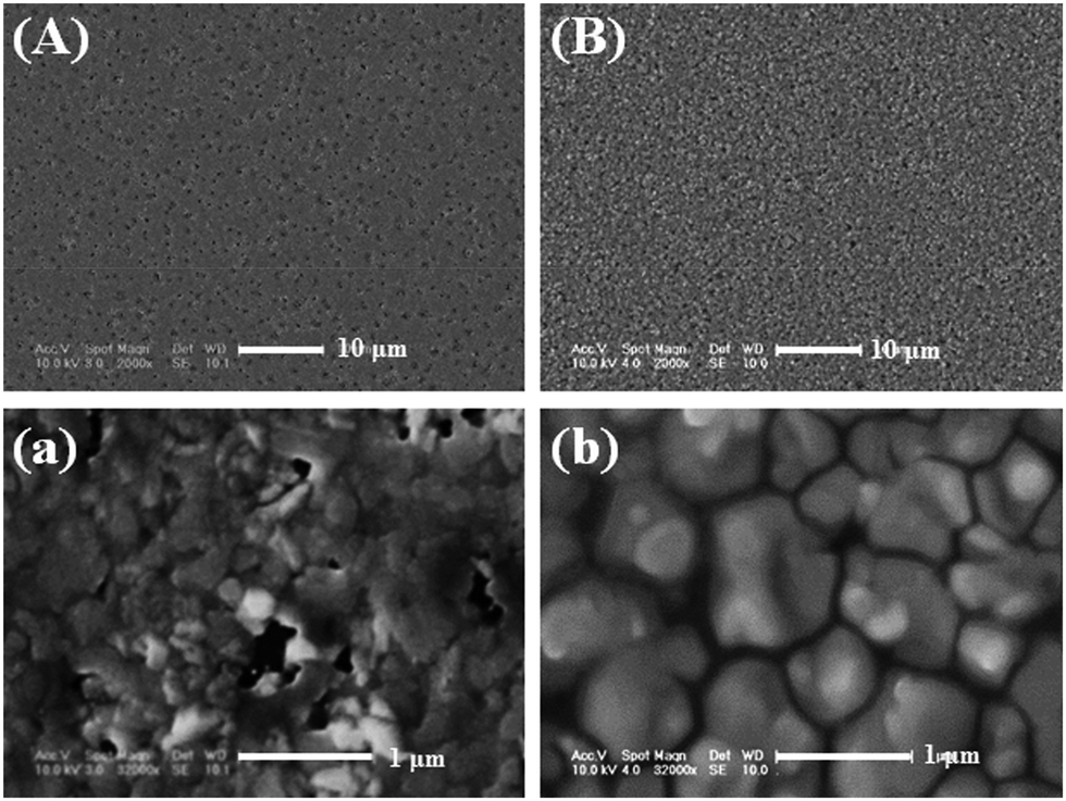 | ||
| Fig. 1 Low-magnification and high-magnification SEM top-view images of the perovskite film with and without SSA treatment: (A) and (a) without SSA treatment; (B) and (b) film with SSA treatment. All the films are thermally annealed for 5 h at 75 °C. | ||
The improved film morphology could be attributed to the regulated nucleation process due to the SSA treatment. In order to testify the effects of IPA vapor on the nucleation process, we vacuumized the films treated by IPA vapor for different times immediately to freeze its morphology. As shown in Fig. 2, the as spin-coated film without annealing (0 s) is a uniform flat film, and it was composed of lead halide and the coordinated Pb2+–N,N-dimethylformamide (DMF) compound, which can be confirmed by XRD (Fig. S2A†).20 While some distinct changes were gradually observed with the extended annealing time: at first, small regular cubes appear and its number increases gradually (30–120 s), the cubes are perovskite crystals as confirmed by XRD as shown in Fig. S2A;† subsequently, the cubes get bigger and some spherical aggregates appear on the top of the film (150–210 s), which are formed by MAI deduced by energy dispersive spectroscopy (EDS) results (Fig. S2B†). Based on these phenomena mentioned above, we supposed the changes stem from the special function of IPA. First, due to the low solubility to lead halide, IPA would inhibit the coordination between Pb2+ and DMF molecules and promote the crystallization of lead halide. In addition, H-bonding could be formed between MA+ and IPA, which promotes the intercalation of MA+ into lead halide to form a perovskite nucleus owing to the small molecular size and ease of volatilization of IPA. If the film was over exposed to IPA vapor (>150 s), MAI would form large aggregates. The aggregates inhibited the MA+ from intercalating into an inorganic framework, and led to an incomplete coverage morphology as shown in Fig. S1.† To sum up, the appropriate annealing time is 120 s, which could promote the formation of a uniform and dense perovskite nucleus, a precondition to form a continuous film.
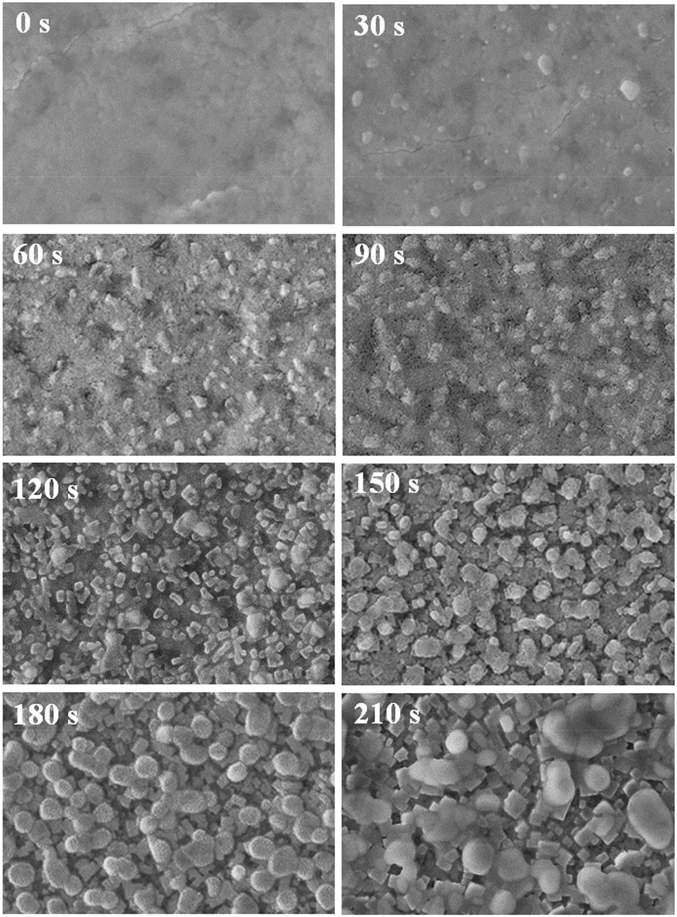 | ||
| Fig. 2 SEM top-view images of the perovskite film with SSA treatment for different times. All the films were placed under vacuum for 2 hours without thermal annealing. | ||
To further explore the underlying nucleation crystal growth kinetics mechanism, time dependence of UV-vis absorption spectra (In situ UV-vis absorption spectra) during the thermal annealing process was studied (shown in Fig. 3). Compared with the spectrum of the pristine film (Fig. 3A), the spectrum of the treated film (Fig. 3B) is broader and its eventual absorption intensity is stronger, which means an enhanced crystallinity of perovskite after the SSA. In order to quantify the change of the crystallization process during thermal annealing treatment, we tracked the peak intensity variances at 730 nm (Iincrease) against the time (t), of which the absorbance corresponds to the amount and size of perovskite crystals in films.26 As shown in Fig. 3a, the crystallization starts from a relatively slow nucleation process (0–112 min), followed by a rapid growth process (112–256 min), and their corresponding rates are kpn = 2.8 × 10⁻⁴ and kpc = 1.25 × 10⁻³, respectively.14 For the treated film, the whole crystallization process is shortened to 128 min as shown in Fig. 3b. Its nucleation process lasts about 72 min (kpn = 0) and the crystal growth process lasts about 50 min (ksc = 3.0 × 10⁻³), which are faster than the pristine film. It is worth noting that the kpn for the treated film is 0 and the absorption intensity for the nucleus is about 0.09 (the corresponding absorption intensity for the pristine film is 0.05). It means that a mass of nucleus has already been formed during the SSA process, which is an important precondition for forming a uniform perovskite film. Due to the existing nucleus, the gradual formation of the nucleus during thermal annealing would be avoided, which tends to result in a poor morphology of the perovskite film.27 In addition, the faster crystal growth rate of the treated film indicates that the formed nucleus favors the crystal growth. The faster transition of the perovskite reduces the processing time which makes it easier for fabrication as well as saves the energy during the manufacture of solar cells.
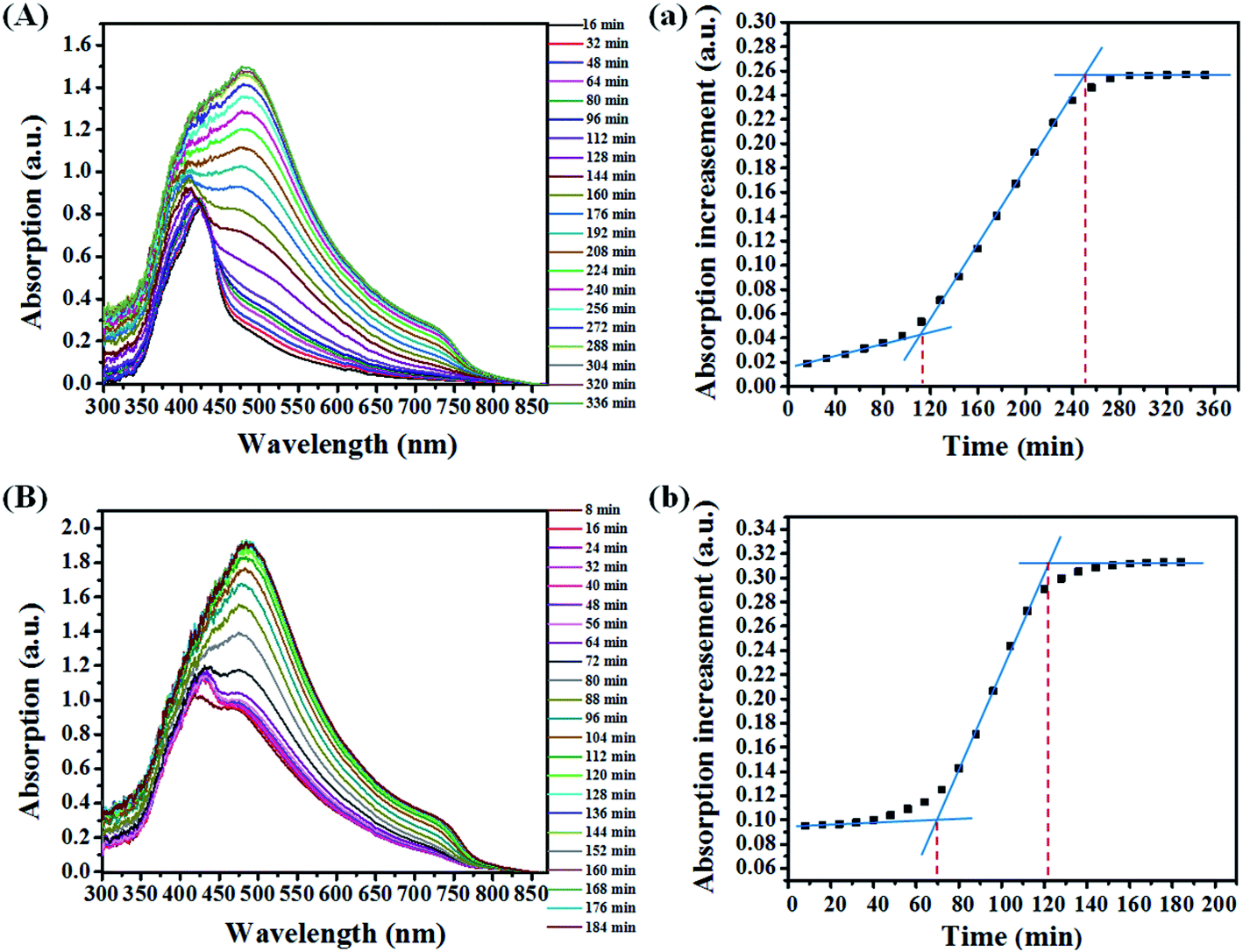 | ||
| Fig. 3 The situ UV-vis absorption spectra of the perovskite film without (A) and with (B) SSA treatment; the evolution of absorption intensity at 730 nm of the perovskite film without (a) and with (b) SSA treatment. All the films to be thermally annealed were heated at 75 °C under flowing nitrogen. | ||
The optimized crystal orientation resulting from crystal growth kinetics
In order to get further insight into the crystal structure, out of plane X-ray diffraction (XRD) was performed. As shown in Fig. 4, two obvious peaks are found at 14.08° and 28.5°, which can be assigned to the (110) and (220) crystal planes of the hybrid perovskite orthorhombic lattice. While for the treated film, except the (h k 0) (h = k) diffraction signals, the peaks located at 31.9°, 40.7°, and 43.3° corresponding to (310), (224) and (314) diffraction signals are also obvious. The appearance of these diffraction signals indicated that the orientation of perovskite crystals must be changed after the SSA treatment.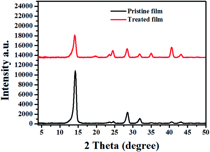 | ||
| Fig. 4 The out of plane XRD profile shows the crystallinity of the pristine and treated perovskite film. | ||
In order to probe the orientations of perovskite crystals, two-dimensional GIXD (2D-GIXD) was performed. As shown in Fig. 5A, the 2D-GIXD result obtained for the pristine film exhibits a concentrated “spotty” pattern along the qz axis at azimuthal angle 90° (the scattering signals at q = 10 nm−1 are assigned to the (110) plane of the perovskite structure28), signifying that (h k 0) (h = k) signals are highly oriented in the out-of-plane direction (the schematic diagram is shown in Fig. 5E). Nevertheless, the spotty pattern of the treated film splits into several points and their azimuthal angles are distributed at 22.5°, 45°, 66.5° and 90°, respectively. According to the dihedral angle relationship (shown in S5), when the (h k 0) (h = k) signal is centered at 45°, its (h 0 0) lattice planes must be perpendicular to the substrate as shown in Fig. 5F. To quantify the amount of crystals that adopt different orientations, we calculated the two-dimensional signal intensity according to the azimuthal angle (Fig. 5C corresponds to Fig. 5A and Fig. 5D corresponds to Fig. 5B). The area under the azimuthal curve is in proportion to the crystallinity of the perovskite film. As a result, we could compare the number of crystals that adopted different orientations. Here, the whole relative crystallinity degree of the pristine film is 49259 (A10–90 = 49259) and that of the treated film is 59269 (A20–90 = 59269), which implies the enhanced crystallinity of perovskite after the SSA treatment. Furthermore, the ratio of crystals that adopted (h 0 0) orientation (A135–55/A10–90) for the pristine film is 12.7%, while the corresponding ratio (A235–55/A20–90) increased to 26.3% after the SSA treatment. These changes suggest that the SSA treatment promoted the crystals to adopt (h 0 0) orientation. According to the perovskite crystal structure, the crystals adopted the (h 0 0) orientation, i.e. the corner of the inorganic framework would make contact between the perovskite and substrate interface, which may be beneficial for carrier transportation and collection due to higher carrier mobility.29,30 As far as we know, this is the first time to adjust the orientation of perovskite, which is meaningful to understand the fundamental crystal structure.
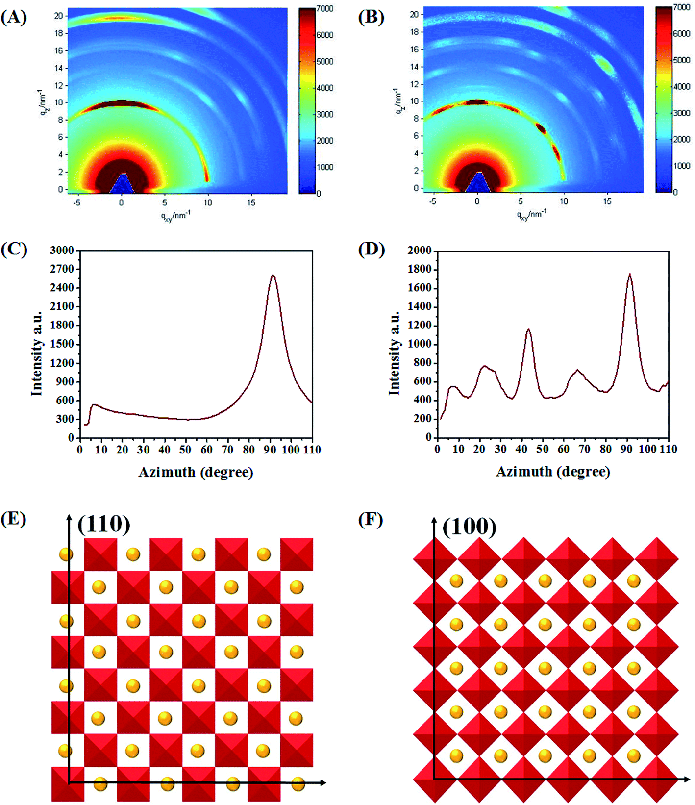 | ||
| Fig. 5 The 2D-GIXD patterns of pristine (A) and treated (B) perovskite films. Azimuthal line scans for the (110) peak of the pristine (C) and treated (D) perovskite films. The schematic diagram of the crystals adopted (h k 0) (h = k) orientation (E) and (h 0 0) orientation (F). | ||
To probe the evolution of perovskite orientation, we employed In situ smart with 2D detection capability (In situ 2D-GIXD). As shown in Fig. 6A, three diffraction signals for the pristine film were observed before thermal annealing. Combining the 2D-smart with Rigaku 2D Data Processing software, these three signals are assigned to 11.0°, 12.2° and 16.5° (Fig. S6†), which are the diffraction signals of lead halide.22,27 After thermal annealing, the signal intensity of lead halide became weak, while the signal corresponding to CH3NH3PbI3−xClx (14.2°) appeared (84 min) and its intensity became stronger gradually (84–224 min). It implies the film underwent a complete transition from lead halide to perovskite. Moreover, the signal of perovskite is also distributed along the qz axis, which suggests that the (h k 0) (h = k) crystal plane is highly oriented in the out-of-plane direction. However, the transition process for the treated film is different as shown in Fig. 6B. At the beginning, not only the lead halide signal but also the perovskite signal could be observed. Moreover, the signal of lead halide was weak while the signal of perovskite was relatively strong, and all of them were distributed around the qz axis. Both of these demonstrate that the SSA treatment could promote the formation of the perovskite nucleus, which is consistent with the XRD as shown in Fig. S2.† During the thermal annealing process, lead halide transformed into perovskites gradually. Surprisingly, in addition to the azimuth angle of 90°, the signal of perovskite also appeared around an azimuth angle of 45° (42 min) and its intensity became stronger. This phenomenon indicates that some of the formed perovskite rearranged and adopted (h 0 0) orientation during the thermal annealing process. This dynamic change about the crystal orientation of perovskite is a novel observation and may be useful to understand the perovskite formation dynamics.
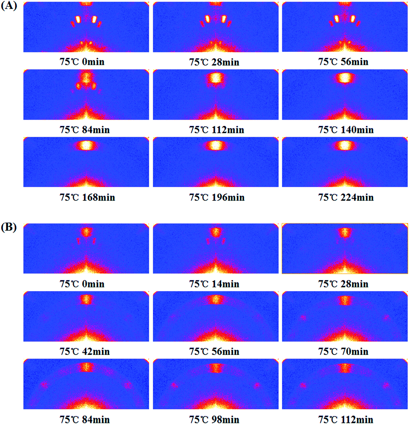 | ||
| Fig. 6 The In situ 2D-GIXD patterns for the pristine (A) and treated (B) perovskite film. All the films to be thermally annealed were heated at 75 °C. | ||
From the above results, the mechanism of optimizing film morphology and orientation via SSA treatment can be concluded as follows (as shown in Scheme 1): during the SSA process, IPA promotes the precipitation and crystallization of lead halide (as shown in Fig. S8†) because it has a low solubility to lead halide. Furthermore, IPA assists the diffusion of MA+ and I− since it acts as a good solvent for MAI and forms H-bonding with MA+, thus promoting the intercalation of MA+ into an inorganic framework, resulting in the formation of a uniform perovskite crystal nucleus. During the thermal annealing process, the nucleus would rearrange and coalesce via the Ostwald ripening process to attain thermodynamic stability owing to the surface energy minimization, which results in an increased crystal growth rate and optimized crystal orientation.
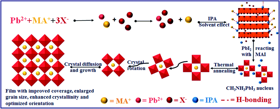 | ||
| Scheme 1 The schematic diagram of the nucleation process during the SSA process and crystal growth during the thermal annealing process. | ||
Enhanced photoabsorption and carrier extraction efficiency
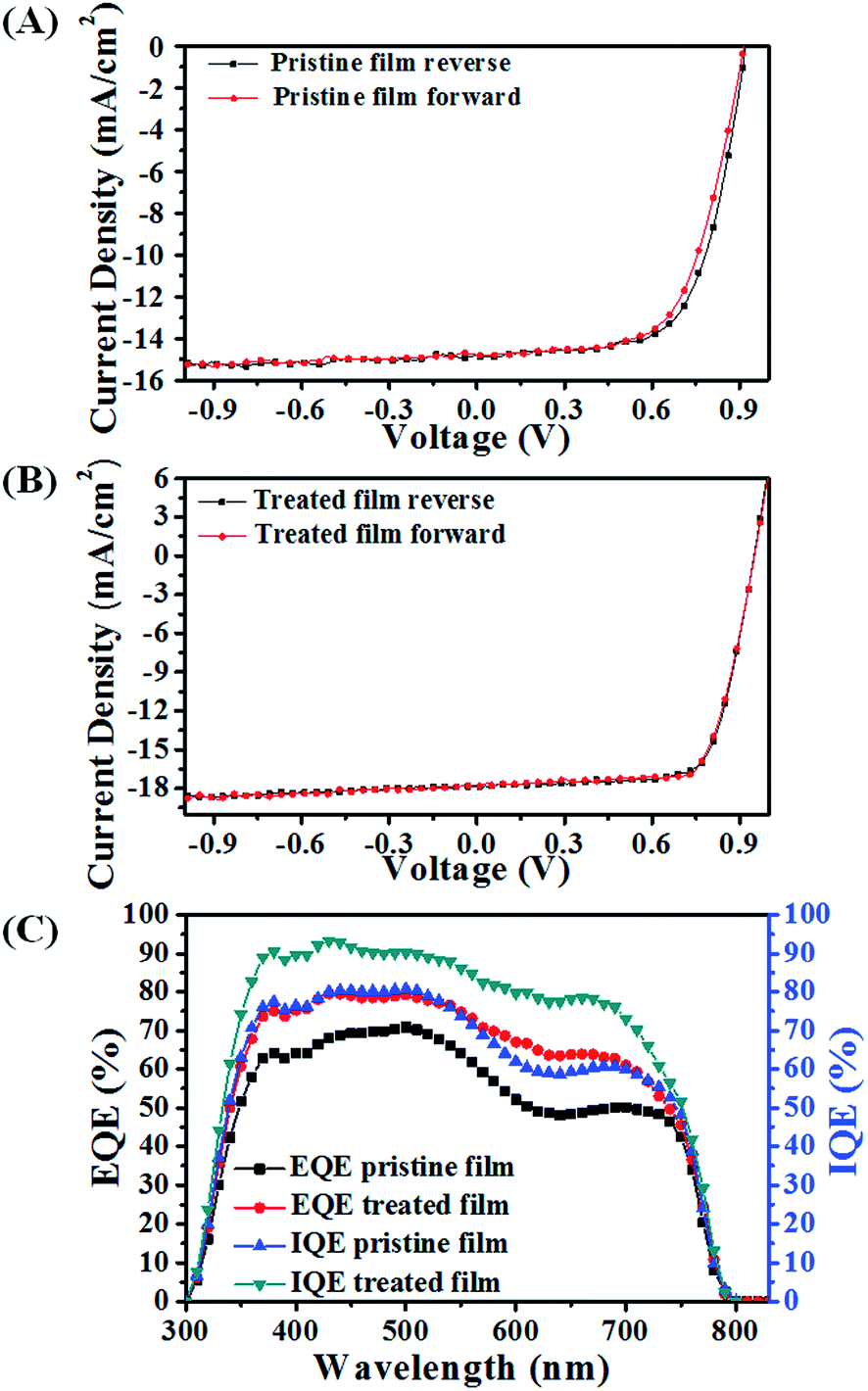
As is well known, the morphology of the perovskite film has profound influence on device performance. Here, we improved the crystallinity and coverage as well as orientation of the perovskite film, which resulted in an increased light harvesting, longer carrier lifetime and higher carrier extraction efficiency.The device parameters for the pristine film and treated film were extracted from the reverse and forward current–voltage (J–V) curves under simulated AM1.5, 100 mW cm−2 sunlight (as shown in Fig. 7).31 The device based on the pristine perovskite film exhibits a reverse short-circuit current density (JSC), an open-circuit voltage (VOC) and a fill factor (FF) of 14.83 mA cm−2, 0.91 V and 0.67, respectively, with a low power conversion efficiency (PCE) of 9.04%. While the performance of the device based on the treated film increased to 12.38%, with an improved reverse JSC, VOC and FF of 17.85 mA cm−2, 0.95 V, and 0.73, respectively. The forward J–V curves of the device with and without SSA treatment were also obtained, and its corresponding parameters are listed in Table 1. There is no big discrepancy between the reverse and forward device parameters, indicating the reliability of J–V curve measurement. After SSA treatment, the higher VOC could be ascribed to the well-developed crystals and optimized crystal orientation, which reduce the energy losses during the carrier transport process. The increase of JSC is mainly attributed to the enhanced absorption, arising from the enhanced crystallinity and increased film coverage. In addition, the increased JSC is in good agreement with external quantum efficiency (EQE) measurement (Fig. 7B), which has an error range of 2%. Moreover, the device with SSA treatment also shows a higher FF, which implies a reduced recombination during the charge transport process.
 | ||
| Fig. 7 The J–V curve for the devices based on the pristine (A) and treated (B) perovskite film, the forward (short circuit → open circuit) and reverse (open circuit → short circuit) scans with 10 mV voltage steps under 100 mW cm−2 simulated AM1.5G illumination. (C) The EQE and IQE plot of devices based on the pristine and treated perovskite film. | ||
| V OC (V) | J SC (mA cm−2) | FF | PCE (%) | |
|---|---|---|---|---|
| Pristine film reverse | 0.92 | 14.68 | 0.67 | 9.04 |
| Pristine film forward | 0.91 | 14.81 | 0.66 | 8.89 |
| Treated film reverse | 0.95 | 17.85 | 0.73 | 12.38 |
| Treated film forward | 0.95 | 17.84 | 0.73 | 12.37 |
In order to confirm our viewpoint, the internal quantum efficiency (IQE) is calculated. Assuming that all of the light transmitted through ITO/glass was absorbed by the perovskite film, the IQE was calculated by dividing the EQE by the transmittance (Fig. S12†).24,31 The device fabricated by the treated film exhibits a higher IQE over the whole spectrum, which indicates that the photogenerated carriers are collected at the electrodes with few losses. The increased IQE must be caused by the enhanced crystallinity, grain size and optimization of crystal orientation. Due to a higher crystallinity and large crystals, the number of defects and grain boundaries is reduced, leading to fewer trapped free carriers.8 Moreover, the optimized orientation with an inorganic framework perpendicular to the substrate would further decrease the barrier energy of charge transport, which is beneficial to the charge extraction.
The reduced recombination of carriers was also reflected by its prolonged lifetime. Fig. 8 shows the femtosecond transient absorption (fs-TA) spectra on the pristine film and treated film. In our experiment, the decay kinetics of the TA signal for the perovskite films monitored at a wavelength of 750 nm, extracted from the perovskite films prepared on the glass substrate. As we can see, there are two photobleaching (PB) negative peaks around 475 nm and 750 nm and the photoabsorption (PA) peak at 500–700 nm, which is consistent with previous reports.32 The fs-TA spectra of the treated film show stronger PB intensity, which means the number of photogenerated carriers is much bigger than the one in the pristine film. This is also in line with the enhanced photoabsorption as shown in the UV-vis absorption spectrum, indicating an intense absorption of the perovskite excited states due to the enhanced crystallinity. To illustrate the charge recombination and transport properties, the decay kinetics of the TA signal for the pristine film and treated film were employed (Fig. 8C). Asufit fits were performed to quantify the carrier kinetics. According to Asufit, the curve obtained from the pristine film is fitted with two time constants, the fast component (39 ps) and slow component (180 ps). According to previous reports,33–35 the fast decay component might result from grain boundaries within the perovskite film, which could trap charge carriers. The long decay component could be attributed to the recombination of free carriers in the radiative channel. After the SSA, the sample only exhibited a slow decay component. The absence of the fast decay component may be originated from enhanced crystallinity and enlarged crystal size, which reduced the number of grain boundaries, consequently, reducing the number of trapped charge carriers. Moreover, the slow decay component was prolonged to 335 ps, which is almost twice than the one in the pristine film. This prolonged slow decay component might result from the improved morphology, enhanced crystallization and optimized orientation, which retarded the recombination of free carriers, representing a longer carrier lifetime.
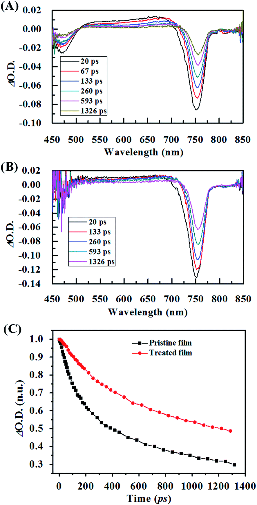 | ||
| Fig. 8 (A) Transient-absorption spectra at several delay times following excitation at 400 nm for pristine (A) and treated (B) perovskite films. (C) The transient decay dynamics of pristine and treated perovskite films; the pump wavelength is 750 nm. | ||
Conclusion
In summary, the nucleation kinetics and crystal growth of CH3NH3PbI3−xClx hybrid perovskite were regulated by the SSA method, producing a continuous film with enlarged grain size, enhanced crystallinity and optimized orientation. The improved film morphology is mainly attributed to the formation of the uniform perovskite nucleus and fast crystal growth caused by the SSA process. In the SSA process, IPA would promote the crystallization of lead halide and the intercalation of MAI due to the selective solubility, leading to the formation of the uniformly distributed perovskite nucleus. The formation of the nucleus avoids the slowness and inconformity of the nucleation process in traditional film fabrication and favors the crystal growth process, resulting in improved film coverage, enlarged grain size and enhanced crystallinity. Furthermore, the formed nucleus would rearrange via Ostwald ripening during the thermal annealing process, resulting in the crystal that adopts the (h 0 0) orientation to attain thermodynamic stability. The improved film coverage, enlarged crystal size, enhanced crystallinity and optimized crystal orientation are beneficial for the carrier collection due to the prolonged carrier life time and reduced carrier recombination, which resulted in an improvement of PCE from 9.04% to 12.38%, about 37% increase compared with that of the reference device.Acknowledgements
This work was supported by the National Basic Research Program of China (973 Program-2014CB643505), the Strategic Priority Research Program of the Chinese Academy of Science (Grant No. XDB12020300). We also thank the Shanghai Synchrotron Radiation Facility (SSRF) for 2D GIXD measurement.References
- L. Zuo, Z. Gu, T. Ye, W. Fu, G. Wu, H. Li and H. Chen, J. Am. Chem. Soc., 2015, 137, 2674–2679 CrossRef CAS PubMed.
- A. Kojima, K. Teshima, Y. Shirai and T. Miyasaka, J. Am. Chem. Soc., 2009, 131, 6050–6051 CrossRef CAS PubMed.
- H. Zhou, Q. Chen, G. Li, S. Luo, T.-B. Song, H.-S. Duan, Z. Hong, J. You, Y. Liu and Y. Yang, Science, 2014, 345, 542–546 CrossRef CAS PubMed.
- J.-W. Lee, T.-Y. Lee, P. J. Yoo, M. Gratzel, S. Mhaisalkar and N.-G. Park, J. Mater. Chem. A, 2014, 2, 9251–9259 CAS.
- W. S. Yang, J. H. Noh, N. J. Jeon, Y. C. Kim, S. Ryu, J. Seo and S. I. Seok, Science, 2015, 348, 1234–1237 CrossRef CAS PubMed.
- L. Wang, W. Fu, Z. Gu, C. Fan, X. Yang, H. Li and H. Chen, J. Mater. Chem. C, 2014, 2, 9087–9090 RSC.
- W. Nie, H. Tsai, R. Asadpour, J.-C. Blancon, A. J. Neukirch, G. Gupta, J. J. Crochet, M. Chhowalla, S. Tretiak, M. A. Alam, H.-L. Wang and A. D. Mohite, Science, 2015, 347, 522–525 CrossRef CAS PubMed.
- Q. Chen, H. Zhou, Z. Hong, S. Luo, H.-S. Duan, H.-H. Wang, Y. Liu, G. Li and Y. Yang, J. Am. Chem. Soc., 2014, 136, 622–625 CrossRef CAS PubMed.
- W. Zhang, M. Saliba, D. T. Moore, S. K. Pathak, M. T. Hörantner, T. Stergiopoulos, S. D. Stranks, G. E. Eperon, J. A. Alexander-Webber, A. Abate, A. Sadhanala, S. Yao, Y. Chen, R. H. Friend, L. A. Estroff, U. Wiesner and H. J. Snaith, Nat. Commun., 2015, 6, 6142–6151 CrossRef CAS PubMed.
- H. Wang, Y. He, Y. Li and H. Su, J. Phys. Chem. A, 2012, 116, 255–262 CrossRef CAS PubMed.
- Q. Dong, Y. Fang, Y. Shao, P. Mulligan, J. Qiu, L. Cao and J. Huang, Science, 2015, 347, 967–969 CrossRef CAS PubMed.
- D. Shi, V. Adinolfi, R. Comin, M. Yuan, E. Alarousu, A. Buin, Y. Chen, S. Hoogland, A. Rothenberger, K. Katsiev, Y. Losovyj, X. Zhang, P. A. Dowben, O. F. Mohammed, E. H. Sargent and O. M. Bakr, Science, 2015, 347, 519–522 CrossRef CAS PubMed.
- N. J. Jeon, J. H. Noh, Y. C. Kim, W. S. Yang, S. Ryu1 and S. I. Seok, Nat. Mater., 2014, 13, 897–903 CrossRef CAS PubMed.
- Y. Tidhar, E. Edri, H. Weissman, D. Zohar, G. Hodes, D. Cahen, B. Rybtchinski and S. Kirmayer, J. Am. Chem. Soc., 2014, 136, 13249–13256 CrossRef CAS PubMed.
- M. Saliba, K. W. Tan, H. Sai, D. T. Moore, T. Scott, W. Zhang, L. A. Estroff, U. Wiesner and H. J. Snaith, J. Phys. Chem. C, 2014, 118, 17171–17177 CAS.
- M. Xiao, F. Huang, W. Huang, Y. Dkhissi, Y. Zhu, J. Etheridge, A. Gray-Weale, U. Bach, Y.-B. Cheng and L. Spiccia, Angew. Chem., Int. Ed., 2014, 53, 1–7 CrossRef.
- S. T. Williams, F. Zuo, C.-C. Chueh, C.-Y. Liao, P.-W. Liang and A. K.-Y. Jen, ACS Nano, 2014, 8, 10640–10654 CrossRef CAS PubMed.
- M. I. Dar, N. Arora, P. Gao, S. Ahmad, M. Grätzel and M. K. Nazeeruddin, Nano Lett., 2014, 14, 6991–6996 CrossRef CAS PubMed.
- Y. Wu, A. Islam, X. Yang, C. Qin, J. Liu, K. Zhang, W. Penga and L. Han, Energy Environ. Sci., 2014, 7, 2934–2938 CAS.
- P.-W. Liang, C.-Y. Liao, C.-C. Chueh, F. Zuo, S. T. Williams, X.-K. Xin, J. Lin and A. K. Y. Jen, Adv. Mater., 2014, 26, 3748–3754 CrossRef CAS PubMed.
- Z. Xiao, Q. Dong, C. Bi, Y. Shao, Y. Yuan and J. Huang, Adv. Mater., 2014, 26, 6503–6509 CrossRef CAS PubMed.
- Y. Zhao and K. Zhu, J. Am. Chem. Soc., 2014, 136, 12241–12244 CrossRef CAS PubMed.
- E. Zimmermann, P. Ehrenreich, T. Pfadler, J. A. Dorman, J. Weickert and L. S-Mende, Nat. Photonics, 2014, 8, 669–672 CrossRef CAS.
- T. Vetter, M. Iggland, D. R. Ochsenbein, F. S. Hänseler and M. Mazzotti, Cryst. Growth Des., 2013, 13, 4890–4905 CAS.
- M. Xiao, F. Huang, W. Huang, Y. Dkhissi, Y. Zhu, J. Etheridge, A. Gray-Weale, U. Bach, Y.-B. Cheng and L. Spiccia, Angew. Chem., 2014, 126, 10056–10061 CrossRef.
- Y. Tidhar, E. Edri, H. Weissman, D. Zohar, G. Hodes, D. Cahen, B. Rybtchinski and S. Kirmayer, J. Am. Chem. Soc., 2014, 136, 13249–13256 CrossRef CAS PubMed.
- S. Ahmad, P. K. Kanaujia, W. Niu, J. J. Baumberg and G. Vijaya Prakash, ACS Appl. Mater. Interfaces, 2014, 6, 10238–10247 CAS.
- K. W. Tan, D. T. Moore, M. Saliba, H. Sai, L. A. Estroff, T. Hanrath, H. J. Snaith and U. Wiesner, ACS Nano, 2014, 8, 4730–4739 CrossRef CAS PubMed.
- P. Gao, M. Grätzel and M. K. Nazeeruddin, Energy Environ. Sci., 2014, 7, 2448–2463 CAS.
- A. Mei, X. Li, L. Liu, Z. Ku, T. Liu, Y. Rong, M. Xu, M. Hu, J. Chen, Y. Yang, M. Grätzel and H. Han, Science, 2014, 345, 295–298 CrossRef CAS PubMed.
- A. C. Jeffrey, S. M. Joseph and V. K. Prashant, J. Phys. Chem. Lett., 2015, 6, 852–857 CrossRef PubMed.
- J. Seo, S. Park, Y. C. Kim, N. J. Jeon, J. H. Noh, S. C. Yoon and S. I. Seok, Energy Environ. Sci., 2014, 7, 2642–2646 CAS.
- L. Wang, C. McCleese, A. Kovalsky, Y. Zhao and C. Burda, J. Am. Chem. Soc., 2014, 136, 12205–12208 CrossRef CAS PubMed.
- J. S. Manser and P. V. Kamat, Nat. Photonics, 2014, 8, 737–743 CrossRef CAS.
- C. S. Ponseca, T. J. Savenije, M. Abdellah, K. Zheng, A. Yartsev, T. Pascher, T. Harlang, P. Chabera, T. Pullerits, A. Stepanov, J.-P. Wolf and V. Sundström, J. Am. Chem. Soc., 2014, 136, 5189–5192 CrossRef CAS PubMed.
Footnote |
| † Electronic supplementary information (ESI) available. See DOI: 10.1039/c5ta08015k |
| This journal is © The Royal Society of Chemistry 2016 |