
 Open Access Article
 This Open Access Article is licensed under a Creative Commons Attribution-Non Commercial 3.0 Unported Licence
Two-in-one: cathode modification and improved solar cell blend stability through addition of modified fullerenes†
Zandra
George
a,
Yuxin
Xia
b,
Anirudh
Sharma
c,
Camilla
Lindqvist
d,
Gunther
Andersson
e,
Olle
Inganäs
b,
Ellen
Moons
d,
Christian
Müller
a and
Mats R.
Andersson
*ac
aDepartment of Chemistry and Chemical Engineering, Chalmers University of Technology, SE-412 96 Göteborg, Sweden
bBiomolecular and Organic Electronics, IFM and Center of Organic Electronics, Linköping University, SE-581 83 Linköping, Sweden
cFuture Industries Institute, University of South Australia, Mawson Lakes, South Australia 5095, Australia. E-mail: mats.andersson@unisa.edu.au
dDepartment of Engineering and Physics, Karlstad University, SE-65188 Karlstad, Sweden
eFlinders Centre for NanoScale Science and Technology, Flinders University, Sturt Road, Bedford Park, Adelaide, SA 5042, Australia
First published on 21st January 2016
Abstract
The synthesis of dual purpose modified fullerenes with pyridine- as well as amine-functional groups is reported. Addition of these fullerenes to a polymer![[thin space (1/6-em)]](https://www.rsc.org/images/entities/char_2009.gif) :fullerene bulk-heterojunction blend based on a thiophene–quinoxaline donor polymer is found to modify the active layer/cathode interface of inverted solar cells (glass/ITO/active layer/MoO3/Al). In particular the open-circuit voltage of devices is increased from 0.1 V to about 0.7 V, which results in a drastic rise in photovoltaic performance with a power conversion efficiency of up to 3%. At the same time, presence of the functionalised fullerene additives prevents the detrimental formation of micrometre-sized fullerene crystals upon annealing at 140 °C. As a result, the device performance is retained, which promises significantly increased thermal stability of the bulk-heterojunction blend nanostructure.
:fullerene bulk-heterojunction blend based on a thiophene–quinoxaline donor polymer is found to modify the active layer/cathode interface of inverted solar cells (glass/ITO/active layer/MoO3/Al). In particular the open-circuit voltage of devices is increased from 0.1 V to about 0.7 V, which results in a drastic rise in photovoltaic performance with a power conversion efficiency of up to 3%. At the same time, presence of the functionalised fullerene additives prevents the detrimental formation of micrometre-sized fullerene crystals upon annealing at 140 °C. As a result, the device performance is retained, which promises significantly increased thermal stability of the bulk-heterojunction blend nanostructure.
Introduction
Polymer solar cells have gained considerable interest during the last decades. The most promising active layer material comprises so-called bulk-heterojunction blends of a donor polymer that is finely mixed with a fullerene acceptor. The photovoltaic performance has increased rapidly over the last years with power conversion efficiencies now exceeding 10% for lab-scale single-junction devices.1 One advantage of polymer solar cells is the possibility to use roll-to-roll coating techniques for large-scale device production. However, several issues must be resolved before the efficiencies of lab-scale devices can be reproduced. Two critical aspects concern (1) the inverted geometry of large-area devices that typically require modification of the bottom electrode with interlayers, and (2) the thermal stability of the polymer:fullerene bulk-heterojunction nanostructure.
Inverted polymer solar cells have shown a superior stability compared to devices with conventional architecture.2,3 However, losses are often found due to limitations at the active layer/electrode interface, which can reduce the device performance. To improve the charge selectivity of the cathode, and thereby the overall performance of the device, significant research efforts have been dedicated towards modifying the work function of different electrode materials. The use of polymers or fullerene derivatives with functional groups such as tertiary amines as cathode interfacial materials has gained a lot of interest for both polymer solar cells and light emitting diodes. This approach permits to improve electron injection and extraction, energy level alignment and surface energy modification.4–9 Other types of interface layers have also been used to modify for example indium tin oxide (ITO) electrodes.10,11 Unfortunately, in our experience the interlayer materials that combine conjugated functionalities with amine derivatives give unstable modification of the electrode work function under ambient conditions, whereas stability is a prerequisite for a large scale roll-to-roll production process. Thus, it would be desirable to develop a method that permits to mitigate the limited stability of interlayer materials.
Rapid coating techniques must involve several heating steps for rapid solvent removal. Polyethylene terephthalate (PET) is the most widely considered substrate material, which can withstand processing temperatures of up to 140 °C.12 Therefore, it is crucial that the polymer:fullerene blend nanostructure offers good thermal stability. However, polymer:fullerene blends tend to coarsen when heated above the blend glass transition,13–15 which for the majority of studied materials lies below the required processing temperature.16 In addition, large micrometre-sized fullerene crystallites start to grow,17,18 which are detrimental for the device performance.15,19,20 One way to improve the thermal stability of polymer:fullerene blends is to use a fullerene mixture, which either hinders crystallisation of the fullerene acceptor,21–25 or results in a controlled nucleation of sub-micrometre-sized fullerene crystals.26,27
In this work we establish that fullerene mixtures can be used to simultaneously achieve both interlayer modification of the cathode and improved thermal stability of a polymer:fullerene bulk-heterojunction blend. Two easily synthesised fullerene derivatives (PCBA and PCBP; Fig. 1) were added to a polymer:fullerene blend comprising the thiophene–quinoxaline copolymer poly[2,3-bis-(3-octyloxyphenyl)quinoxaline-5,8-diyl-alt-thiophene-2,5-diyl] (TQ1; Fig. 1)28 and phenyl-C61-butyric acid methyl ester (PCBM; Fig. 1) to evaluate their performance in inverted solar cells (glass/ITO/active layer/MoO3/Al). The chemical structures of the two fullerene derivatives were designed in such a way that they modify the cathode interface and decrease the work function of ITO. The amine group on PCBA is similar to the one used on interlayer polymers previously published by us.29,30 This type of amine group has been shown to chemisorb to a number of different substrates, including ITO,31 and is therefore likely to induce a self-assembly of PCBA at the ITO-cathode. Importantly, it has recently been shown that a tertiary-amine functionalised fullerene self-assembles on the ITO-cathode of an organic solar cell when co-deposited in a binary or ternary mixture with the donor polymer poly(3-hexylthiophene).32,33 The nitrogen atom in the pyridine group on PCBP has similar chemical properties as the tertiary amine on PCBA and is therefore also expected to self-assemble at the ITO cathode, however pyridine functional groups have not been widely used to modify the cathode interface so far. This method of adding the interface modifier into the active solar cell material can potentially be used to avoid the exposure of the sensitive interface layer to the ambient environment and to facilitate large scale roll-to-roll-printing.
 | ||
| Fig. 1 Chemical structures of TQ1, PCBM, PCBA and PCBP. | ||
Experimental
Materials
PCBM (purity > 99%) was purchased from Solenne BV. TQ1 was prepared according to previously published procedures.28 TQ1 had a number-average molecular weight of ∼35 kg mol−1 (polydispersity index ∼ 2.5) determined with size exclusion chromatography relative to polystyrene standards.Synthetic procedure for PCBA and PCBP
:methanol (9:1) mixture as eluent. Thereafter the solvent amount was reduced, the product precipitated using methanol and finally phenyl-C61-butyric acid 2-dimethylaminoethyl ester was collected by filtration and dried to yield 0.17 g (16%).
UPS-measurements
Ultraviolet photoelectron spectroscopy (UPS) measurements were performed in an ultra-high vacuum (UHV) apparatus built by SPECS (Berlin, Germany) using a low intensity UV light (He I line). The base pressure of the UHV chamber is in the order of 10−10 mbar. The spectra of the electrons emitted from the samples were recorded at a pass energy of 10 eV, with a hemispherical Phoibos 100 energy analyser from SPECS. At this pass energy, the analyser has an energy resolution of 400 meV as evaluated from the Fermi edge of polycrystalline silver. The angle between the He*/UV light irradiation and the analyser is 54°. The UP spectra were acquired by applying a bias of 10 V to the sample to clearly observe the secondary electron cut-off. The work function of the samples was determined from the secondary electron cut-off of the UP spectra.ITO was cleaned by standing in detergent solution for 20 min, followed by dump rinsing in DI water. Substrates were then successively sonicated in DI water, acetone and isopropanol for 10 minutes each. After blow drying the substrates with nitrogen, ITO substrates were then cleaned using TL-1 treatment (a mixture of water, ammonia (25%), and hydrogen peroxide (28%); 5:1:1 by volume). The ITO sample was transferred to the load lock for UPS measurement. Remaining cleaned ITO substrates were transferred to the glovebox for spin coating of PCBA, PCBP and PCBM at 5000 rpm for 60 s (2 mg ml−1 in o-DCB). Prepared samples were immediately transferred to the load lock for UPS measurements, with an exposure of less than two minutes to the ambient atmosphere.
Contact angle measurements
Static contact angle of de-ionized water against the surfaces was measured using a PAT-1 tensiometer supplied by Sinterface Technologies (Berlin, Germany). The ITO was cleaned as described for the UPS-measurements. The reported contact angles are average values measured over a period of 60 seconds keeping the volume of the droplet constant. The BHJ layer was washed by spin coating pure o-DCB over BHJ coated substrates at 3000 rpm for 60 s.Thin film preparation for optical microscopy, AFM and SEM
Thin films were spin-coated from either from o-DCB solutions (25 g L−1), where the concentration indicates the total material content in the solution. Solutions were heated to ∼60 °C prior to spin-coating. ITO-substrates were ultra-sonicated in acetone and iso-propanol respectively and blow dried with synthetic air prior to spin-coating. Annealing of films was done on a heating plate calibrated with K-type self-adhesive thermocouples from Omega (estimated error ±5 °C; time to reach stable temperature ∼30 s).Optical microscopy
Micrographs were recorded with a Zeiss Axio Scope A1 in reflection mode before and after annealing.Atomic force microscopy (AFM)
Measurements were done with a Digital Instrument Nanoscope IIIa equipped with a type G scanner (Digital Instrument Inc., Santa Barbara, USA). The measurements were done in tapping mode and in air using a Micro Masch NSC 15 silicon cantilever.Scanning electron microscopy (SEM)
Measurements were done with a Leo Ultra 55 SEM equipped with a field emission gun (LEO Electron Microscopy Group, Germany) and a secondary electron detector. The acceleration voltage was 3 kV.Photoluminescence quenching
An Oriel optical light guide was located as close to the biased cell as possible and connected to the entrance slit of the spectrometer. A Newton electron-multiplying CCD (charge-coupled device) Si array detector cooled to −60 °C in conjunction with a Shamrock sr 303i spectrograph from Andor Technology served as the emission–detection system. The system was wavelength-calibrated by an argon lamp to a resolution better than 0.5 nm. The transmission of the entire fibre-monochromator–CDD system was further radiometrically calibrated by an Optronic OL245M standard spectral irradiance lamp. The CCD detector is ‘back illuminated’, which increases the sensitivity but unfortunately also gives rise to some interference effects at wavelengths between 850 and 1000 nm. The pumping light is 405 nm blue laser.Differential scanning calorimetry (DSC)
Measurements were performed under nitrogen at a scan rate of 10 °C min−1 with a Mettler DSC2 calorimeter equipped with a HSS7 sensor and a TC-125MT intracooler. Samples were prepared by collecting drop-casted films of 1:1 TQ1:PCBM, 1:0.8:0.2 TQ1:PCBM:PCBA and 1:0.8:0.2 TQ1:PCBM:PCBP respectively in aluminium pans.
Device fabrication
Solar cells were fabricated using inverted structure; glass/ITO/active layer (90 nm)/MoO3 (9.5 nm)/Al (90 nm). The ITO glass was cleaned with detergent and TL-1, as described for the UPS-measurements. The cleaned ITO glass was transferred into a glove box filled with N2, where the active layer was deposited. The active layers were spin-coasted from o-DCB solutions resulting in a thickness of ∼90 nm. Some of the active layers were annealed for 15 min at 140 °C. After annealing, MoO3 and Al were deposited by thermal evaporation under a pressure less than 1 × 10⁻⁵ mbar. The active area of the solar cells was ∼0.046 cm2. The J–V data were measured using a Keithley 2400 Source Meter under AM 1.5G illumination from solar simulator (Model SS-50A, Photo Emission Tech., Inc.) with an intensity of 100 mW cm−2. The thickness of the active layers was determined using a Dektak surface profiler.Results and discussion
Material synthesis
In our design, the two different nitrogen-containing compounds were selected to investigate if there is a difference in using tertiary amines or pyridines as interface materials (Fig. 1). PCBA and PCBP were easily synthesised starting from PCBM through a transesterification reaction with 2-dimethylaminoethanol (for PCBA) or 4-(4′-pyridinyl)-butan-1-ol (for PCBP) using dibutyltin oxide as a catalyst.34 The reaction was monitored by matrix-assisted laser desorption/ionisation time-of-flight (MALDI-TOF) until completion, resulting in PCBA (16% yield) and PCBP (88% yield). The yield for PCBA was significantly lower due to large amounts of side reactions occurring during the synthesis.Work function modification
To study the influence of fullerenes on the ITO surface work function, UPS measurements were performed. Fig. 2 shows the UP spectra of clean ITO and ITO modified using PCBA and PCBP. The work function of ITO was found to be 5.0 ± 0.1 eV whereas both PCBA and PCBP modification of ITO surface was found to significantly reduce the electrode work function to 3.8 ± 0.1 eV and 4.0 ± 0.1 eV, respectively. Interestingly the reduction of the work function is similar for the tertiary-amine and the pyridine functionalised fullerenes indicating that pyridine compounds can also be used to modify the surface work function. So far in the literature mainly aliphatic amino compounds have been used. For comparison, a PCBM modified surface prepared in the same way was found to have a work function of 4.6 ± 0.1 eV.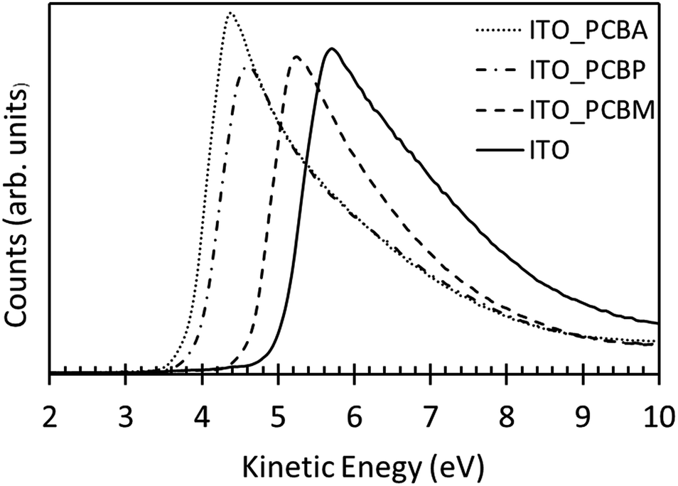 | ||
| Fig. 2 UP spectra of cleaned ITO and ITO surface modified with PCBA, PCBP and PCBM. | ||
Surface energy
We anticipate that during deposition of the active layer, the amine-functionalised fullerene derivative tends to self-assemble at the interface of the ITO cathode.30 This self-organisation is driven by chemisorption of the nitrogen functional groups onto the ITO and the molecules modify the surface energy of the ITO electrode. We inferred the change in substrate surface energy due to absorption of the amine-functionalised fullerene by measuring the water contact angle on ITO-substrates. First, thin films of TQ1:PCBM:PCBA and TQ1:PCBM:PCBP ternary blends as well as reference TQ1:PCBM were spin-coated from o-DCB solutions onto ITO substrates. Then, samples were rinsed with o-DCB to remove (the majority of) non-chemisorbed material, thus uncovering the PCBA or PCBP modified ITO substrate. Cleaned ITO showed a contact angle of ∼20° and after treatment with o-DCB 58°. ITO substrates that were initially coated with reference TQ1:PCBM or ternary blends displayed a contact angle of ∼95°, indicating that the top surface has a similar composition for all these blends (Table 1). After washing with o-DCB a clear difference can be seen in the contact angle for these surfaces indicating a change in surface energy that we rationalise with the chemisorption of PCBA and PCBP onto the ITO. Note that we cannot rule out the presence of residual PCBM and/or TQ1 on the washed surfaces. This indicates that a layer of nitrogen-functionalised fullerenes is present at the ITO surface in the ternary blends.
| Contact angle (°) | Contact angle after washing with o-DCB (°) | |
|---|---|---|
| a PCBM, PCBA and PCBP were spin coated (2 mg ml−1 in o-DCB) at 5000 rpm for 60 s. b PCBM was spin coated (20 mg ml−1 in chloroform) at 2000 rpm for 60 s. | ||
| ITO | ∼20 | 58 |
| ITO/PCBMa | ∼35 | — |
| ITO/PCBMb | 86 | — |
| ITO/PCBAa | 75 | — |
| ITO/PCBPa | 75 | — |
| ITO/TQ1:PCBM 1:1 |
95 | 50 |
| ITO/TQ1:PCBM:PCBA 1:0.8:0.2 |
94 | 88 |
| ITO/TQ1:PCBM:PCBP 1:0.8:0.2 |
96 | 84 |
Thermal stability
Optical microscopy was used to examine the effect of PCBA and PCBP on the crystallisation of PCBM in the TQ1:fullerene blend. The glass transition temperature of the TQ1:PCBM blend has previously been determined to be ∼110 °C.15,18 Thin films of ref. 1:1 TQ1:PCBM as well as 1:0.9:0.1 TQ1:PCBM:PCBA and 1:0.9:0.1 TQ1:PCBM:PCBP ternary blends were spin-coated from o-DCB solutions and annealed at 140 °C for 15 min. Optical microscopy of neat TQ1:PCBM films reveals distinct, micrometre-sized fullerene crystals after annealing (Fig. 3b). In contrast, no visible crystals could be observed in case of films containing PCBA or PCBP (Fig. 3c and d). Likewise, scanning electron microscopy (SEM) of annealed films also feature micrometre-sized PCBM crystals and in addition reveal a coarser nanostructure for neat TQ1:PCBM compared to e.g. TQ1:PCBM:PCBA (Fig. 4). Coarsening of the TQ1:PCBM nanostructure after annealing is also seen by atomic force microscopy (AFM), as evidenced by an increase in surface roughness, Rrms from 0.5 nm to 1.8 nm (S1, ESI†). Instead, annealed ternary blend films continue to display a low Rrms of 0.5–0.6 nm. The difference in nanostructure is also confirmed by photoluminescence (PL) spectroscopy where neat TQ1:PCBM shows a much higher PL intensity after annealing compared to the films that contain PCBA or PCBP (Fig. S2, ESI†), indicating in case of the former a less finely intermixed blend with less contact between the donor polymer and fullerene molecules.
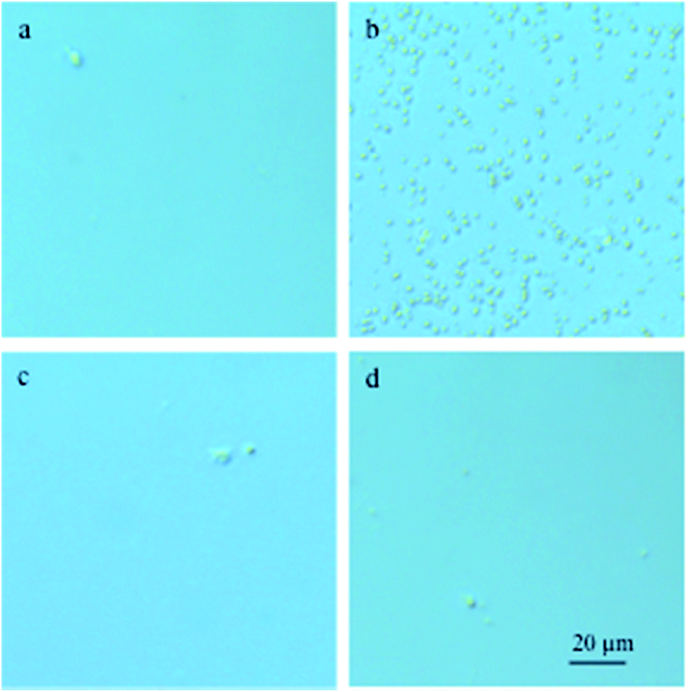 | ||
| Fig. 3 Optical micrographs of (a) un-annealed spin-coated 1:1 TQ1:PCBM, as well as films annealed at 140 °C for 15 min; (b) 1:1 TQ1:PCBM, (c) 1:0.9:0.1 TQ1:PCBM:PCBA, and (d) 1:0.9:0.1 TQ1:PCBM:PCBP. | ||
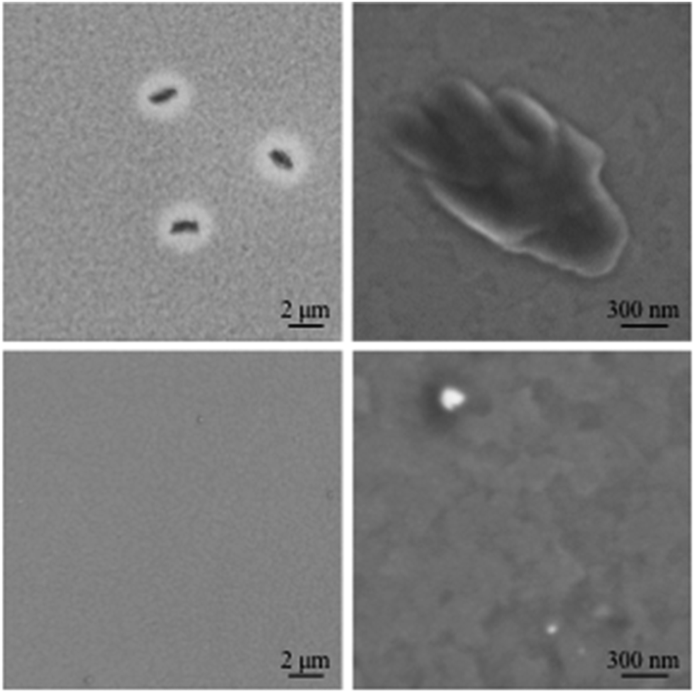 | ||
| Fig. 4 SEM micrographs of 1:1 TQ1:PCBM (top) and 1:0.8:0.2 TQ1:PCBM:PCBA (bottom) films annealed for 10 min at 140 °C. | ||
The thermal behaviour was further investigated using thermogravimetric analysis (TGA) and differential scanning calorimetry (DSC). The TGA measurements (Fig. S3, ESI†) reveal a limited thermal stability of the modified fullerene compounds with 5% weight loss at 242 °C and 307 °C for PCBA and PCBP, respectively. Thus, at the temperatures relevant for the annealing experiments no significant degradation is likely to occur. Second DSC heating and cooling thermograms (not shown) of solution-cast neat TQ1:PCBM feature a distinct endotherm with a peak at 272 °C and exotherm at 245 °C, respectively. In contrast, for ternary blends containing 10 wt% PCBP or PCBA no transitions could be discerned. Whilst some degradation of the modified fullerene compounds cannot be ruled out, exposure to unnecessarily high temperatures during DSC measurements was avoided by only heating to 285 °C, which lies just above the end-melting temperature of PCBM in neat TQ1:PCBM. Based on the performed DSC experiments we propose that the presence of PCBP and PCBA throughout the active material inhibits crystallisation of PCBM, which is in agreement with the absence of fullerene crystallites in spin-coated films as indicated by the recorded SEM and AFM images.
We would like to point out that changes in surface energy of the substrate can strongly affect the phase separation dynamics in polymer:fullerene thin films.35,36 Thus, it is feasible that besides interactions between PCBM and the amine-functionalised fullerene in the bulk of the film the self-assembled interlayer of PCBA or PCBP at the ITO cathode influences nanostructure formation in the here investigated ternary blends.
Photovoltaic devices
Finally, the photovoltaic performance of the two ternary blends as well as reference TQ1:PCBM solar cells was investigated before and after annealing (140 °C for 15 min) of the active layer (Table 2, Fig. 5) to further evaluate the effect of the modified fullerenes. To simplify the evaluation the polymer:fullerene ratio was kept constant at a 1:1 weight ratio. Standard devices of TQ1:PCBM using the same weight ratio have shown an efficiency of 3.5% in un-annealed devices.27 Inverted devices with an architecture of glass/ITO/active layer/MoO3/Al were prepared in N2 atmosphere by spin-coating o-DCB solutions on top of ITO. After spin-coating of the active layer, some of the samples were annealed in the dark, followed by evaporation of the anode materials. Devices with neat TQ1:PCBM show a very low VOC of 0.1–0.4 V, resulting in a low overall photovoltaic performance of 0.2%. Devices with a TQ1:PCBM:PCBA and TQ1:PCBM:PCBP active layer, however, display a VOC of 0.7–0.8 V and a power conversion efficiency (PCE) of 1–3%. The improvement in performance clearly indicates that both PCBA and PCBP alter the work function of ITO resulting in a better matching of the electrode energy levels to the active material, in agreement with the UPS measurements.
| Active layer blend | Annealing | J SC (mA cm−2) | V OC (V) | FF | PCE (%) (max. value) |
|---|---|---|---|---|---|
| TQ1:PCBM 1:1 |
— | 7.5 ± 0.3 | 0.10 ± 0.03 | 0.25 ± 0.05 | 0.2 ± 0.1 (0.3) |
| 140 °C, 15 min | 0.8 | 0.4 | 0.2 | 0.06 | |
| TQ1:PCBM:PCBA 1:0.9:0.1 |
— | 8.8 ± 0.3 | 0.73 ± 0.05 | 0.46 ± 0.05 | 2.9 ± 0.4 (3.3) |
| 140 °C, 15 min | 6.7 ± 0.7 | 0.65 ± 0.10 | 0.49 ± 0.01 | 2.1 ± 0.5 (2.6) | |
| TQ1:PCBM:PCBA 1:0.8:0.2 |
— | 6.5 ± 1.0 | 0.71 ± 0.05 | 0.36 ± 0.09 | 1.9 ± 0.3 (2.2) |
| 140 °C, 15 min | 4.9 ± 2.5 | 0.78 ± 0.10 | 0.48 ± 0.04 | 1.7 ± 0.5 (2.4) | |
| TQ1:PCBM:PCBP 1:0.9:0.1 |
— | 6.6 ± 1.4 | 0.76 ± 0.08 | 0.38 ± 0.10 | 1.9 ± 0.6 (2.5) |
| 140 °C, 15 min | 5.2 ± 0.8 | 0.69 ± 0.09 | 0.51 ± 0.01 | 1.8 ± 0.3 (2.1) | |
| TQ1:PCBM:PCBP 1:0.8:0.2 |
— | 4.8 ± 0.5 | 0.69 ± 0.05 | 0.31 ± 0.05 | 1.1 ± 0.2 (1.3) |
| 140 °C, 15 min | 3.8 ± 1.2 | 0.75 ± 0.07 | 0.49 ± 0.02 | 1.3 ± 0.3 (1.6) |
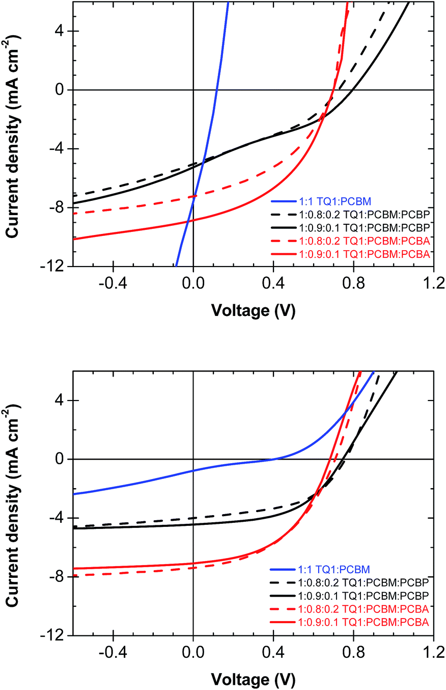 | ||
| Fig. 5 Representative IV-curves of photovoltaic devices before (top) and after annealing at 140 °C for 15 min (bottom). | ||
Annealing of TQ1:PCBM films at 140 °C resulted in a severe drop in short-circuit current density, JSC from initially 7.5 mA cm−2 to less than 1 mA cm−2 (Fig. 5), which we ascribe to the decreased polymer:fullerene interfacial area due to the formation of large PCBM crystals and phase separation of the blend. In contrast, ternary blend active layers annealed in the same way yield devices that retain their initial photocurrent and a JSC of 4–7 mA cm−2. In addition, TQ1:PCBM:PCBA and TQ1:PCBM:PCBP active layers also show a higher FF after annealing. This is ascribed to an enhanced concentration of PCBA and PCBP at the cathode upon annealing, which results in a reduction of the undesired charge flow at the cathode interface and hence an improved FF.37 Overall, annealing at 140 °C diminishes the efficiency of the TQ1:PCBM reference devices whereas ternary blend devices remain stable or even improve their photovoltaic performance. These differences in device performance are ascribed to the detrimental coarsening of the nanostructure as well as the growth of large PCBM crystals in TQ1:PCBM films. In contrast, the nanostructure of ternary blend films is preserved and, in addition, the ability of PCBA and PCBP to function as a self-assembling interlayer material provides a more favourable contact to the ITO-electrode.
Conclusions
In conclusion, PCBA and PCBP can act as self-assembling interlayer materials onto ITO surfaces, thus improving the photovoltaic performance of the described inverted solar cells. Both of the new fullerene molecules modify the work function of the ITO surface proving that also pyridine containing molecules can be used as interface layers to reduce the work function. Moreover, the use of fullerene mixtures is a viable strategy to improve and retain the photovoltaic performance of polymer solar cell blends that otherwise rapidly deteriorates at elevated temperatures. In particular, fullerene crystallisation of ternary blends that contain PCBA or PCBP is hindered at annealing temperatures that are suitable for roll-to-roll processes. Hence, the growth of micrometre-sized fullerene crystals is prevented despite annealing above the glass transition temperature of the blend, which in turn significantly enhances the thermal stability of the blend nanostructure. These findings are especially important for the manufacturability and long-term stability of printed polymer solar cells.Acknowledgements
The authors gratefully acknowledge funding from the Swedish Energy Agency and the Swedish Research Council, the Knut and Alice Wallenberg Foundation through a Wallenberg scholar grant to OI, and the Chinese Scholarship Council (CSC). We also thank Anders Mårtensson for carrying out the AFM measurements, Amaia Diaz de Zerio Mendaza for help with DSC and Xun Pan for the TGA measurements. MRA further acknowledges the South Australian government for financial support.Notes and references
- Y. Liu, J. Zhao, Z. Li, C. Mu, W. Ma, H. Hu, K. Jiang, H. Lin, H. Ade and H. Yan, Nat. Commun., 2014, 5, 5293 CrossRef CAS PubMed.
- C.-P. Chen, Y.-D. Chen and S.-C. Chuang, Adv. Mater., 2011, 23, 3859 CAS.
- J. J. Jasieniak, J. Seifter, J. Jo, T. Mates and A. J. Heeger, Adv. Funct. Mater., 2012, 22, 2594 CrossRef CAS.
- F. Zhang, M. Ceder and O. Inganäs, Adv. Mater., 2007, 19, 1835 CrossRef CAS.
- J. Luo, H. Wu, C. He, A. Li, W. Yang and Y. Cao, Appl. Phys. Lett., 2009, 95, 043301 CrossRef.
- C. He, C. Zhong, H. Wu, R. Yang, W. Yang, F. Huang, G. C. Bazan and Y. Cao, J. Mater. Chem., 2010, 20, 2617 RSC.
- W. Zhang, Y. Wu, Q. Bao, F. Gao and J. Fang, Adv. Energy Mater., 2014, 4, 1400359 Search PubMed.
- C. Duan, C. Zhong, C. Liu, F. Huang and Y. Cao, Chem. Mater., 2012, 24, 1682 CrossRef CAS.
- Y. Zhou, C. Fuentes-Hernandez, J. Shim, J. Meyer, A. J. Giordano, H. Li, P. Winget, T. Papadopoulos, H. Cheun, J. Kim, M. Fenoll, A. Dindar, W. Haske, E. Najafabadi, T. M. Khan, H. Sojoudi, S. Barlow, S. Graham, J.-L. Brédas, S. R. Marder, A. Kahn and B. Kippelen, Science, 2012, 336, 327 CrossRef CAS PubMed.
- S. Khodabakhsh, B. M. Sanderso, J. Nelson and T. S. Jones, Adv. Funct. Mater., 2006, 16, 95 CrossRef CAS.
- A. Savva, F. Petraki, P. Elefteriou, L. Sygellou, M. Voigt, M. Giannouli, S. Kennou, J. Nelson, D. D. C. Bradley, C. J. Brabec and S. A. Choulis, Adv. Energy Mater., 2013, 3, 391 CrossRef CAS.
- M. Jørgensen, K. Norrman, S. A. Gevorgyan, T. Tromholt, B. Andreasen and F. C. Krebs, Adv. Mater., 2012, 24, 580 CrossRef PubMed.
- S. Bertho, G. Janssen, T. J. Cleij, B. Conings, W. Moons, A. Gadisa, J. D'Haen, E. Goovaerts, L. Lutsen, J. Manca and D. Vanderzande, Sol. Energy Mater. Sol. Cells, 2008, 92, 753 CrossRef CAS.
- C. Müller, J. Bergqvist, K. Vandewal, K. Tvingstedt, A. S. Anselmo, R. Magnusson, M. I. Alonso, E. Moons, H. Arwin, M. Campoy-Quiles and O. Inganäs, J. Mater. Chem., 2011, 21, 10676 RSC.
- J. Bergqvist, C. Lindqvist, O. Bäcke, Z. Ma, Z. Tang, W. Tress, S. Gustafsson, E. Wang, E. Olsson, M. R. Andersson, O. Inganäs and C. Müller, J. Mater. Chem. A, 2014, 2, 6146 CAS.
- C. Müller, Chem. Mater., 2015, 27, 2740 CrossRef.
- X. Yang, J. K. J. van Duren, R. A. J. Janssen, M. A. J. Michels and J. Loos, Macromolecules, 2004, 37, 2151 CrossRef CAS.
- C. Lindqvist, A. Sanz-Velasco, E. Wang, O. Bäcke, S. Gustafsson, E. Olsson, M. R. Andersson and C. Müller, J. Mater. Chem. A, 2013, 1, 7174 CAS.
- S. Bertho, I. Haeldermans, A. Swinnen, W. Moons, T. Martens, L. Lutsen, D. Vanderzande, J. Manca, A. Senes and A. Bonfiglio, Sol. Energy Mater. Sol. Cells, 2007, 91, 385 CrossRef CAS.
- B. Conings, S. Bertho, K. Vandewal, A. Senes, J. D'Haen, J. Manca and R. A. J. Janssen, Appl. Phys. Lett., 2010, 96, 163301 CrossRef.
- H.-W. Liu, D.-Y. Chang, W.-Y. Chiu, S.-P. Rwei and L. Wang, J. Mater. Chem., 2012, 22, 15586 RSC.
- C.-Y. Chen, C.-S. Tsao, Y.-C. Huang, H.-W. Liu, W.-Y. Chiu, C.-M. Chuang, U. S. Jeng, C.-J. Su, W.-R. Wu, W.-F. Su and L. Wang, Nanoscale, 2013, 5, 7629 RSC.
- Y. Santo, I. Jeon, K. Sheng Yeo, T. Nakagawa and Y. Matsuo, Appl. Phys. Lett., 2013, 103, 073306 CrossRef.
- C. Lindqvist, J. Bergqvist, O. Bäcke, S. Gustafsson, E. Wang, E. Olsson, O. Inganäs, M. R. Andersson and C. Müller, Appl. Phys. Lett., 2014, 104, 153301 CrossRef.
- B. C. Schroeder, Z. Li, M. A. Brady, G. C. Faria, R. S. Ashraf, C. J. Takacs, J. S. Cowart, D. T. Duong, K. H. Chiu, C.-H. Tan, J. T. Cabral, A. Salleo, M. L. Chabinyc, J. R. Durrant and I. McCulloch, Angew. Chem., Int. Ed., 2014, 53, 12870 CrossRef CAS PubMed.
- J. J. Richards, A. H. Rice, R. D. Nelson, F. S. Kim, S. A. Jenekhe, C. K. Luscombe and D. C. Pozzo, Adv. Funct. Mater., 2013, 23, 514 CrossRef CAS.
- C. Lindqvist, J. Bergqvist, C.-C. Feng, S. Gustafsson, O. Bäcke, N. D. Treat, C. Bounioux, P. Henriksson, R. Kroon, E. Wang, A. Sanz-Velasco, P. M. Kristiansen, N. Stingelin, E. Olsson, O. Inganäs, M. R. Andersson and C. Müller, Adv. Energy Mater., 2014, 4, 1301437 Search PubMed.
- E. Wang, L. Hou, Z. Wang, S. Hellström, F. Zhang, O. Inganäs and M. R. Andersson, Adv. Mater., 2010, 22, 5240 CrossRef CAS PubMed.
- Z. Tang, L. M. Andersson, Z. George, K. Vandewal, K. Tvingstedt, P. Heriksson, R. Kroon, M. R. Andersson and O. Inganäs, Adv. Mater., 2012, 24, 554 CrossRef CAS PubMed.
- Z. George, E. Voroshazi, C. Lindqvist, R. Kroon, W. Zhuang, E. Wang, P. Henriksson, A. Hadipour and M. R. Andersson, Sol. Energy Mater. Sol. Cells, 2015, 133, 99 CrossRef CAS.
- Z. Tang, W. Tress, Q. Bao, M. J. Jafari, J. Bergqvist, T. Ederth, M. R. Andersson and O. Inganäs, Adv. Energy Mater., 2014, 4, 1400643 Search PubMed.
- D. Ma, M. Lv, M. Lei, J. Zhu, H. Wang and X. Chen, ACS Nano, 2014, 8, 1601 CrossRef CAS PubMed.
- M. Lv, M. Lei, J. Zhu, T. Hirai and X. Chen, ACS Appl. Mater. Interfaces, 2014, 6, 5844 CAS.
- D. F. Kronholm, J. C. Hummelen and A. B. Sieval, US Pat., 7,825,161, 2010.
- X. Bulliard, S.-G. Ihn, S. Yun, Y. Kim, D. Choi, J.-Y. Choi, M. Kim, M. Sim, J.-H. Park, W. Choi and K. Cho, Adv. Funct. Mater., 2010, 20, 4381 CrossRef CAS.
- C. M. Björström, S. Nilsson, A. Bernasik, A. Budkowski, M. Andersson, K. O. Magnusson and E. Moons, Appl. Surf. Sci., 2007, 253, 3906 CrossRef.
- A. Guerrero, B. Dörling, T. Ripolles-Sanchis, M. Aghamohammadi, E. Barrena, M. Campoy-Quiles and G. Garcia-Belmonte, ACS Nano, 2013, 7, 4637 CrossRef CAS PubMed.
Footnote |
| † Electronic supplementary information (ESI) available: AFM, photoluminescence quenching and TGA. See DOI: 10.1039/c5ta06420a |
| This journal is © The Royal Society of Chemistry 2016 |