
Controlling luminescent silicon nanoparticle emission produced by nanosecond pulsed laser ablation: role of interface defect states and crystallinity phase
T. G. Ulusoy Ghobadi†
 ab,
A. Ghobadi†bc,
T. Okyayd,
K. Topalliab and
A. K. Okyay‡
*abc
ab,
A. Ghobadi†bc,
T. Okyayd,
K. Topalliab and
A. K. Okyay‡
*abc
aUNAM – National Nanotechnology Research Center, Bilkent University, 06800 Ankara, Turkey. E-mail: aokyay@stanfordalumni.org
bInstitute of Materials Science and Nanotechnology, Bilkent University, 06800 Ankara, Turkey
cDepartment of Electrical and Electronics Engineering, Bilkent University, 06800 Ankara, Turkey
dOkyayTech R&D Ltd, Cyberpark, Bilkent University, 06800 Ankara, Turkey
First published on 21st November 2016
Abstract
In this study, we provide a systematic study on the origin of green and blue emission from luminescent silicon nanoparticles (Si-NPs) synthesized in water using a nanosecond pulsed laser ablation methodology. Here we report a direct one-step process to make ultra-small Si-NPs (∼3 nm mean size) by utilizing spiral beam scanning. In each ablation cycle, this scanning scheme collects generated nanoparticles towards the center and ablates them in subsequent cycles. Therefore, the resultant Si-NPs can reach very small sizes in a short time with high uniformity in their size distribution. Further, we investigate the effect of laser fluence on the emission properties of the obtained nanoparticles. For this aim, two different values of 60 mJ cm−2 and 30 mJ cm−2 laser fluences are employed to achieve green and blue emitting Si-NPs, respectively. Our results show that the emission spectrum for both blue and green Si-NPs has two main peaks at 426 nm and 520 nm, but their relative intensity ratios are different for these two cases. The findings of this study suggest that the blue emission originates from oxide related surface defects at the Si/SiOx interface, while the green emission stems from grain boundaries existing at the NP surface. We found that these two types of disorders can be controlled by tuning the laser power.
1 Introduction
Silicon, as the core of semiconductor technology, has been extensively employed in a variety of applications spanning from energy and environmental sciences to biomedical and biotechnologies. However, its inherent indirect band gap properties have limited its use in photovoltaic and light emitting diode applications. When the dimensions of Si nanoparticles (NPs) become comparable or smaller than Bohr radius of a bulk exciton (∼4 nm for Si),1–4 they undergo a remarkable transition from indirect to direct band gap semiconductor.5 Under such conditions, band-to-band radiative recombination (rather than phonon-assisted indirect transitions) begins to dominate Si-NPs' luminescence properties. The efficient luminescence of ultra-small silicon nanoparticle (Si-NPs) (<∼4 nm exciton Bohr radius of Si) opened myriad of possibilities in application areas such as solid state lighting,6 full color displays,7,8 optical sensors9 and fluorescent tags for biological imaging.10Up to now, several chemical and physical methods have been developed for the Si-NPs synthesis, including solution phase synthesis by reducing silicon halides,11–14 electrochemical etching of a silicon wafer with a mixed solution of aqueous HF, H2O2 and methanol,15,16 RF plasma decomposition of silane precursors (SiH4),17,18 and CO2 laser pyrolysis of silane.19,20 Although, chemical methods offer high control on particle size and surface properties but they usually have more complicated synthesis routes and several chemical precursors and reducing agents are involved during these processes. Thus each method requires optimization of chemical products, reducing agents or many steps for well controlled NP size. In recent years, pulsed laser ablation in liquid gathered immense interest as an efficient and alternative technique since it offers several advantages which can be listed as follows: (1) no material restriction compared to other techniques (2) no requirement for chemical precursors or reactions (3) no toxic by-products. However, the main drawback of this method is the limited control on the resulting size of the nanoparticles and their size distribution (homogeneity). To tackle with this problem, colloidal Si nanoparticles production has been studied employing different laser types with different wavelengths and pulse durations.21,22 In some of these studies, nanosecond laser pulses have been utilized which results in the formation of wide size distribution of nanoparticles which stabilize in the form of clusters.23,24 Therefore, some post-treatments are necessary to avoid agglomeration and enlarging of nanoparticles.25 This issue is less destructive for femtosecond laser in which a better size control mechanism can be obtained by tuning the laser pulse energy. On the other hand, several studies have been conducted to understand the essence of Si-NPs emission.
Several mechanisms have been proposed to explain emission properties of NPs.26–28 The main ones are quantum confinement effects, oxide related defects and combination of these two phenomena. However, its origin is still controversial and it highly depends on NPs preparation route. In present work, we propose a facile and widely adopted way to synthesize highly uniform sub-5 nm nanoparticles by combining pulsed laser ablation technique with spiral shaped laser beam scanning. In this type of scanning, the particles are collected towards the center of the spiral as they are produced and therefore re-ablated continuously in every cycle. Consequently, highly uniform ultra-small nanoparticles (with dimensions as small as ∼3 nm) can be achieved. On the other side, we performed this ablation specifically on two different levels of laser fluence (30 mJ cm−2 and 60 mJ cm−2) to obtain highly uniform green and blue luminescent Si-NPs. A systematic study has been conducted to get a detailed analysis on the origin of these blue and green emissions. Our findings reveal that by adjusting laser parameters and scanning scheme, highly uniform Si-NPs with tunable emission can be obtained using nanosecond pulsed laser ablation.
2 Experimental
In brief, the laser system used in this study is comprised of a Nufern NuQ fiber laser (NUQA-1064-NA-0030-F1) operated at ambient temperature with 1064 nm wavelength, 100 ns pulse width duration, a repetition rate/frequency of 30 kHz pulse repetition rate and uses a pulse energy of 1 mJ. To synthesize the silicon colloidal nanoparticles, 500 μm-thick p-type silicon wafer (〈100〉 direction, resistivity 0.1 ohm-cm, purity 99.999%) is used as a bulk target. Before ablation, the Si target surface is cleaned ultrasonically in acetone, ethanol, water for 5 min subsequently. The cleaned Si wafer (2 cm × 2 cm) placed in deionized water and the height of liquid layer over the target is adjusted to be ∼1 cm. The laser beam is focused on the Si target immersed in deionized water with a spot size about 3.8 mm in diameter using a 200 mm focal length. First, ablation was carried out for 200 loops using stationary beam (at a fluence amount of 30 mJ cm−2) to produce large nanoparticles with wide size distribution (10–100 nm). We will call these reference NPs as yellow Si-NPs. Afterward, bulk target is removed from solution and laser beam with high (60 mJ cm−2) and moderate (30 mJ cm−2) amount of fluences are applied into the yellow Si-NPs solution for 1500 number of spiral scanning to obtain blue and green Si-NPs.Characterization
To characterize structural properties of the nanoparticles, transmission electron microscopy (TEM, Tecnai G2-F30, FEI) and high resolution TEM (HRTEM) are performed at 200 kV for Si-NPs dispersed on a holey carbon coated copper grid. Selected area electron diffraction (SAED) pattern of nanoparticles is also collected to understand crystallinity of the prepared nanoparticles. Further investigations on crystallinity and size of nanoparticles are performed using Raman spectroscopy (WITec Alpha 300S scanning near-field optical microscope with Raman module). In order to optically characterize nanoparticles, UV-vis-NIR spectrophotometer (Cary 5000, Varian) is employed and photoluminescence (PL) measurements have been performed using Cary Eclipse Fluorescence Spectrophotometer with an excitation wavelength of 310 nm, and the emission spectra are recorded between 400 nm and 600 nm. Finally, X-ray photoelectron spectroscopy (XPS, Thermoscientic K-Alpha, Al K-Alpha radiation, hν = 1486.6 eV) is utilized to study Si-NPs surface properties and the presence of defects at survey mode by operating flood gun to prevent surface charging with the pass energy and step size set to 30 eV and 0.1 eV, respectively.3 Results and discussion
Synthesis route of Si-NPs is schematically depicted at Fig. 1. As shown in Fig. 1a, first, stationary beam is employed for 200 cycles to ablate the Si wafer (target) in deionized water, which gives a widely size distributed Si-NPs (Fig. 1a). We call this reference NPs solution as yellow due to its color appearance. Then bulk target is removed from the solution and spiral beam scanning with two different laser fluences is applied to as-prepared NPs to further reduce NPs size (Fig. 1b). Using this spiral scanning scheme, NPs are collected toward the center and get trapped in the active area and laser spot interacts with the particles in every ablation cycle. During every cycle of spiral scanning the ablated nanoparticles are collected toward the center and in the next cycle, they get ablated once again. Therefore, resultant Si-NPs can reach to very small sizes in a short time with high uniformity in size distribution.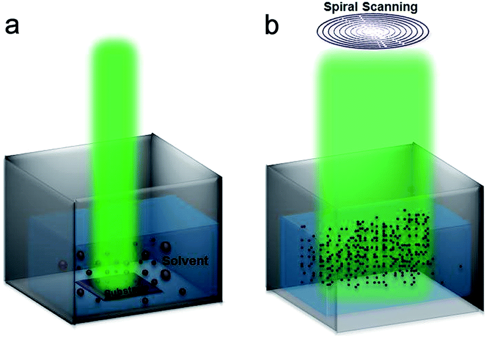 | ||
| Fig. 1 Schematic representation of NPs synthesis route by (a) stationary beam to produce large Si-NPs and (b) spiral beam to obtain ultra-small Si-NPs (∼3 nm). | ||
In this study, we have prepared 2 different NPs samples with high (60 mJ cm−2) and moderate (30 mJ cm−2) fluences. Both of these samples are obtained after 1500 loops of ablation under spiral scanning scheme. In this paper, these two types of NPs are recalled as blue and green NPs, respectively, due to their emission properties.
TEM images of as-prepared Si-NPs (200 loops) and those of ablated at different fluence levels for large number of loops (1500) are shown at Fig. 2a–f. From these images we can confirm that the obtained Si-NPs by laser ablation (200 loops) are nearly spherical with high size distribution (Fig. 2a). A shown in Fig. 2b, selected area electron diffraction pattern (SAED) of as-prepared NPs demonstrates that they are single crystalline, displaying (111) lattice sets with interplanar spacing of 0.31 nm (characteristic of Si bulk). As shown in Fig. 2d and f, this crystalline phase is not kept by green and blue NPs. For green NPs, a polycrystalline feature with several small grain boundaries can be observed while blue Si-NPs are amorphous. Also, as it can be seen from these figures, as-prepared NPs have a broad size distribution from tens to hundreds of nm. However, this distribution has been narrowed to much more uniform sizes with sub 5 nm dimensions for green (Fig. 2c) and blue (Fig. 2e) nanoparticles. These results are in line with a recent study that has investigated the formation of oxide layer around Si-NP during ablation process.29 This paper demonstrates that during laser ablation by nanosecond pulse, two types of morphologies can be formed for the nanocrystals; (1) a polycrystalline Si core surrounded with a thin SiOx shell, and (2) a fully oxidized amorphous SiOx. It has been also experimentally demonstrated that the latter case is likely when the temperature is high (above 1050 °C). This is in accordance with our findings that higher laser fluences can make higher local heating and initiate full oxidization. Although the exact mechanism of Si-NPs ablation in water solution is still debated, this process is generally explained in three phases:30–32 (1) laser induced heating, (2) adiabatic cooling and (3) resultant expansion. When the high intensity laser beam hits the Si, light is absorbed in the Si target and causes local heating (∼5000 K) where this heat is diffused into the bulk material by conduction, plasma formation and etc. Therefore, in the vicinity of the Si-NPs surface, generated NPs experience surface reconstruction due to laser induced heating and fast cooling. When this process continues for relatively large number of loops, this re-formed NPs get smaller and subsequently several deformations on the Si-NPs surface are created. In the dimensions as small as sub-5 nm, where surface properties start to be dominant over bulk ones, particles have already experienced multiple surface reconstructions. Therefore, the resultant morphology turns to polycrystalline one. Higher levels of fluence will make grain boundaries smaller and eventually the polycrystalline phase will turn to amorphous one as it is the case in blue Si-NPs.
 | ||
| Fig. 2 TEM images of Si-NPs obtained by nanosecond laser ablation prepared at different laser fluences; (a) as-prepared yellow Si-NPs and (b) their SAED pattern, (c) under 30 mJ cm−2 laser fluence ablated green Si-NPs and (d) its HRTEM image of individual Si-NP with high magnification interface, indicating 3.1 Å lattice fringes, and (e) 60 mJ cm−2 laser fluence used to synthesize blue Si-NPs and (f) its HRTEM image showing the amorphous nature of the resultant nanoparticles. | ||
Therefore, depending on the laser pulse fluence, these deformations can make polycrystalline or amorphous NPs. For high levels of laser fluence, in every ablation the grain boundary sizes decrease and finally at dimensions as small as 5 nm several ablation loops will make NPs to be amorphous.
To have a better comparison, Raman spectroscopy is utilized to evaluate NPs response in higher volumes rather than single nanoparticles (as we analyzed in TEM). Fig. 3 presents Raman responses for both blue and green Si-NPs. As revealed in this figure, both Si-NPs have two characteristic peaks; one is a sharp peak located at 515.8 cm−1 and the other is a broad peak extended toward 450 cm−1 with a weaker amplitude. Sharp peak is representing polycrystalline nature of NPs and the broad one is a sign of amorphous part. Therefore, by comparing these two peaks, we can find that the polycrystalline nature is dominant for green NPs while for that of blue NPs, amorphous portion is comparable with polycrystalline peak. Another feature that should be considered is the position of the polycrystalline peak which is downshifted by −4.2 cm−1 compared to reference bulk Si (520 cm−1). This shift proves the existence of quantum confined Si-NPs; the dependence of this peak shift (Δω) with Si-NPs size (D) can be explained by:33
| Δω = −52.3(0.543/D)1.586 |
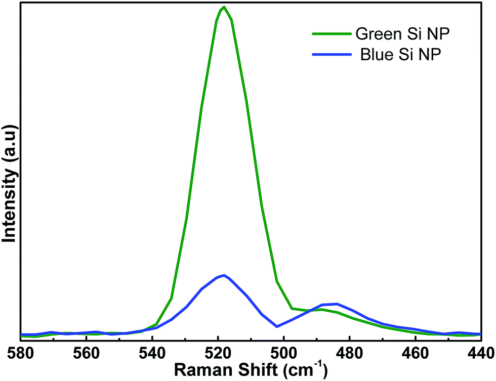 | ||
| Fig. 3 Raman spectra of the blue and green Si-NPs. | ||
Evaluating this equation with our measured values, we conclude that both blue and green NPs have the same estimated mean size of ca. 2.8 nm. Further investigations on NPs size and their optical response is conducted using UV-Vis-NIR spectroscopy, Fig. 4 represents absorption spectra of different sized Si-NPs. As it can be seen, larger sized Si-NPs (yellow ones) show an absorption edge in the near infrared (NIR) region which is inherent absorption of the bulk Si. This is expected considering the fact that generated Si-NPs have relatively large diameters (compared to ∼4 nm exciton Bohr radius of Si). However, the absorption edge of Si-NPs gets blue shifted due to quantum confinement effect. It is well known that when the sizes When dimensions of an indirect semiconductor approaches to dimensions as small as its exciton Bohr radius, it turns to a direct band gap semiconductor and experiences band gap widening. In our case, the band gap of NPs is calculated by extrapolation of the linear part of the (αω)1/2 versus hν axis in the wavelength range of 1–3 μm. These findings show that the corresponding band gaps for green and blue NPs are 1.59 eV and 1.64 eV, respectively. According to previous studies, the size of Si-NPs (with dimensions of 2–10 nm) can be estimated using below formula;34
| Eg = E0 + A × D−2 + B × D−1 |
 | ||
| Fig. 4 Optical absorption edge, (αω)1/2 as a function of photon energy (hν), measured from the nanoparticles; named with yellow, green and blue. | ||
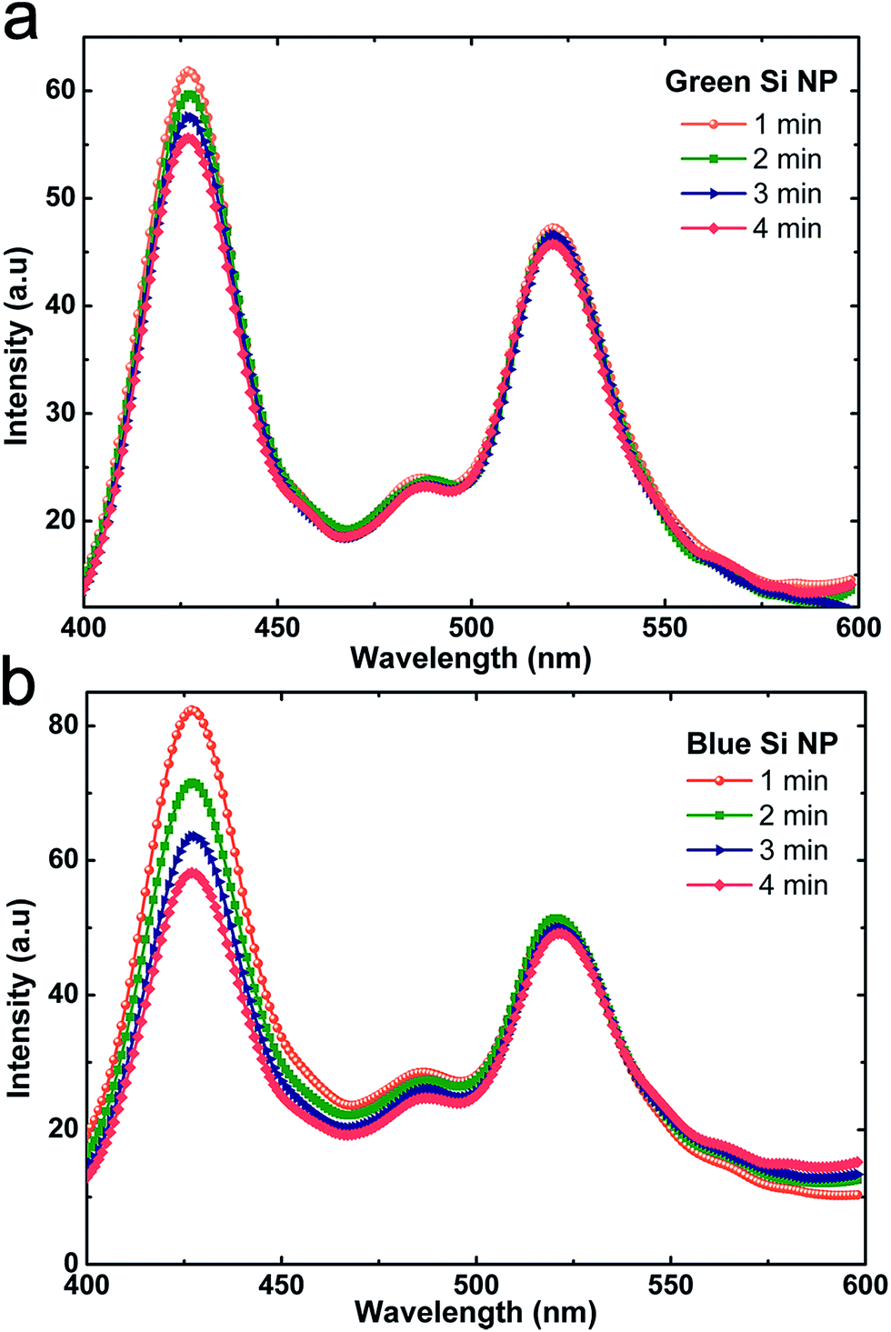
After all of these investigations that revealed both green and blue NPs have same size, photoluminescence (PL) spectroscopy is utilized to explore emission properties of Si-NPs. For this aim, PL spectra of Si-NPs under an excitation wavelength of 310 nm are recorded for both green and blue NPs. As it can be seen from Fig. 5, the emission for both of NPs is comprised of two main peaks located at 426 nm (blue emission) and 520 nm (green emission). However, the strength of these peaks is different for two solutions.
 | ||
| Fig. 5 PL spectra of blue and green Si-NPs excited at a wavelength of 310 nm. Inset shows intense visible (near red) luminescence under halogen lamp NPs before and after excitation. | ||
To have a better comparison, the ratio of PL (426 nm)/PL (520 nm) is calculated. Based on these results this ratio for blue emitting solution is about ∼1.85, while this amount is 1.33 for green one. The inset of the figure shows NPs before and after excitation with a halogen lamp (white light source with UV component). As indicated before, Si, as its bulk is an indirect band gap semiconductor with very weak emission property. However, when its dimensions shrink down, due to quantum confinement, the probability of direct transition will increase and consequently its emission yield is intensified. Thus, in our case, this emission could be a band-to-band transition as a consequence of quantum confinement effect. Also, due to existence of Si-NPs with different sizes, the emission should be tuned upon change in the excitation wavelength. So we repeated PL experiment with three different excitations; 290 nm, 310 nm, and 330 nm. As it can be clearly seen from Fig. 6a and b, moving toward higher excitation wavelengths for both solutions the blue emission at 426 nm gets a red shift which confirms the existence of quantum confinement effect in the solutions. Also, peak broadening in higher wavelength excited samples can originates from inhomogeneous broadening due to highly distributed defect states inside SiOx band gap.35 It has been shown that several defect states at different energetic locations are existed inside SiOx layer. According to the excitation wavelength, these states can be activated and even dominate the emission properties of the layer. It should be noted that the peak at 520 nm does not exhibit any shift which implies that these two peaks do not arise from the same origin. To have a better understanding on the origin of these two peaks, the impact of post-treatment by hydrofluoric acid (HF) on the PL emission of NPs is examined. For this aim, 5% HF is added to both blue and green emitting silicon NPs solution and PL emission of NPs is recorded in every 1 min intervals. Fig. 7a and b reveals that for both cases the blue peak (426 nm) is quenched after HF post-treatment while the green peak is almost unchanged. However, this quench is much more pronounced in the case of blue emitting NPs. Considering the fact that HF removes the SiOx layer by chemical etching, the reduction in the first peak (426 nm) can show us that this peak is mainly due to oxide related defects at Si/SiOx interface. This conclusion is in agreement with some of the previous studies where the blue emission is contributed to the defects at Si/SiOx interface29,36 rather than direct recombination in ultra-small (<5 nm) Si nanocrystals (due to quantum confinement). These studies show that the blue emission from Si nanocrystals is occurred at energy of 2.7 eV and this is mainly due to a forbidden triplet-to-singlet transition inside the SiOx shell layer. On the other side, the lack of any change for green peak (520 nm) represents that this emission stems from non-oxide related defects that are mainly grain boundaries at NPs surface. This fact can also be confirmed by comparing the decline strength for green and blue emitting NPs. The abrupt reduction for the case of blue emitting NPs reveals that the oxide related defects are more pronounced compared to that of green NPs solution. This can also be confirmed by reviewing the laser ablation process. When the level of laser fluence exceeds some threshold level, oxide layer formation can be initiated during the NPs formation.
 | ||
| Fig. 6 PL spectra of (a) green and (b) blue Si-NPs with different excitation wavelengths. | ||
 | ||
| Fig. 7 The impact of hydrofluoric acid post-treatment on PL spectra of (a) green and (b) blue emitting Si-NPs. | ||
To have an insight on density and nature of these oxide defects, XPS measurement is also carried out for both solutions. Fig. 8a compares Si2p spectra for two different solutions. These spectra have been deconvoluted to 6 different Gaussian functions; (1) Si peaks (Si2p3/2 at 99.6 eV, Si2p1/2 at 100.2 eV) and SiOx peaks (Si2O at 100.6 eV, SiO at 101.7 eV, Si2O3 at 102.5 eV, SiO2 at 103.4 eV). As shown in Fig. 8b and c, the percentage portion of area under SiOx peaks is 85% and 74% for blue and green emitting Si-NPs, respectively. This confirms our hypothesis that the SiOx layer formation is more likely under higher levels of laser fluence. On the other hand, the portion of non-stoichiometric SiOx (x ≠ 2) part is 25% for blue emitting Si-NPs while this amount is 14% for green ones. This demonstrates that, for blue emitting Si-NPs, density of oxide related defects at Si/SiOx interface is higher compared to that of green NPs.
 | ||
| Fig. 8 Si2p XPS spectrum of (a) green and blue Si-NPs and (b and c) their corresponding fitting. The Gaussian peaks belong to; Si2p3/2 at 99.6 eV (red), Si2p1/2 at 100.2 eV (dark yellow), Si2O at 100.6 eV (Olive), SiO at 101.7 eV (navy), Si2O3 at 102.5 eV (pink), SiO2 at 103.4 eV (violet). | ||
4 Conclusions
In this work, we conducted a systematic analysis on the origin of green and blue emissions from Si-NPs synthesized directly into the water by employing nanosecond pulsed laser ablation of Si bulk target. For this aim, first, we introduced a new ablation methodology based on spiral line scanning that ensures formation of ultra-small (as small as ∼3 nm), highly uniform luminescent NPs. Since NPs get trapped in the active area using this scanning scheme, laser spot interacts and ablates them during every cycle of scanning. Thus, in a short time, very small size Si-NPs with highly uniformity can be attained. Furthermore, It was demonstrated that by controlling the laser fluence, the luminescense of Si-NPs can be tuned between blue and green. Although both types of Si-NPs had almost same dimensions, their crystallinity was different in which Si-NPs synthesized at 30 mJ cm−2 show polycrystalline nature while the ones ablated at 60 mJ cm−2 were amorphous. This difference can cause emission of Si-NPs to be tuned between blue and green. We found that the blue emission (at 426 nm) is dominated with defect states at Si/SiOx interface, while that of green one (at 520 nm) is originated from disorders at the grain boundaries of the polycrystalline Si-NPs. At the high levels of laser fluence, high local heating makes adiabatic melting/cooling and subsequently grain boundary sizes of polycrystalline Si get smaller. For large number of laser ablation cycles, material experiences multiple surface reconstructions which turns its polycrystalline nature to amorphous one as it is the case for blue emitting Si-NPs. Our findings and the proposed method can be expanded to other type of materials where tunable structural and optical properties can be attained by adjusting the laser power.Acknowledgements
This work was partially supported by the Scientific and Technological Research Council of Turkey (TUBITAK) under Grant Nos 112M004, 112E052, and 113M815. A. K. O. acknowledges support from the Turkish Academy of Sciences Distinguished Young Scientist Award (TUBA GEBIP), BAGEP Award and FABED Award.References
- H. Chang and S.-Q. Sun, Chin. Phys. B, 2014, 23, 88102 CrossRef.
- J. G. C. Veinot, Chem. Commun., 2006, 4160–4168 RSC.
- A. S. Heintz, M. J. Fink and B. S. Mitchell, Adv. Mater., 2007, 19, 3984–3988 CrossRef CAS.
- W. A. Su and W. Z. Shen, Appl. Phys. Lett., 2012, 100, 071111 CrossRef.
- R. Koole, E. Groeneveld and D. Vanmaekelbergh, Nanoparticles, 2014, 13–52 Search PubMed.
- Z. T. Kang, B. Arnold, C. J. Summers and B. K. Wagner, Nanotechnology, 2006, 17, 4477–4482 CrossRef CAS.
- H. Morisaki, F. W. Ping, H. Ono and K. Yazawa, J. Appl. Phys., 1991, 70, 1869–1870 CrossRef CAS.
- H. Tamura, M. Rückschloss, T. Wirschem and S. Vepřek, Appl. Phys. Lett., 1994, 65, 1537–1539 CrossRef CAS.
- C. M. Gonzalez and J. G. C. Veinot, J. Mater. Chem. C, 2016, 4, 4836–4846 RSC.
- E. J. Henderson, A. J. Shuhendler, P. Prasad, V. Baumann, F. Maier-Flaig, D. O. Faulkner, U. Lemmer, X. Y. Wu and G. A. Ozin, Small, 2011, 7, 2507–2516 CAS.
- R. K. Baldwin, K. A. Pettigrew, E. Ratai, M. P. Augustine and S. M. Kauzlarich, Chem. Commun., 2002, 1822–1823 RSC.
- J. R. Heath, Science, 1992, 258, 1131–1133 CAS.
- J. Zou, P. Sanelle, K. A. Pettigrew and S. M. Kauzlarich, J. Cluster Sci., 2006, 17, 565–578 CrossRef CAS.
- R. A. Bley and S. M. Kauzlarich, J. Am. Chem. Soc., 1996, 118, 12461–12462 CrossRef CAS.
- M. H. Nayfeh, N. Barry, J. Therrien, O. Akcakir, E. Gratton and G. Belomoin, Appl. Phys. Lett., 2001, 78, 1131–1133 CrossRef CAS.
- O. Akcakir, J. Therrien, G. Belomoin, N. Barry, J. D. Muller, E. Gratton and M. Nayfeh, Appl. Phys. Lett., 2000, 76, 1857 CrossRef CAS.
- L. Mangolini, E. Thimsen and U. Kortshagen, Nano Lett., 2005, 5, 655–659 CrossRef CAS PubMed.
- H. Takagi, H. Ogawa, Y. Yamazaki, A. Ishizaki and T. Nakagiri, Appl. Phys. Lett., 1990, 56, 2379–2380 CrossRef CAS.
- G. Ledoux, O. Guillois, D. Porterat, C. Reynaud, F. Huisken, B. Kohn and V. Paillard, Phys. Rev. B: Condens. Matter Mater. Phys., 2000, 62, 15942–15951 CrossRef CAS.
- M. Ehbrecht, B. Kohn, F. Huisken, M. Laguna and V. Paillard, Phys. Rev. B: Condens. Matter Mater. Phys., 1997, 56, 6958–6964 CrossRef CAS.
- P. Chewchinda and T. Tsuge, Jpn. J. Appl. Phys., 2013, 52, 120699 CrossRef.
- A. Hamad, L. Li and Z. Liu, Appl. Phys. A, 2015, 120, 1247–1260 CrossRef CAS.
- K. Abderrafi, R. G. Calzada, M. B. Gongalsky, I. Suarez, R. Abarques, V. S. Chirvony, V. Y. Timoshenko, R. Ibanez and J. P. Martinez-Pastor, J. Phys. Chem., 2011, 115, 5147–5151 CrossRef CAS PubMed.
- L. Vaccaro, P. Camarda, F. Messina, G. Buscarino, S. Agnello, F. M. Gelardi, M. Cannas and R. Boscaino, AIP Conf. Proc., 2014, 1624, 1–6 CrossRef.
- S. Alkis, A. K. Okyay and B. Ortaç, J. Phys. Chem. C, 2012, 116, 3432–3436 CAS.
- X. D. Pi, R. W. Liptak, J. Deneen Nowak, N. P. Wells, C. B. Carter, S. A. Campbell and U. Kortshagen, Nanotechnology, 2008, 19, 245603 CrossRef CAS PubMed.
- S. Yang, W. Li, B. Cao, H. Zeng and W. Cai, J. Phys. Chem. C, 2011, 115, 21056–21062 CAS.
- I. D. Rukhlenko, M. Y. Leonov, V. K. Turkov, A. P. Litvin, A. S. Baimuratov, A. V. Baranov and A. V. Fedorov, Opt. Express, 2012, 20, 27612–27635 CrossRef CAS PubMed.
- L. Vaccaro, R. Popescu, F. Messina, P. Camarda, R. Schneider, D. Gerthsen, F. M. Gelardi and M. Cannas, J. Appl. Phys., 2016, 120, 024303 CrossRef.
- V. Amendola and M. Meneghetti, Phys. Chem. Chem. Phys., 2013, 15, 3027–3046 RSC.
- Z. Yan and D. B. Chrisey, J. Photochem. Photobiol., C, 2012, 13, 204–223 CrossRef CAS.
- H. Zeng, X. W. Du, S. C. Singh, S. A. Kulinich, S. Yang, J. He and W. Cai, Adv. Funct. Mater., 2012, 22, 1333–1353 CrossRef CAS.
- S. Yang, W. Cai, H. Zhang, X. Xu and H. Zeng, J. Phys. Chem. C, 2009, 113, 19091–19095 CAS.
- X. Liu, Y. Zhang, T. Yu, X. Qiao, R. Gresback, X. Pi and D. Yang, Part. Part. Syst. Charact., 2016, 33, 44–52 CrossRef CAS.
- L. Skuja, J. Non-Cryst. Solids, 1998, 239, 16–48 CrossRef CAS.
- L. Vaccaro, L. Sciortino, F. Messina, G. Buscarino, S. Agnello and M. Cannas, Appl. Surf. Sci., 2014, 302, 62–65 CrossRef CAS.
Footnotes |
| † These authors contributed equally to this work. |
| ‡ Dr Okyay was with Bilkent University at the time of the study. |
| This journal is © The Royal Society of Chemistry 2016 |