
 Open Access Article
 This Open Access Article is licensed under a
 Creative Commons Attribution 3.0 Unported Licence
Large-area two-dimensional bismuth selenide crystals synthesized by solution-based control of the nucleation environment†
Mukul Pradhan‡
abc,
Intek Song‡ab,
Jinho Leeab,
Minkyung Leeab,
Chibeom Parka and
Hee Cheul Choi*ab
aCenter for Artificial Low Dimensional Electronic System, Institute for Basic Science (IBS), Pohang 37673, Republic of Korea. E-mail: choihc@postech.edu
bDepartment of Chemistry, Pohang University of Science and Technology (POSTECH), Pohang 37673, Republic of Korea
cDepartment of Chemistry, National Institute of Technology – Meghalaya, Shillong-793003, Meghalaya, India
First published on 1st November 2016
Abstract
Two-dimensional (2D) Bi2Se3 is one of the most studied nanomaterials in recent years because of its fascinating electronic properties. However, previous synthesis methods, especially solution-based methods, were not capable of growing laterally large 2D Bi2Se3 crystals (mostly up to a few micrometers), and thus its real application and in-depth study was practically impossible. In this communication, we report a simple, reliable two-step method to synthesize large (20–50 μm in the lateral diameter and 10–15 nm in the thickness) disks of Bi2Se3 in the presence of ethylenediamine-tetraacetic acid (EDTA) and chloride ion, where EDTA acts as a complexing agent with bismuth(III). Depending on the growth conditions, we obtained 2D Bi2Se3 crystals having either a flat or spiral surface. We have thoroughly characterized the morphology, crystal structures, and electrical properties of these new disks, and we also discussed a possible growth mechanism based on the control over the surface chemistry and the nucleation stage.
Two-dimensional bismuth selenide (2D Bi2Se3) has gained much attention in recent years due to rapidly growing interest in it in the physical science fields as a representative example of thermoelectric materials, topological insulators, etc.1–4 Further in-depth studies and the real application of 2D Bi2Se3 requires the preparation of laterally large yet vertically thin crystals of 2D Bi2Se3, which should be uniform in structure and stable under ambient condition as well. To achieve this, a number of growth strategies have been applied so far,5–9 and among them solution-phase synthesis holds great significance because of its superior cost effectiveness and simplicity. However, the previous reports on the solution-based strategies could not produce crystals having both large lateral diameter and uniform surface morphology, by which most of the structural and electrical property analyses are quite limited. Therefore, a novel solution-based strategy is required to maximize the anisotropy of growing crystals and to retain the cost effectiveness and simplicity of the synthesis method.
The anisotropy is native to the layered structure of Bi2Se3 itself. Each quintuple layer, or the five-atom-thick Se–Bi–Se–Bi–Se layer, consists of strong covalent bondings between Se and Bi, whereas the interlayer interaction is weak van der Waals interaction.10 Therefore, the lateral growth, which adds stronger covalent bondings, would be thermodynamically preferred to the vertical growth, and thus a sophisticated control of the reaction environment may allow the lateral growth of Bi2Se3 while the vertical growth is suppressed.
A number of approaches have been applied to deliberately control the local environment of the growing crystals in solution, and notable examples include the use of additional chemicals11–13 and the separation of the nucleation and growth processes14,15 In case of the former, capping agents such as chelating ligands and halide ions that may adsorb onto specific crystal facets, and they promote or suppress the growth along certain crystallographic directions over others. In case of the latter, the separate nucleation step provides chances to control the number and the crystal structure of the nuclei.16,17 Especially, the seed-mediated growth, where the crystal growth occurs on pre-grown nucleation seeds, has been successfully employed to the growth of noble metal nanostructures, such as Au, Ag, and Pt etc.18,19
Herein, we report a two-step process for the controlled growth of 2D Bi2Se3 crystals that have a very high aspect ratio (c.a. 20–50 μm in the lateral diameter and 10 nm in the thickness) by combining both chelating ligands and the seed-mediated growth. We first prepared a batch dedicated to the nucleation step, and chelating agents such as chloride anions and EDTA successfully controlled the reaction environment to yield small circular seeds of Bi2Se3 dispersed in solution. Then, a solution containing unreacted Bi and Se precursors is dropwise injected into the seed-containing solution so that the seeds continue to grow laterally. As a result, we achieved all of the high aspect ratio (over 3500), the precise control of the crystal size, and the high reproducibility; we believe that this is the first time to realize them in case of Bi2Se3, to the best of our knowledge. We found that the properties of our 2D Bi2Se3 crystals indeed match with those of the previously reported crystals.
Fig. 1a shows the graphical illustration of the experimental setup for our seed-mediated growth. At first, nucleation seeds are synthesized on the right batch. After the formation of seed, the precursor solution in the left batch, which has been kept at lower temperature to prevent early reaction, is slowly injected into the right batch. As a result, seeds on the right batch grow laterally, and their lateral diameter reaches mostly up to 20–50 μm with smooth, flat top surface (Fig. 1b). Where, one pot reaction without seed-mediated growth resulted in the formation of 15–20 μm crystals (Fig. S1†). In the absence of any of EDTA and Cl−, we cannot observe the significant increase of crystal size. Note that a lower concentration of chelating EDTA yields spiral structures rather than flat crystals (Fig. 1c), and the absence of EDTA results in small (less than a few micrometers) crystals (Fig. S1†), in accordance with the previous results. This implies that the chelating agent EDTA participates in the reaction to control the growth environment. For the detailed experimental part, please see the ESI† section. Though the exact mechanism of the action of chloride ion used for the increase of the aspect ratio of crystal is not clear, we found that the use of bromide or iodide ions, instead of chloride ions, failed to increase the aspect ratio of the crystals. Nonetheless from XPS measurement we can detect that halide ions were found on the surface of the nanoplates (Fig. S2†). That is, each kind of halide ions can be well adsorbed on the surface.
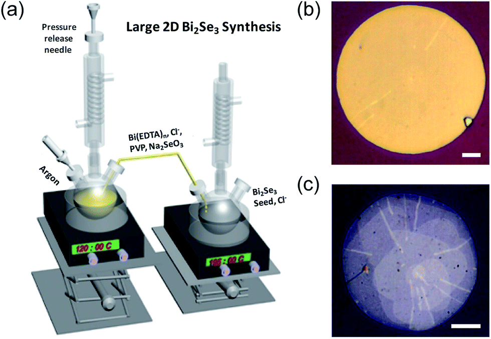 | ||
| Fig. 1 (a) Graphical illustration of the experimental setup for seed-mediated growth. (b) and (c) optical microscopic images of planar (b) and spiral (c) crystals, obtained at different EDTA concentration. All scale bars represent 5 μm. | ||
To characterize the obtained crystals, we performed Raman spectroscopy as shown in Fig. 2a. The sample was put on an SiO2/Si substrate for facile visualization (Fig. 1b and c), and we found three prominent peaks other than the Rayleigh peak at 0 cm−1. These peaks at 72, 131, and 174 cm−1 match with previously reported A1g, E2g, and A21g vibrational modes of Bi2Se3, respectively.20 Another prominent peak of Bi2Se3 is known to exist at 37 cm−1, but its energy is so close to the Rayleigh peak that our Raman spectrometer could not detect it. In addition, Raman spectroscopy mapping on an arbitrary crystal reveals that the number of the layers is uniform throughout the crystal.
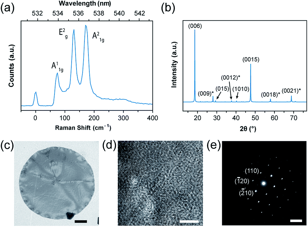 | ||
| Fig. 2 (a) A Raman spectrum of an arbitrary 2D Bi2Se3 crystal. (b) A powder X-ray diffraction pattern of 2D Bi2Se3 crystals. The asterisks denote that the marked peaks may overlap with other known diffraction patterns of 2D Bi2Se3. Also, all of the assigned peaks use the three indices system only; for example, (0012) states that the Miller index for the c axis is 12, not 2. (c) A transmission electron microscopic image of a grown crystal. The scale bar denotes 2 μm. (d) A high-resolution TEM image of the crystal and (e) its diffraction pattern. The scale bar of (d) represents 5 nm, and that of (e) denotes 5 nm−1. | ||
The powder X-ray diffraction pattern (Fig. 2b) of the crystal showed that the peaks overall match with typical rhombohedral Bi2Se3 crystals (JCPDS No. 33-0214). Since the pattern shows the strong intensity of the {003} family peaks, we assigned the prominent planar facet of the crystals as {001} planes. Such observation is cross-checked with transmission electron microscopy (TEM) measurement (Fig. 2c and d). High-resolution TEM (HRTEM) images show that the crystal structure has hexagonal lattice fringes with a correct lattice spacing of 2.1 Å between {110} planes. The diffraction pattern (the inset in Fig. 2d) exhibits clear the hexagonal symmetry of spots and single crystallinity; that is, the growth occurs along the 〈110〉 direction with {001} facets as the top and bottom surfaces. Also, we measured HAADF-STEM to obtain detailed microstructural information about the defect (Fig. S3†). We observed the polycrystalline nature of the defect site from HRTEM analysis (Fig. S4†). The rest of the crystal is more ordered and highly crystalline (Fig. S5†). FFT pattern and lattice spacing calculation also support the observation (Fig. S4 and S5†).
X-ray photoelectron spectroscopy (XPS) analysis of a three-day-old Bi2Se3 sample (Fig. S6†) shows that the sample is chemically Bi2Se3 with very small surface oxidation. However, it also reveals a minute trace of remnant reagents such as carbon of PVP, which may be removed by a simple thermal annealing process, and chlorine from the chloride anion (Fig. S6d and f†).21
In order to understand the roles of the chelating ligands and the seed-mediated growth, we intentionally controlled the reaction conditions. We found that if any of the nucleation seeds, EDTA and chloride ion is omitted, then the crystals grow to have non-uniform size distribution and a low aspect ratio (1–5 μm in the lateral diameter and 10–15 nm in the thickness) (Fig. S1†). That is, not only the chelating ligands, as we mentioned above, but also the nucleation seeds play crucial role in the crystal growth. In terms of the chelating ligands, the introduction of ammonium chloride and EDTA as complexing agents lead to the strong complexation with Bi3+, and the Bi-complexes slowly react with Se2− to produce a less number of nucleation seeds. Note that at this initial seed formation stage, we observed the presence of both elemental Se and Bi2Se3 by XPS (Fig. S7b†). With the reduced number of the nucleation seeds, the seed-mediated growth become more effective for the large-scale growth.
In order to understand the role of the seeds in the growth of large crystals, we performed time-dependent atomic force microscopy (Fig. 3) and optical microscopy observations (Fig. S8†). At the earlier stage of seeded growth, circular disks were formed, and they transform into hexagonal disks as their size increases. Also, the intermediate products obtained after 1.5 hours of reaction have huge particles on the surface of the crystals (Fig. 3a), but the surface becomes smooth at the late stage of the reaction. These observations imply that the lateral growth is substantially promoted without significant increase in the thickness; this is attributed to the presence of Cl− and EDTA–Bi strong complexation. We have provided the thickness distribution for the intermediate and final crystals (Fig. S9 and S10†).
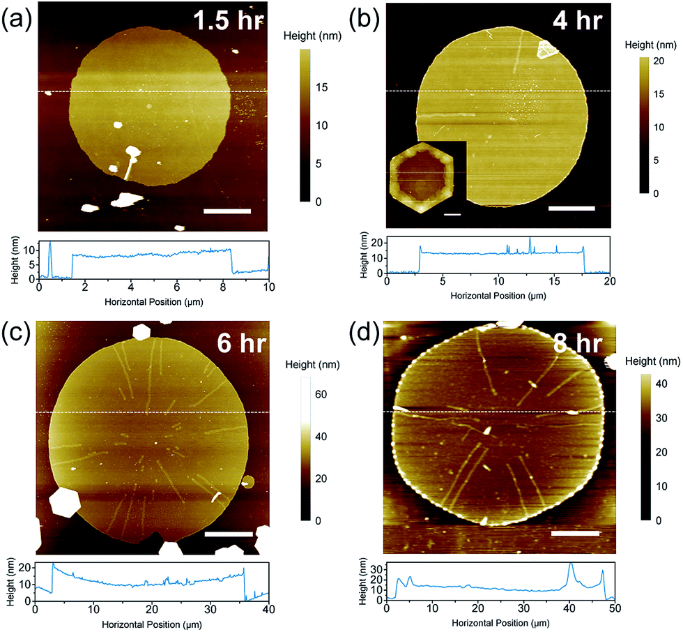 | ||
| Fig. 3 Atomic force microscopy images of Bi2Se3 crystals obtained at different reaction time: (a) 1.5 h, (b) 4 h, (c) 6 h, and (d) 8 h. The inset at (b) shows crystal obtained by adding the precursor solution at once. Here the scale bars all represent 5 μm. The graphs below the images show the height profile along the white dashed line. | ||
Another important factor for the successful large-scale growth is the control of the concentration of each reagent. For example, the drop wise addition of precursor solutions is necessary for the lateral growth; when the precursor solution was added to and mixed with the seed solution at once, the thickness of the edges of the crystals become much greater than that at the center (Fig. 3b, inset). In addition, a lower concentration of seeds results in the larger diameter of the final products, which may be explained by the low activation energy for the lateral growth relative to that of the separate seed formation.22 However, a further decrease of the seed concentration not only increases the lateral size of the growing crystals but also increases the possibility of the self-nucleation, because there is not much active site for further growth. Indeed, when the lateral diameter of the crystals become above 20 μm on average, small hexagons appear by self-nucleation, and thus the population of large crystals drops significantly. In principle, when large nanoplates grow, it is still possible to avoid the self-nucleation by further reducing the reaction rate by adding precursors more slowly. However, in practice, it is also important to keep a considerable reaction rate so that the desired dimension could be obtained within a reasonable period. Note that at relatively high precursor concentration, layer by layer (LBL) growth predominates as observed from the AFM study in Fig. S11.†
The electrical properties of Bi2Se3 crystals were investigated by fabricating field-effect transistors (FET). The optical microscope image in the inset in Fig. 4a shows a sample FET device fabricated by e-beam lithography (EBL). Note that we used LYRA3 FEG equipped with DrawBeam Advanced by TESCAN for all EBL. We used only Pd (50 nm) as source and drain electrodes, because it is known to significantly reduce the contact resistance compared to other typical sets of electrode metals such as Cr/Au or Ti/Au.4 All measurements were performed under Ar condition with low vacuum level (c.a. 1 torr). Temperature-dependent conductivity measurement shows that the sample is semiconducting as the conductivity decreases at lower temperature. Note that it also revealed that the sample is highly doped (i.e. formation of the donor levels), which may be attributed to chelating ions used during the synthesis reaction, such as chloride anions (Fig. S12†). To further investigate the semiconducting properties of the device, we conducted gate-dependence experiments. The IDS–VDS (VGS = 0 V) curve (Fig. 4a) shows that the curve is almost linear, showing that there is limited effect by Schottky contact between the electrode metal and the Bi2Se3 crystal. The IDS–VGS (VDS = 1 V) curves (Fig. 4b) show that the devices show n-type semiconducting behavior. The charge carrier mobility (μ) is estimated according to μ = (ΔIDS/ΔVGS) (L/W CoxVDS), where L and W are the channel length and width, and Cox is the capacitance of bottom gate oxide. The estimated charge carrier mobility for the synthesized Bi2Se3 disk is 68 cm2 V−1 s−1, which is comparable to that of the previous reports.23
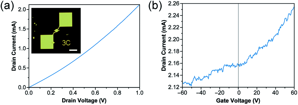 | ||
| Fig. 4 (a) IDS–VDS characteristics of the device (VGS = 0 V). The inset shows an optical microscope image of an FET device. The scale bar represents 50 μm. (b) IDS–VGS characteristics of the device (VDS = 1 V). | ||
In summary, 2D Bi2Se3 crystals with very high aspect ratios (up to 3500) have been successfully obtained through a two-step EDTA and Cl− ion-assisted, seed-mediated growth process at low temperature under reflux condition. We have observed the symmetry reduction for the morphology of the product through shape transformation during in situ seed-mediated synthesis of large 2D Bi2Se3. Presumably, by slowing down the reaction using Bi–EDTA complex as the precursor, we have successfully maintained the thickness about 10 nm for the 2D Bi2Se3 crystals with edge length up to c.a. 50 μm. We have synthesized 2D Bi2Se3 with single-grained as well as multi-grained crystals with stacked spirals by controlling the nucleation and growth process. Due to the large aspect ratio of the crystal, we easily fabricate FET device. We observed that synthesized Bi2Se3 shows decent room-temperature charge carrier mobility.
Acknowledgements
This work is supported by IBS-R014-G2 and NRF-2013K1A3A1A32035430. XPS measurements were performed at 8A1 beamline of the Pohang Accelerator Laboratory (PAL). Intek Song is grateful to Global Ph.D. Fellowship grant from NRF (NRF-2012H1A2A1016525).Notes and references
- Y. Min, J. W. Roh, H. Yang, M. Park, S. Il Kim, S. Hwang, S. M. Lee, K. H. Lee and U. Jeong, Adv. Mater., 2013, 25, 1425–1429 CrossRef CAS PubMed.
- L. Fu and C. L. Kane, Phys. Rev. B: Condens. Matter Mater. Phys., 2007, 76, 045302 CrossRef.
- D. Hsieh, D. Qian, L. Wray, Y. Xia, Y. S. Hor, R. J. Cava and M. Z. Hasan, Nature, 2008, 452, 970–974 CrossRef CAS PubMed.
- S. Cho, N. P. Butch, J. Paglione and M. S. Fuhrer, Nano Lett., 2011, 11, 1925–1927 CrossRef CAS PubMed.
- D. Kong, W. Dang, J. J. Cha, H. Li, S. Meister, H. Peng, Z. Liu and Y. Cui, Nano Lett., 2010, 10, 2245–2250 CrossRef CAS PubMed.
- D. Kong, J. C. Randel, H. Peng, J. J. Cha, S. Meister, K. Lai, Y. Chen, Z.-X. Shen, H. C. Manoharan and Y. Cui, Nano Lett., 2010, 10, 329–333 CrossRef CAS PubMed.
- Y. Min, G. D. Moon, B. S. Kim, B. Lim, J. S. Kim, C. Y. Kang and U. Jeong, J. Am. Chem. Soc., 2012, 134, 2872–2875 CrossRef CAS PubMed.
- L. D. Alegria, M. D. Schroer, A. Chatterjee, G. R. Poirier, M. Pretko, S. K. Patel and J. R. Petta, Nano Lett., 2012, 12, 4711–4714 CrossRef CAS PubMed.
- H. Li, J. Cao, W. Zheng, Y. Chen, D. Wu, W. Dang, K. Wang, H. Peng and Z. Liu, J. Am. Chem. Soc., 2012, 134, 6132–6135 CrossRef CAS PubMed.
- R. W. G. Wyckoff, Crystal Structures, Krieger, Malabar, FL, 1986 Search PubMed.
- X. Peng, L. Manna, W. Yang, J. Wickham, E. Scher, A. Kadavanich and A. P. Alivisatos, Nature, 2000, 404, 59–61 CrossRef CAS PubMed.
- V. Puntes, K. Krishnan and A. Alivisatos, Science., 2001, 291, 2115–2117 CrossRef CAS PubMed.
- Y. Sun, B. Mayers, T. Herricks and Y. Xia, Nano Lett., 2003, 3, 955–960 CrossRef CAS.
- Y. Xiong, I. Washio, J. Chen, M. Sadilek and Y. Xia, Angew. Chem., Int. Ed., 2007, 46, 4917–4921 CrossRef CAS PubMed.
- Y. Xia, Y. Xiong, B. Lim and S. E. Skrabalak, Angew. Chem., Int. Ed., 2009, 48, 60–103 CrossRef CAS PubMed.
- X. Peng, J. Wickham and A. P. Alivisatos, J. Am. Chem. Soc., 1998, 120, 5343–5344 CrossRef CAS.
- N. R. Jana, L. Gearheart and C. J. Murphy, Chem. Commun., 2001, 617–618 RSC.
- J. E. Millstone, G. S. Métraux and C. A. Mirkin, Adv. Funct. Mater., 2006, 16, 1209–1214 CrossRef CAS.
- S. E. Habas, H. Lee, V. Radmilovic, G. A. Somorjai and P. Yang, Nat. Mater., 2007, 6, 692–697 CrossRef CAS PubMed.
- W. Richter and C. R. Becker, Phys. Status Solidi B, 1977, 84, 619–628 CrossRef CAS.
- Y.-C. Hsueh, C.-C. Wang, C. Liu, C.-C. Kei and T.-P. Perng, Nanotechnology, 2012, 23, 405603 CrossRef PubMed.
- L. Carbone, C. Nobile, M. De Giorgi, F. Della Sala, G. Morello, P. Pompa, M. Hytch, E. Snoeck, A. Fiore, I. R. Franchini, M. Nadasan, A. F. Silvestre, L. Chiodo, S. Kudera, R. Cingolani, R. Krahne and L. Manna, Nano Lett., 2007, 7, 2942–2950 CrossRef CAS PubMed.
- Z. Lin, Y. Chen, A. Yin, Q. He, X. Huang, Y. Xu, Y. Liu, X. Zhong, Y. Huang and X. Duan, Nano Lett., 2014, 14, 6547–6553 CrossRef CAS PubMed.
Footnotes |
| † Electronic supplementary information (ESI) available. See DOI: 10.1039/c6ra23982j |
| ‡ These authors contributed equally to this work. |
| This journal is © The Royal Society of Chemistry 2016 |