Direct contact four-point probe characterization of Si microwire absorbers for artificial photosynthesis

J. T. Engelab, B. E. Blaikieab, A. Kumara, A. Castañedaa, A. Guptaa and D. R. Oliver*ab
aDepartment of Electrical and Computer Engineering, University of Manitoba, R3T 5V6, Winnipeg, Manitoba, Canada. E-mail: derek.oliver@umanitoba.ca
bManitoba Institute for Materials, University of Manitoba, R3T 2N2, Winnipeg, Manitoba, Canada

Received 21st September 2016 , Accepted 14th November 2016

First published on 14th November 2016


Abstract

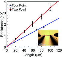
We present a facile approach that achieves four-point electrical characterization of silicon microwires fabricated using a bottom-up vapour–liquid–solid process. Tungsten probes are brought into direct contact with silicon microwires using piezoelectrically driven probe actuators. This technique can be applied to silicon microwires without the need for high-temperature lithographic preparation or the additional use of In/Ga to ensure reliable electrical contact between the probe and the wire. Comparison between two-point probe and four-point probe measurements demonstrates the robustness of the four-point approach. Significantly, the four-point characterization technique is not impacted by native oxides at the microwire/tungsten probe interface. The four-point technique can be applied to sense electrical responses in half-cell and full-cell representations of artificial photosynthesis systems, regardless of catalysts or functional groups attached to the microwire sidewalls.


Introduction

Since initial reports of water splitting as a consequence of light absorption by single semiconductor electrodes,1,2 there has been considerable discussion and interest in developing a working prototype that would utilize sunlight as the energy source.3–8 Artificial photosynthetic systems as proposed by Gray9 rely on the absorption of sunlight to split water, evolving hydrogen and oxygen.5,10 One realization of this approach incorporates two arrays of silicon microwire absorbers supported by a composite polymer membrane that is electrically and ionically conductive.5,6,10–12 In these designs, silicon microwires are grown “bottom-up” using a vapour–liquid–solid (VLS) chemical deposition process13,14 that has been adapted to produce highly crystalline nanowires15–17 and arrays of microwires18,19 for photovoltaic elements20,21 and water-splitting applications.22–24 In an operating water-splitting cell, the sidewalls of these absorbing elements would likely be functionalized to minimize oxidation of the surface, ensure efficient charge transfer at the microwire/polymer membrane interface and enable the attachment of catalysts.5,10,25–28

A two-point electrical measurement approach based on direct contact formation with the silicon microwires has previously been developed in response to the need to reliably characterize microwire doping concentration and microwire/polymer junction losses.29,30 This technique obviated the need for lithographic and other high-temperature processes associated with contact formation and has been demonstrated to produce high-yield contacts with equivalent results to contacts formed with the assistance of In/Ga.29 To establish ohmic contacts, local pressure > 11 mN μm−2 is required at the contact point to ensure a local phase transition in the microwire from Si-I to the metallic Si-IV phase.31–36 Although a lower threshold pressure (∼2 mN μm−2) has been shown to establish an effective electrical contact to the microwires,36 probe-microwire contacts with pressures in the range 2–11 mN μm−2 are not sufficiently ohmic to provide reliable two-point electrical measurements.29 During two-point electrical measurements, the range of resistance values obtained for each probe spacing reflected the consistency with which the two contacts were established.29–31 Removing surface oxides enhances this consistency: etching the microwires in buffered HF (aq.) prior to scraping them from the substrate and etching the tungsten probes in 2.0 M KOH for 30 s has been successfully employed.

Developing a working prototype of an artificial photosynthetic system requires the addition of molecular and/or inorganic species to the microwire sidewalls for oxidative stability and to promote oxygen- or hydrogen-evolving reactions.5,10,25–28 It has been shown that surface oxidation and/or functionalization significantly changes the electrical character of the microwire/membrane interface.10,25–27,29,30 Similar changes to the electrical character of the probe/microwire interface have the potential to inhibit the effectiveness of two-point based measurements. For sheet resistivities, four-point probe measurements are used to overcome this issue.37,38 Reported four-point contact electrical measurements of VLS-grown silicon microwires employ high-temperature lithographic processes to pattern the contacts.15,20,39–41 However these contact-formation processes are incompatible with candidate polymer membrane materials and/or the retention of functional groups attached to the microwire sidewall.29

We present a four-point probe approach to electrical characterization of silicon microwires (Fig. 1) that is unaffected by the degree of oxidation on the microwire sidewall, effectively overcoming this challenge.


image file: c6ra23534d-f1.tif
Fig. 1 The four-point probe measurement technique. (a) Optical micrograph with focal plane optimized to facilitate contact spacing measurement. Silicon microwire diameters were confirmed using scanning electron microscopy images. (b) Schematic diagram showing current-driving and sensing probes as connected to the semiconductor device analyzer (Agilent B1500A). The outer current-driving probes were always placed close to the ends of the Si microwire. The positions of the inner voltage-sensing probes were varied to achieve different probe separations and to confirm the consistency of measurements in different regions of the Si microwire.

Experimental

Sample preparation

Single-crystal n-type silicon microwires were grown on Si(111) substrates using the vapour–liquid–solid (VLS) chemical deposition process.25 Microwires produced for this work using this technique had a diameter of approximately 2 μm and lengths ranging from 40–150 μm and were predicted to have phosphorous doping concentrations in the range 1017 to 1018 cm−3. As in previous work, the microwire samples were etched in buffered HF (aq.) to remove surface oxides.10,29,30 Scraping a corner of the growth substrate with a razor blade removed microwires that were then suspended in acetonitrile (HPLC grade, Sigma Aldrich). Dispersion of the microwires was achieved by sonication for 5 min. A drop (∼10 μL) of the suspension was deposited onto a glass substrate, facilitating measurements on individual microwires.

Electrical measurements

Direct contacts were established using tungsten probes (2 μm tip radii, American Probe and Technologies) which had been etched for ∼30 s in 2.0 M KOH (aq.). The probes were controlled remotely via piezoelectrically driven units (Imina Technologies Micromanipulator miBot BT-11) housed in a standard probe station.
Two-point measurements. The two-point electrical measurements (Fig. 2) were obtained using a single pair of tungsten probes in contact with the microwires with a local pressure in excess of 11 mN μm−2. Multiple independent replications of the IV response for each probe spacing were obtained by disconnecting and re-establishing ohmic contact with the pair of probes.29,30
image file: c6ra23534d-f2.tif
Fig. 2 IV measurements obtained from a microwire via the two-point and four-point method for a given probe spacing. The two-point resistance indicated was chosen on the same basis as previous work.29,30 The resistance calculated for the four-point method used the entire data set. In the two-point method, the current is measured in response to voltage, while in the four-point method the voltage is measured in response to current.
Four-point electrical measurements. Electrical contact to a microwire was first established with the outer, current-driving, probes. The inner, voltage-sensing probes were then placed in contact with the wire and VI responses were obtained using an Agilent B1500A semiconductor parameter analyzer. Successful independent four-point electrical measurements were demonstrated by a hysteresis-free VI response (these axes have been transposed in Fig. 2 to facilitate comparison to the two-point measurements). Unsuccessful four-point contacts resulted in the presence of ∼0.5 V hysteresis in the neighbourhood I = 0. The hysteretic voltage response to the current sweep was attributed to charge trapping at one or more of the microwire/tungsten probe contacts. The capacitance associated with band-bending at a Schottky junction of this geometry traps sufficient charge to influence the voltage response on this order. The pressure required to remove this artefact is not sufficient to ensure contacts that would provide reliable two-point measurements. Nevertheless, successful four-point measurements, such as incorporated in Fig. 2, could be obtained from an intermediate local pressure regime (2–11 mN μm−2) in addition to the local pressure regime documented for the two-point electrical measurements (>11 mN μm−2).

Results and discussion

Multiple independent measurements for each probe spacing were obtained by completely disconnecting the probes from the microwire before re-establishing contact.29,30 Each data point in Fig. 3 is the average of between five and seven replicated measurements. For each replication, the success of a two point contact was confirmed by the self-consistency and linearity of the IV profile29,30 and the resistance calculated from the slope of the IV response.
image file: c6ra23534d-f3.tif
Fig. 3 Comparison of resistances from a single microwire measured using the four-point and two point methods at different probe spacings. The uncertainties (two-point data) represent the range of resistances averaged at each spacing. The range of resistances associated with the four-point probe replications are contained within the data points.

Regression analysis (Fig. 3) was used in conjunction with the two-point probe technique to estimate the contribution due to the microwire/tungsten probe resistance, 2Rc. The intercept (zero probe separation) predicted from regression analysis of the two-point probe measurements had an average value of 2Rc = 330 Ω and a range of 850 Ω. The corresponding average and range for the four-point probe measurements were 70 Ω and 100 Ω, respectively. These compare favourably with data reported in previous work.10,25,26,29–31 The physical “realization” of this value is less clearly-defined in the case of the four-point probe measurement where the intercept is expected to be negligible.

The smaller range in the replications of resistance (Fig. 3) and the greatly reduced standard deviation in the calculated doping concentrations (Table 1) demonstrate the reliability of the four-point approach.

Table 1 Microwire doping concentrations (Ndop, ×1017 cm−3) calculated from two-point and four-point resistance data.25,29–31 The error is the standard deviation for the values in each set
Wire Two-point Four-point
A 3.8 5.2
B 5.5 5.1
C 3.2 5.1
D 3.3 5.2
Average Ndop 4.2 ± 1.0 5.16 ± 0.05


It should be noted that each replicate four-point measurement is an independent measurement and can be used in a direct estimation of the doping concentration. Averaging n = 125 such estimates of the doping concentration may be calculated from these data (Table 2) with a corresponding standard deviation that better reflects the population of the data. For comparison, the doping concentration associated with the two-point measurements in Table 2 was extracted using a single regression line fitted to the complete set of data points (i.e. averages of replicated measurements).

Table 2 Microwire doping concentrations (Ndop, ×1017 cm−3) calculated from two-point and four-point resistance data obtained from four “as cleaned” wires. The error is the standard deviation in the values of doping concentration in each data set comprising n independent measurements
  Two-point Four-point
n 20 125
Ndop 4.0 ± 1.0 4.8 ± 0.3


The robustness of the four-point measurement technique was investigated by having two additional individuals estimate the probe separation. The probe and microwire diameters are both ∼2 μm, and the range of estimated doping concentrations calculated is greatly dependent on the operator's estimate of the probe separation. The images associated with each IV response curve were re-measured by the two additional operators to quantify the impact on both the standard error and average doping concentration. This expanded the set of four-point probe measurements for these “as cleaned” microwires to a population of n = 371 (Table 3).

Table 3 Microwire doping concentrations (Ndop, ×1017 cm−3) calculated from two-point and four-point resistance data obtained from four “as cleaned” wires (obtained at the same time as the two-point probe measurements) and four-point resistance data obtained from four “oxidized” wires that were scraped from the substrate after storage in ambient laboratory conditions for 12 months. The error is the standard deviation in the values of doping concentration in each data set comprising n independent measurements
  As-cleaned Oxidized
Two-point Four-point Four-point
n 20 371 240
Ndop 4.0 ± 1.0 4.6 ± 0.6 4.2 ± 0.4


After storage in ambient laboratory conditions for 12 months, a further set of wires were scraped from the substrate. Four-point probe measurements and calculations of the wire doping density were performed on four separate wires without native oxide removal from either the wires or the tungsten probes. In a similar approach to the “as cleaned” microwires, doping concentration data for these “oxidized” samples were compiled from measurements taken by three separate individuals, yielding a population of n = 240 measurements.

The error quoted in Table 3 most appropriately reflects the self-consistency of the four-point probe technique. A comparison between the “as-cleaned” and “oxidized” microwire data indicates that the four-point probe approach is insensitive both to the degree of native oxide present and the individual undertaking the measurements. Employing this approach, the limiting factor to an absolute determination of a VLS-grown microwire doping concentration is the measurement accuracy of the microwire diameter. We have shown that a small number four-point probe measurements provide sufficient accuracy for most microwire characterization purposes. This is a significant improvement in the rate at which microwire samples and associated half-cell structures can be tested/analyzed.

Conclusions

A facile four-point probe electrical measurement technique for characterizing the DC electrical characteristics of doped silicon microwires has been developed that can be employed without the use of high-temperature lithography or In/Ga contacts. These measurements are independent of the amount of native oxide present at the microwire/tungsten probe interface. This four-point probe technique measurement can be readily adapted to half-cell25,26,29 and full-cell10,30 representations of the artificial photosynthesis system9 that have been employed to characterize microwire/membrane junction behaviour.

Acknowledgements

Authors acknowledge financial support from Natural Sciences and Engineering Research Council (NSERC) of Canada. J. T. E., B. E. B. and A. K. acknowledge support from the Manitoba Institute for Materials. A. C. acknowledges support from Mitacs Globalink. A. G. acknowledges support from the Minister of Education and Advanced Learning, Manitoba. The work reported made use of surface characterization infrastructure in the Manitoba Institute for Materials that was funded through Western Economic Diversification (WED), Canada Foundation for Innovation (CFI), Canada Research Chairs Program, Manitoba Research and Innovation Fund, and University of Manitoba. The authors express their gratitude to O. S. Kang for assistance with the microwire fabrication.

Notes and references

  1. A. Fujishima and K. Honda, Nature, 1972, 238, 37 CrossRef CAS PubMed.
  2. J. Keeney, D. H. Weinstein and G. M. Haas, Nature, 1975, 253, 719 CrossRef CAS.
  3. M. Grätzel, Nature, 2001, 414, 338 CrossRef PubMed.
  4. N. S. Lewis, Science, 2007, 315, 798 CrossRef CAS PubMed.
  5. M. G. Walter, E. L. Warren, J. R. McKone, S. W. Boettcher, Q. Mi, E. A. Santori and N. S. Lewis, Chem. Rev., 2010, 110, 6446 CrossRef CAS PubMed.
  6. E. L. Warren, H. A. Atwater and N. S. Lewis, J. Phys. Chem. C, 2014, 118, 747 CAS.
  7. J. W. Ager, M. R. Shaner, K. A. Walczak, I. D. Sharp and S. Ardo, Energy Environ. Sci., 2015, 8, 2811 CAS.
  8. R. H. Coridan, A. C. Nielander, S. A. Francis, M. T. McDowell, V. Dix, S. M. Chatman and N. S. Lewis, Energy Environ. Sci., 2015, 8, 2886 CAS.
  9. H. B. Gray, Nat. Chem., 2009, 1, 7 CrossRef CAS PubMed.
  10. I. Yahyaie, S. Ardo, D. R. Oliver, D. J. Thomson, M. S. Freund and N. S. Lewis, Energy Environ. Sci., 2012, 5, 9789 CAS.
  11. K. E. Plass, M. A. Filler, J. M. Spurgeon, B. M. Kayes, S. Maldonado, B. S. Brunschwig, H. A. Atwater and N. S. Lewis, Adv. Mater., 2009, 21, 325 CrossRef CAS.
  12. M. B. McDonald, S. Ardo, N. S. Lewis and M. S. Freund, ChemSusChem, 2014, 7, 3021 CrossRef CAS PubMed.
  13. R. S. Wagner and W. C. Ellis, Appl. Phys. Lett., 1964, 4, 89 CrossRef CAS.
  14. R. S. Wagner, W. C. Ellis, K. A. Jackson and S. M. Arnold, J. Appl. Phys., 1964, 35, 2993 CrossRef CAS.
  15. Y. Cui and C. M. Lieber, Science, 2001, 291, 851 CrossRef CAS PubMed.
  16. Y. Cui, L. J. Lauhon, M. S. Gudiksen, J. Wang and C. M. Lieber, Appl. Phys. Lett., 2001, 78, 2214 CrossRef CAS.
  17. B. M. Kayes, M. A. Filler, M. C. Putnam, M. D. Kelzenberg, N. S. Lewis and H. A. Atwater, Appl. Phys. Lett., 2007, 91, 103110 CrossRef.
  18. V. Schmidt, J. V. Wittemann, S. Senz and U. Gösele, Adv. Mater., 2009, 21, 2681 CrossRef CAS.
  19. J. M. Spurgeon, K. E. Plass, B. M. Kayes, B. S. Brunschwig, H. A. Atwater and N. S. Lewis, Appl. Phys. Lett., 2008, 93, 032112 CrossRef.
  20. M. D. Kelzenberg, D. B. Turner-Evans, B. M. Kayes, M. A. Filler, M. C. Putnam, N. S. Lewis and H. A. Atwater, Nano Lett., 2008, 8, 710 CrossRef CAS PubMed.
  21. M. C. Putnam, S. W. Boettcher, M. D. Kelzenberg, D. B. Turner-Evans, J. M. Spurgeon, E. L. Warren, R. M. Briggs, N. S. Lewis and H. A. Atwater, Energy Environ. Sci., 2010, 3, 1037 Search PubMed.
  22. S. W. Boettcher, E. L. Warren, M. C. Putnam, E. A. Santori, D. Turner-Evans, M. D. Kelzenberg, M. G. Walter, J. R. McKone, B. S. Brunschwig, H. A. Atwater and N. S. Lewis, J. Am. Chem. Soc., 2011, 133, 1216 CrossRef CAS PubMed.
  23. A. C. Tamboli, C. T. Chen, E. L. Warren, D. B. Turner-Evans, M. D. Kelzenberg, H. A. Atwater and N. S. Lewis, IEEE J. Photovolt., 2012, 2, 294 CrossRef.
  24. E. L. Warren, H. A. Atwater and N. S. Lewis, J. Phys. Chem. C, 2014, 118, 747 CAS.
  25. J. P. Bruce, S. Asgari, S. Ardo, N. S. Lewis, D. R. Oliver and M. S. Freund, J. Phys. Chem. C, 2014, 118, 27742 CAS.
  26. J. P. Bruce, D. R. Oliver, N. S. Lewis and M. S. Freund, ACS Appl. Mater. Interfaces, 2015, 7, 27160 CAS.
  27. P. K. Giesbrecht, J. P. Bruce and M. S. Freund, ChemSusChem, 2016, 9, 109 CrossRef CAS PubMed.
  28. A. Gupta, J. P. Bruce, K. McEleney, M. S. Freund and D. R. Oliver, RSC Adv., 2016, 6, 88239 RSC.
  29. I. Yahyaie, K. McEleney, M. Walter, D. R. Oliver, D. J. Thomson, M. S. Freund and N. S. Lewis, J. Phys. Chem. Lett., 2011, 2, 675 CrossRef CAS.
  30. I. Yahyaie, K. McEleney, M. Walter, D. R. Oliver, D. J. Thomson, M. S. Freund and N. S. Lewis, J. Phys. Chem. C, 2011, 115, 24945 CAS.
  31. M. M. McClarty, J. P. Bruce, M. S. Freund and D. R. Oliver, Appl. Phys. Lett., 2015, 106, 022107 CrossRef.
  32. J. Z. Hu, L. D. Merkle, C. S. Menoni and I. L. Spain, Phys. Rev. B: Condens. Matter Mater. Phys., 1986, 34, 4679 CrossRef CAS.
  33. R. Hull, Properties of Crystalline Silicon, IET, London, UK, 1999 Search PubMed.
  34. J. Bradby and J. Williams, Phys. Rev. B: Condens. Matter Mater. Phys., 2003, 67, 085205 CrossRef.
  35. S. Ruffell, J. E. Bradby, N. Fujisawa and J. S. Williams, J. Appl. Phys., 2007, 101, 083531 CrossRef.
  36. M. M. McClarty, MSc Thesis, University of Manitoba, 2014 Search PubMed.
  37. F. M. Smits, Bell Syst. Tech. J., 1958, 37, 711 CrossRef.
  38. S. M. Sze and K. K. Ng, Physics of Semiconductor Devices, John Wiley & Sons Ltd., New York NY, 2007 Search PubMed.
  39. B. Tian, X. Zheng, T. J. Kempa, Y. Fang, N. Yu, G. Yu, J. Huang and C. M. Lieber, Nature, 2007, 449, 885 CrossRef CAS PubMed.
  40. M. D. Kelzenberg, D. B. Turner-Evans, M. C. Putnam, S. W. Boettcher, R. M. Briggs, J. Y. Baek, N. S. Lewis and H. A. Atwater, Energy Environ. Sci., 2011, 4, 866 CAS.
  41. P. Zhang, P. Liu, S. Siontas, A. Zaslavsky, D. Pacifici, J.-Y. Ha, S. Krylyuk and A. V. Davydov, J. Appl. Phys., 2015, 117, 125104 CrossRef.

This journal is © The Royal Society of Chemistry 2016
Click here to see how this site uses Cookies. View our privacy policy here.