DOI:
10.1039/C6RA23476C
(Paper)
RSC Adv., 2016,
6, 105761-105770
Microstructural, electrical and carrier transport properties of Au/NiO/n-GaN heterojunction with a nickel oxide interlayer
Received
21st September 2016
, Accepted 23rd October 2016
First published on 24th October 2016
Abstract
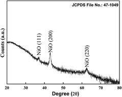
Nickel oxide (NiO) films are prepared on n-type GaN by an e-beam evaporation technique and its structural and chemical characteristics analysed by XRD, TEM and XPS measurements first at room temperature. XRD and TEM results reveal that the NiO films are oriented and that the NiO/n-GaN interface has a good quality. XPS analysis demonstrated that the NiO films clearly showed Ni 2p3/2 and 2p1/2 peaks at 854 eV and 872 eV along with the O 1s peak at ∼529.1 eV. Then, we fabricated an Au/NiO/n-GaN heterojunction Schottky diode with a NiO insulating layer and compared its electrical properties with the Au/n-GaN Schottky junction. The Au/NiO/n-GaN heterojunction presents excellent rectifying behaviour with a low reverse-leakage current compared to the Au/n-GaN Schottky junction. Calculation revealed that a higher barrier height is achieved for the Au/NiO/n-GaN heterojunction than for the Au/n-GaN Schottky junction, implying the barrier height was modified by the NiO insulating layer. Using Cheung's and Norde functions and an ΨS–V plot, the barrier heights are estimated and we found that the values are comparable with one another. The results suggest that the interface state density (NSS) of the Au/NiO/n-GaN heterojunction decreases compared to the Au/n-GaN Schottky junction, which indicates the NiO insulating layer plays a significant role in the reduced NSS. The results demonstrate that Poole–Frenkel emission governs the reverse leakage current in both junctions, which could be associated with structural defects and trap levels in the insulating layer.
Introduction
With the remarkable importance of III–V compound semiconductors, especially gallium nitride (GaN), they are eminently suitable semiconductor materials for the progress of metal/oxide/semiconductor field effect transistors (MOSFETS),1 heterojunction field effect transistors (HFET's)2 and high electron mobility transistors (HEMT's).3 To achieve such cutting-edge devices, metal/semiconductor (MS) junctions with an insulating or interlayer play a significant role in evaluating the performance, reliability and stability of the devices. Thus, one of the critical requirements for developing high performance Schottky devices is the specific restrain of insulator/interlayer in between the metal and semiconductor. Hence, it is challenging to obtain high-quality MS junctions with a low ideality factor by employing thin insulating or interlayer for electronic devices. The formation of a MS junction with an insulating layer on n-type GaN to obtain a low ideality factor, low reverse leakage current and high barrier height is critical, and thus to investigate the detailed electrical parameters of metal/insulator/n-GaN junction is essential. Some research groups have been motivated to form thin oxide/insulating layers in between the metal and GaN semiconductor, and investigated their electrical characteristics using different techniques.4–11 For instance, Oh et al.4 fabricated the AlGaN/GaN metal-oxide-semiconductor heterostructure field effect transistor using the NiO as a gate oxide and reported that the gate leakage current significantly decreased. Wang et al.5 demonstrated the electroluminescence properties of the NiO/n-GaN and NiO/MgO/n-GaN heterojunctions and reported that no emission was observed from the device without an MgO layer. Lalinsky et al.6 prepared AlGaN/GaN HEMTs with a thermic NiO gate contact layer and found that the NiO contact layer exhibited good dc performance with a larger gate voltage swing, high linearity and thermal stability compared to the Ni based gate contact layer device. Fiorenza et al.7 showed that the Poole–Frenkel mechanism controlled the current conduction through the NiO dielectric layer on a AlGaN/GaN heterostructure. Hui et al.8 fabricated a p-NiO/n-GaN heterojunction diode and found that the diode showed a typical rectifying nature with a turn-on voltage of about 2.2 V. Roccaforte et al.9 prepared the NiO layer on AlGaN/GaN heterostructures and observed that the leakage current was reduced with an interfacial NiO layer. Nigro et al.10 deposited NiO and CeO2 on AlGaN/GaN heterostructures and reported that the leakage current was reduced by 2–3 orders of magnitude for the NiO and 4 orders of magnitude for the CeO2. Li et al.11 fabricated a NiO/GaN heterojunction diode and found that the diode showed a relatively high turn-on voltage and lower leakage current.
Considering the above review, the present work is focused on the preparation and characterization of the Au/NiO/n-type GaN heterojunction Schottky diode by an e-beam evaporated thin nickel oxide (NiO) film as an insulating layer between the metal and GaN semiconductor. In this work, NiO is selected as an insulating layer for GaN devices, because of its band gap (3.6–4.0 eV) and quite high permittivity value (11.9).12 Also, NiO shows outstanding chemical stability, non-toxicity and function as a natural p-type direct-gap semiconductor.13 Further, NiO can be used in various applications, such as light emitting diodes,14 smart windows15 and chemical sensors16 due to its electrochromic, antiferromagnetic, low resistivity and UV optical transparency properties.17–19 In particular, NiO has comparable lattice constants and band gap energy to those of GaN; this makes NiO a favourable candidate for GaN-based heterojunction device applications. Therefore, we fabricated the Au/NiO/n-GaN heterojunction Schottky diode and characterized its microstructural, electrical and carrier transport properties. The electronic parameters of the heterojunction Schottky diode were also evaluated by different techniques (current–voltage, capacitance–voltage, Norde and Cheung's functions) and we correlated these parameters with the Au/n-GaN Schottky diode. In addition, the microstructural properties are correlated with the electrical results of the heterojunction diode. Finally, feasible carrier transport properties of the Au/n-GaN Schottky diode and Au/NiO/n-GaN heterojunction Schottky diode are also reviewed and discussed.
Experimental procedure
Si-doped GaN wafers (2 μm thick) (∼4.07 × 1017 cm−3) were used to fabricate metal/insulator/semiconductor heterojunctions and metal/semiconductor junctions. The n-type GaN wafer was grown on a sapphire substrate by a metal–organic chemical vapour deposition (MOCVD) technique. Prior to making heterostructures, the n-GaN wafer was cleaned with warm trichloroethylene, acetone and methanol for 5 min each by means of ultrasonic agitation. Then, the wafer was dipped into a buffered oxide etch (BOE) solution to remove the negative oxide on the surface of the wafer for 10 min followed by rinsing in deionized (DI) water. The outline of the circular geometry electrodes for the metal/insulator/semiconductor Schottky structures was made by using standard photolithography and lift-off techniques. After that, Ti/Al (30/100 nm) bilayer films were formed on the n-GaN substrate as ohmic contacts and annealed at 750 °C in N2 ambient for 1 min. Later, circular geometry electrode patterns were immersed into a BOE solution for 30 s and dried with N2 gas. Then, the nickel oxide (NiO) films were formed by electron beam (e-beam) evaporation on a cleaned n-GaN surface at a pressure of 8 × 10⁻⁶ Torr. The deposition rate of the NiO films is 1 Å s−1 with a substrate temperature of 303 K. The thickness of the NiO film was determined to be ∼70 nm by a transmission electron microscopy (TEM) method. Hall measurement results confirmed that the deposited NiO thin film has p-type conductivity. Next, a gold (Au) Schottky electrode was formed on NiO thin film by e-beam evaporation with a thickness of 30 nm under a pressure of 1 × 10⁻⁶ Torr. The circular diode area was 3.14 × 10⁻⁴ cm2. Now, the structure of the fabricated diode was an Au/NiO/n-type GaN heterojunction Schottky diode. Further, as a reference diode the Au/n-GaN Schottky diode was made without a NiO film layer on the same wafer. First, the quality of the deposited NiO thin films was assessed by X-ray diffraction (XRD). X-ray photoemission spectroscopy (XPS) and transmission electron microscopy (TEM) were also employed to characterize the microstructure of the heterojunctions. Finally, using an Agilent 4156C semiconductor parameter analyser and a 4284A precision LCR meter, the current–voltage (I–V) and capacitance–voltage (C–V) measurements of the Au/n-GaN reference diode and Au/NiO/n-GaN heterojunction Schottky diode were carried out at room temperature.
Results and discussion
Structural properties of nickel oxide (NiO)
The diffraction spectrum of nickel oxide (NiO) thin films deposited by an e-beam technique on n-type GaN is measured by glancing angle X-ray diffraction and is presented in Fig. 1. The peaks are observed at positions 37.26°, 43.23° and 62.54° assigned to the (111), (200) and (220) planes, respectively. However, the strongest peak is observed at 43.23° and all the peaks are indicated as per JCPDS no. 47-1049. The deposited NiO thin film has a cubic crystal system. The low peak intensity observed in the XRD spectra may be due to poor crystallinity. Further, no other phase peaks related to NiO occurred, which indicates the NiO films formed a stable phase. The preferential orientation peak (200) direction is observed in the deposited NiO films. The observed planes were well matched with reported planes in the literature.12,20 The cubic NiO thin films lattice parameter ‘a’ is evaluated for all peaks and an average lattice constant value is estimated. The lattice constant is estimated with the relation
, where h, k and l are Miller indices. The estimated average lattice constant value is 4.189 Å, which is somewhat larger than the standard value of 4.177 Å (from JCPDS no. 47-1049). The crystalline size of NiO thin films is calculated based on the Debye–Scherrer formula. It is found that the average crystalline size of the NiO film ranges from ∼8 to 12 nm. A similar crystalline size was also observed in sputtered NiO films reported by Chena et al.12 and Mahmoud et al.21 Transmission electron microscopy (TEM) analysis is also used to confirm the XRD analysis. The cross-section bright field TEM image achieved from the NiO/n-GaN heterojunction is presented in Fig. 2(a). The thickness of the NiO layer is estimated to be ∼70 nm. Also, Fig. 2(a) reveals excellent features of the interface between NiO and n-GaN, and observed is the crystallinity of the NiO on n-type GaN, which is consistent with the XRD results. Fig. 2(b) illustrates the EDX line profile of the NiO/n-GaN heterojunction, which indicates the presence of Ni, O, Ga, N and Au. This confirms that the interfacial layer is rich in Ni and O between the metal and n-GaN substrate. Normally, oxide layers that exist at the interface will lead to a rise in the contact resistance and decrease of the leakage current. This will be confirmed by current–voltage (I–V) measurements of the Au/NiO/n-GaN heterojunction later.
 |
| Fig. 1 XRD spectra of e-beam evaporated NiO thin films on n-type GaN. | |
 |
| Fig. 2 (a) STEM image acquired from the Au/NiO films on n-type GaN, and (b) EDX line profile spectra showing the element distribution across the junction. | |
The X-ray photoelectron spectroscopy (XPS) profile of the e-beam deposited NiO on n-GaN is represented in Fig. 3. The in situ etched NiO film XPS survey spectra are shown in Fig. 3. The C 1s carbon peak at 283.08 eV in the non-etched survey spectra is considered to correct the binding energies of all e-beam deposited NiO thin films. No contaminations are observed in all survey spectra. The binding energies of various etched survey spectra of NiO films are aligned and compared to the binding energy of fresh NiO film. In all the survey spectra, the presence of Ni, O and its satellite peaks along with Ga and the Ni substrate are observed. The carbon peak is observed only in the non-etched NiO film surface and is not seen after etching for 100 seconds. The Ni 2p3/2 and 2p1/2 are seen at nearly 854 eV and 872 eV, respectively, and the O 1s peak at ∼529.1 eV. Thus, all the detailed Ni 2p scans are recorded in the range of 846 eV to 882 eV and are represented in Fig. 4(a). From Fig. 4(a), both Ni2+ (2p3/2) and Ni3+ (2p3/2) are observed in both the etched and non-etched surfaces at 854.4 eV and 856.2 eV, respectively. However, for the in situ etched NiO surface, the peak intensities of Ni 2p1/2, and Ni 2p3/2 (Ni2+ and Ni3+) are decreased when compared to the fresh NiO film surface. These peaks almost disappear near the substrate surface, but the Ni0 (852.9 eV)22 peak intensity is increased towards the GaN substrate from the NiO film surface (Fig. 4(b)). The appearance of Ni0 in the e-beam deposited sample showed that the process parameter plays a vital role in forming the Ni0 defect in NiO films. The existence of the Ni0 state is accompanied with a decrement in the O 1s intensity at 530 eV, which showed the chance of oxygen vacancies in NiO films.23 This may be due to dissociation of the NiO molecule into Ni+ and O−. A typical single etched surface Ni 2p signal and its deconvoluted spectra are shown in Fig. 4(c). The Ni 2p might be deconvoluted into six peaks. The Ni 2p spectrum framed has two regions such as the Ni-2p3/2 (846–865 eV) and Ni 2p1/2 (865–882 eV) spin–orbit levels. The Ni 2p3/2 and Ni 2p1/2 are observed at 854.4 eV and 872.6 eV, respectively, along with their satellite peaks at 861.7 eV and 880.5 eV.24,25 Patel et al.26 also observed similar peak positions of Ni 2p in e-beam deposited NiO films. The NiO satellite peaks may arise due to various causes such as multi-electron excitations, multiple splitting or surface plasmon loss.27 The detailed in situ sputtered O 1s spectrum of the NiO film is recorded between 526 eV and 532 eV and is shown in Fig. 5(a). Also observed are two distinct peaks at nearly 529 eV and 527 eV. The O 1s higher binding energy peak at 292.1 eV is due to Ni2+ and the other one at 528.1 eV is due to Ni3+. The intensities of O 1s (Ni2+) and O 1s (Ni3+) are higher in a fresh NiO film surface compared to an in situ etching NiO film surface. The O 1s (Ni2+) of the NiO film shows a decrease in intensity compared to the O 1s (Ni3+) of the NiO film (Fig. 5(b and c)). The peaks are shifted towards the lower binding energy with in situ etching of NiO film surface (Fig. 5(c)). The Ni2+ ions oxidize to Ni3+ ions to maintain neutral charge.28 Therefore, the minimum quantity of surface energy is required to deposit high quality NiO films, and room temperature deposited films may have electron trap oxygen vacancy sites giving rise to Ni0 in NiO films.22
 |
| Fig. 3 XPS survey spectra obtained from the NiO film on n-type GaN deposited by electron beam evaporation. | |
 |
| Fig. 4 (a) Ni 2p XPS of NiO film after consecutive etched cycles, (b) typical Ni 2p XPS spectra without fitting, and (c) typical fitted curve for the Ni 2p spectrum. | |
 |
| Fig. 5 (a) O 1s XPS of NiO film after consecutive etched cycles, (b) typical fitted curve of the O 1s spectrum of fresh NiO film, and (c) typical fitted curve of the O 1s spectrum after a few consecutive etched cycles. | |
Electrical properties of the Au/n-GaN Schottky junction and the Au/NiO/n-GaN heterojunction
To correlate the NiO structural analysis with the electrical properties, we prepared an Au/NiO/n-GaN heterojunction Schottky diode with NiO as the insulating layer and Au/n-GaN as a reference Schottky junction. Fig. 6(a) shows the current–voltage (I–V) characteristic curves of the Ti/Al ohmic contacts on n-type GaN. It can be seen from Fig. 6(a) that the curve annealed at 750 °C shows linear behaviour that indicates good ohmic contacts are formed in the electrodes. The schematic heterojunction Schottky diode structure investigated in this work is represented in Fig. 6(b). Fig. 6(c) represents the reverse and forward current–voltage (I–V) characteristics of the Au/n-GaN Schottky junction and Au/NiO/n-GaN heterojunction Schottky diode in the voltage range from −3 V to +3 V. Excellent rectification behaviour is observed in the Au/NiO/n-GaN heterojunction Schottky diode as compared with that of the Au/n-GaN Schottky diode. The inset of Fig. 6(c) represents the I–V characteristics of Au/NiO/n-GaN heterojunctions with different thicknesses of NiO film, such as 40 nm, 70 nm and 100 nm. Measurements shows that the leakage currents of 40 nm, 70 nm and 100 nm are 1.218 × 10⁻⁸ A, 3.648 × 10⁻¹⁰ A and 1.919 × 10⁻⁹ A at −1 V, respectively. It is noted that a low leakage current is observed for the 70 nm thick NiO film as compared with that of the 40 nm and 100 nm thick NiO films. Therefore, the Au/NiO/n-GaN heterojunction fabricated with a 70 nm thickness of NiO film layer is mainly characterized in this work. Results indicate that a lower reverse leakage current (70 nm thick NiO film) is observed in the heterojunction (3.648 × 10⁻¹⁰ A at −1 V) compared to the reference diode (3.575 × 10⁻⁶ A at −1 V), implying the electrical properties of heterojunction diode are improved after placing a NiO layer in between metal and semiconductor. The barrier height and ideality factor of the Au/n-GaN Schottky junction and Au/NiO/n-GaN heterojunction are estimated by assuming thermionic (TE) theory39 and the respective values are 0.70 eV and 1.22, and 0.89 eV and 2.3, respectively. The result shows that the barrier height of both diodes rises in a forward bias which may be because of the increase in quasi-Fermi energy level of the majority of carriers on the GaN side. This causes the majority of the electrons to be injected straight into the metal making a thermionic current, though a few electrons are caught by the interface states, which results in an increase in barrier height and thus a decrease in the diode current.29,31 Also, the results presented show that the barrier height of the Au/n-GaN Schottky junction increases with the NiO insulating layer which may be due to an increase in negative charge at the junction. Presumably, the negative charges occur due to electron traps localized at the GaN interface which are related to Ga vacancies produced close to the surface at the time of creation of the insulating layer.32 Further, the ideality factors estimated are greater than one for both the Au/n-GaN Schottky junction and the Au/NiO/n-GaN heterojunction which may be due to different effects such as interface inhomogeneity, non-uniform distribution of the interfacial charges, the presence of surplus current and the recombination current by way of the interface states between the semiconductor and the interlayer.32,33
 |
| Fig. 6 (a) Display of the ohmic contact behaviour of Ti/Al electrodes on n-type GaN, (b) schematic diagram of the Au/NiO/n-GaN heterojunction and (c) reverse and forward current–voltage characteristics of the Au/n-GaN Schottky junction and the Au/NiO/n-GaN heterojunction measured at room temperature in the dark (inset: current–voltage curves of the Au/NiO/n-GaN heterojunction with different thickness of NiO layer). | |
The series resistance can play a critical role in the assessment of the electrical parameters of the heterojunction Schottky junction. The current–voltage (I–V) curves (see in Fig. 6) of the Au/n-GaN Schottky junction and the Au/NiO/n-GaN heterojunction express non-linearly at higher voltage regions which may be due to the series resistance (RS) and interface state density (NSS). However, the barrier height and ideality factor are substantial in linear and non-linear regions of the I–V curves. The barrier height, ideality factor and series resistance can be estimated by the technique proposed by Cheung from forward bias I–V curves. Cheung's functions are defined as34
|
 | (1) |
|
 | (2) |
Fig. 7 illustrates the dV/d(ln
I) versus I, and H(I) versus I plots derived from forward bias I–V curves of the Au/n-GaN Schottky junction and the Au/NiO/n-GaN heterojunction diodes. The dV/d(ln
I) versus I plot (Fig. 7(a) and (b)) shows a straight line from which the ideality factor and series resistance are estimated to be 2.36 and 40.36 Ω, and 2.91 and 676.84 Ω for the Schottky junction and heterojunction, respectively. Whereas, from the H(I) versus I plot (Fig. 7(a) and (b)), the barrier height and series resistance of the Au/n-GaN Schottky junction and Au/NiO/n-GaN heterojunction are found to be 0.72 eV and 40.44 Ω, and 0.94 eV and 850.17 Ω, respectively. Analysis showed that the series resistance values estimated by the Cheung's functions are closely concurrent with each other, which is evidence for the reliability of Cheung's approach. Calculation reveals that the series resistance value of the Au/NiO/n-GaN heterojunction is slightly higher than the value of the Au/n-GaN Schottky junction, because of the interfacial insulating layer that exists at the interface (as evidenced from TEM results). The ideality factors estimated from the dV/d(ln
I) versus I plot and linear region of the I–V curves are comparatively different from each other, which may be ascribed to the effects of series resistance and the bias credence barrier height along with the voltage drop across the interfacial layer and the modified interface states with bias in the downward-curvature region of the I–V curve.35,36 The modified Norde function was also applied to estimate and compare barrier heights of the Au/n-GaN Schottky junction and the Au/NiO/n-GaN heterojunction. Fig. 8 displays the Norde function F(V) versus V plot for the Schottky junction and heterojunction. The extracted barrier height and series resistance of the Au/n-GaN Schottky junction and the Au/NiO/n-GaN heterojunction are 0.71 eV and 226.12 Ω, and 0.88 eV and 6.99 kΩ, respectively. The barrier heights obtained from the Norde function are comparable to the values obtained from the I–V measurements.
 |
| Fig. 7 (a) Plot of dV/d(ln I) versus I and H(I) versus I for the Au/n-GaN Schottky junction, and (b) plot of dV/d(ln I) versus I and H(I) versus I for the Au/NiO/n-GaN heterojunction. | |
 |
| Fig. 8 Modified F(V) versus V plot for the Au/n-GaN Schottky junction and the Au/NiO/n-GaN heterojunction. | |
Moreover, the current through a metal/semiconductor with a negative oxide layer on the surface of the semiconductor is defined as
|
 | (4) |
where
A,
A*,
T,
k, and
n are the area of the diode, Richardson constant (26.4 A cm
−2 K
−2 for n-GaN
31), temperature in kelvin, Boltzmann's constant and ideality factor.
ΨS is the surface potential and is described as
|
 | (5) |
where
Vp is the potential difference between the Fermi level and the valence band maximum and
Vp = (
kT/
q)
![[thin space (1/6-em)]](https://www.rsc.org/images/entities/char_2009.gif)
ln(
Nc/
Nd), where
Nc is the effective density of the conduction band and
Nd is the carrier concentration and then
Vp can be estimated. Using
eqn (5),
ΨS is estimated by substituting the value of
Vp. The estimated
ΨS values
versus the forward bias voltage (V) are presented in
Fig. 9. From the
ΨS–
V plot, the critical surface potential,
ΨS(
IC,
VC), and the critical voltage
VC are obtained and then the barrier height can be estimated.
37 The barrier height,
Φb, is expressed by the following equation
|
Φb = ΨS(IC,VC) + αVC + Vp
| (6) |
 |
| Fig. 9 Surface potential versus forward voltage characteristics of the Au/n-GaN Schottky junction and the Au/NiO/n-GaN heterojunction. | |
It can be observed from Fig. 9 that the ΨS value reduces linearly up to V reaching the critical value VC. Further, α is the inverse of the ideality factor and is defined as
|
 | (7) |
Using eqn (6) and (7), the barrier height and ideality factor of the Au/n-GaN Schottky junction and Au/NiO/n-GaN heterojunction are determined to be 0.71 eV and 1.21, and 0.87 eV and 2.4, respectively. Analysis showed that the barrier heights determined by the forward-bias I–V, Cheung's and Norde functions and the ΨS–V plot are almost all similar values; hence the methods employed here have consistency and validity.
The schematic of the energy band diagram for a p-NiO/n-GaN heterojunction is presented in Fig. 10. The band gap (Eg) and electron affinity (χ) values for n-GaN and p-NiO are Eg,GaN = 3.4 eV, χGaN = 4.20 eV (ref. 38) and Eg,NiO = 3.86, χNiO = 1.46 eV,39 respectively. This can determine the differences in conduction band bottom and valence band top between n-GaN and p-NiO materials. The conduction band offset is ΔEC = χGaN − χNiO = 4.20 − 1.46 = 2.74 eV and the valence band offset is ΔEV = Eg,GaN − Eg,NiO + ΔEC = 3.40 − 3.86 + 2.74 = 2.28 eV. This shows a small valence band offset and a slightly larger conduction band offset.
 |
| Fig. 10 Schematic of energy band diagram of the p-NiO/n-GaN heterojunction. | |
Fig. 11 illustrates the 1/C2–V plot measured at 1 MHz for the Au/n-GaN Schottky junction and the Au/NiO/n-GaN heterojunction, from which the built-in potential and barrier heights are estimated. According to the Mott relationship between capacitance and voltage30,40 the built-in potential and barrier heights are found to be 0.83 V and 0.88 eV, and 1.23 V and 1.30 eV for the Schottky junction and heterojunction, respectively. It is found that the barrier heights calculated from the C–V method are higher than the values obtained by the I–V method; this may be due to the different nature of the C–V and I–V methods. Another possibility may be the existence of excess capacitance; the barrier heights are different. The differing barrier heights from the C–V and I–V techniques may be because of the effect of the image force and barrier inhomogeneities.41 Other reasons may be due to the defects in the interface, overruling insulating layer edge leakage current and deep impurity levels.42
 |
| Fig. 11 Plot of 1/C2 versus voltage (V) of the Au/n-GaN Schottky junction and the Au/NiO/n-GaN heterojunction. | |
Furthermore, the energy density distribution profiles of the Au/n-GaN Schottky junction and the Au/NiO/n-GaN heterojunction can be evaluated from the forward I–V data by taking account of the voltage-dependent ideality factor and effective barrier height. As suggested by Card and Rhoderick,43 the interface state density is described by
|
 | (8) |
where
n(
V) is the voltage-dependent ideality factor and is defined by
|
 | (9) |
where
εi is the permittivity of the interfacial layer,
εS the permittivity of the semiconductor,
δ the thickness of the interfacial layer and
WD the width of the space charge region. From high frequency (1 MHz)
C–
V data, the
WD is evaluated. In n-type semiconductors, the energy of the interface state density (
ESS) can be determined with regard to the conduction band at the semiconductor (
EC) surface and is defined as
|
EC − ESS = q(Φe − V)
| (10) |
Fig. 12 represents the NSS versus EC − ESS plot for the Au/n-GaN Schottky junction and Au/NiO/n-GaN heterojunction. As can be noted from Fig. 12, the NSS rises exponentially from the mid gap with regard to the bottom of the conduction band. The estimated NSS values are found in the range of 2.835 × 10¹⁴ (EC – 0.24 eV) to 4.008 × 10¹³ (EC – 0.65 eV) for the Au/n-GaN Schottky junction and 2.743 × 10¹² (EC – 0.23 eV) to 5.614 × 10¹¹ (EC – 0.88 eV) for the Au/NiO/n-GaN heterojunction. It is noticed that the two orders of NSS values of the heterojunction are lower than the Schottky junction, implying that the n-GaN surface is effectively passivated by the NiO insulating layer which means that the number of dangling bands decreases at the GaN surface as a result of the NSS. The NiO insulating layer decreases the saturation current in the heterojunction and raises the effective barrier height at the Schottky interface. As a result, it can be concluded that the NiO layer manipulates the NSS values.
 |
| Fig. 12 Plot of NSS versus EC − ESS curves of the Au/n-GaN Schottky junction and the Au/NiO/n-GaN heterojunction. | |
Next, the reverse leakage current mechanism in the Au/n-GaN Schottky junction and the Au/NiO/n-GaN heterojunction is investigated by considering either Poole–Frenkel emission (PFE) or Schottky emission (SE) mechanisms. The reverse current related to the Poole–Frenkel emission is defined as44,45
|
 | (11) |
and the Schottky emission is defined as
|
 | (12) |
where
βPF and
βSC are the Poole–Frenkel and Schottky field lowering coefficients, respectively. The theoretical values for
βPF and
βSC are described as
|
 | (13) |
where
q,
εr and
εo are the electric charge, relative permittivity of the semiconductor and the free space. At all times, the
βPF value is double the value of the
βSC. The assessed theoretical values of
βPF and
βSC are 2.461 × 10
−5 eV m
1/2 V
−1/2 and 1.230 × 10
−5 eV m
1/2 V
−1/2, respectively, for the Au/n-GaN Schottky junction and 2.199 × 10
−5 eV m
1/2 V
−1/2 and 1.099 × 10
−5 eV m
1/2 V
−1/2 respectively, for the Au/NiO/n-GaN heterojunction. A plot of ln(
IR)
versus (
VR)
1/2 drawn for the Schottky junction and heterojunction is represented in
Fig. 13. As can be seen in
Fig. 13, both the Schottky junction and the heterojunction exhibit linearity, which leads us to expect the reverse current being occupied by Poole–Frenkel or Schottky emissions for both junctions. By linear fitting of the ln(
IR)
versus (
VR)
1/2 plot the slope values determined are 2.989 × 10
−5 eV m
1/2 V
−1/2 for the Au/n-GaN Schottky junction and 4.037 × 10
−5 eV m
1/2 V
−1/2 for the Au/NiO/n-GaN heterojunction. The determined experimental slope values are found to be closer to the theoretical values of PFE compared to the SE regardless of the existence of the NiO interlayer. Therefore, the results suggest that the Poole–Frenkel emission governs the reverse leakage current conduction mechanism in both the Au/n-GaN Schottky junction and the Au/NiO/n-GaN heterojunction. In the PFE mechanism, the carrier transport happens from the metal into conductive dislocations
via trap states before direct emission from the metal.
44,46
 |
| Fig. 13 Plot of ln(IR) versus V1/2 for the Au/n-GaN Schottky junction and the Au/NiO/n-GaN heterojunction. | |
Conclusions
In summary, the nickel oxide (NiO) thin films are deposited by an e-beam evaporation technique on n-type GaN substrate and its structural and chemical properties reviewed by X-ray diffraction (XRD), transmission electron microscopy (TEM) and X-ray photoemission spectroscopy (XPS) measurements. XRD and TEM measurements show that the deposited NiO films on n-type GaN have a preferred orientation of NiO (200) and the NiO/n-GaN interface has a high quality. XPS results revealed that the peak intensities of Ni 2p1/2 and Ni 2p3/2 (Ni2+ and Ni3+) decreased when compared to the fresh NiO film surface and almost disappeared near the substrate surface. The O 1s (Ni2+) of the NiO film showed a decrease in intensity compared with the O 1s (Ni3+) of the NiO film and shifted towards the lower binding energy while in situ etching of the NiO film surface. Afterwards, the Au/NiO/n-GaN heterojunction Schottky diode is fabricated with NiO as an insulating layer between the metal and the n-GaN substrate, and we investigated its electrical and carrier transport properties at room temperature by current–voltage (I–V) and capacitance–voltage (C–V) methods. The heterojunction showed an excellent rectifying nature and low reverse leakage current as compared to the Au/n-GaN Schottky junction. A higher barrier height is obtained (0.89 eV (I–V) and 1.30 eV (C–V)) for the Au/NiO/n-GaN heterojunction than for the Au/n-GaN Schottky junction (0.70 eV (I–V) and 0.93 eV (C–V)). Also, the barrier height, ideality factor and series resistance are deduced by using Cheung's, Norde and the ΨS–V plot for the heterojunction and the Schottky junction. The barrier heights calculated by I–V, Cheung's, Norde and the ΨS–V plot are found to be comparable with each other, implying the methods used here are consistent and valid. The results indicate that the interface state density (NSS) of the Au/NiO/n-GaN heterojunction is lower than the Au/n-GaN Schottky junction, suggesting that the dangling bands on the surface of n-GaN are effectively reduced by the NiO insulating layer. Analysis of the results demonstrated that the reverse leakage current in both the Au/n-GaN Schottky junction and the Au/NiO/n-GaN heterojunction is ruled by a Poole–Frenkel emission. These analysis results are evidence that NiO films would be a preferable dielectric material in the fabrication of metal/oxide/semiconductor devices.
Acknowledgements
This research was supported by the Basic Science Research Program (NRF-2015R1A6A1A04020421) through the National Research Foundation of Korea (NRF) funded by the Ministry of Education, Republic of Korea, and by a grant from the R&D Program (Grant No. 10045216) for Industrial Core Technology funded by the Ministry of Trade, Industry and Energy (MOTIE), Republic of Korea.
References
- D. Mistele, T. Rotter, K. S. Röver, S. Paprotta, M. Seyboth, V. Schwegler, F. Edler, H. Klausing, O. K. Semchinova, J. Stemmer, J. Aderhold and J. Graul, Mater. Sci. Eng., B, 2002, 93, 107–111 CrossRef.
- J. D. Brown, R. Borgers, E. Pinner, A. Vescan, S. Sighal and R. Therrien, Solid-State Electron., 2002, 46, 1535–1539 CrossRef CAS.
- J. Moon, M. Micovic, A. Kurdoghlian, P. Janke, P. Hashimto, W. Wong, L. Mc Cray and C. Nguyen, IEEE Electron Device Lett., 2002, 23, 637–639 CrossRef CAS.
- C. S. Oh, J. Youn, G. M. Yang, K. Y. Lim and J. W. Yang, Appl. Phys. Lett., 2004, 85, 4214–4216 CrossRef CAS.
- H. Wang, G. Fang, H. Long, S. Li, X. Mo, H. Huang, H. Zhou and X. Zhao, Semicond. Sci. Technol., 2011, 26, 125015 CrossRef.
- T. Lalinsky, G. Vanko, M. Vallo, E. Dobrocka, I. Ryger and A. Vincze, Appl. Phys. Lett., 2012, 100, 092105 CrossRef.
- P. Fiorenza, G. Greco, F. Giannazzo, R. L. Nigro and F. Roccaforte, Appl. Phys. Lett., 2012, 101, 172901 CrossRef.
- W. A. N. G. Hui, Z. H. A. N. G. Bao-Lin, W. U. Guo-Guang, W. U. Chao, D. U. Guo-Tong and D. Xin, Chin. Phys. Lett., 2012, 29, 107304 CrossRef.
- F. Roccaforte, G. Greco, P. Fiorenza, V. Raineri, G. Malandrino and R. L. Nigro, Appl. Phys. Lett., 2012, 100, 063511 CrossRef.
- R. L. Nigro, G. Fisichella, S. Battiato, G. Greco, P. Fiorenza, F. Roccaforte and G. Malandrino, Mater. Chem. Phys., 2015, 162, 461–468 CrossRef.
- L. Li, X. Wang, Y. Liu and J.-P. Ao, J. Vac. Sci. Technol., A, 2016, 34, 02D104 Search PubMed.
- H.-L. Chen, Y.-M. Lu and W.-S. Hwang, Surf. Coat. Technol., 2005, 198, 138–142 CrossRef CAS.
- H. Sato, T. Minami, S. Takata and T. Yamada, Thin Solid Films, 1993, 236, 27–31 CrossRef CAS.
- J. M. Caruge, J. E. Halpert, V. Bulovic and M. G. Bawendi, Nano Lett., 2006, 6, 2991–2994 CrossRef CAS PubMed.
- E. L. Miller and R. E. Rocheleau, J. Electrochem. Soc., 1997, 144, 1995–2003 CrossRef CAS.
- X. F. Song, L. Gao and S. Mathur, J. Phys. Chem. C, 2011, 115, 21730–21735 CAS.
- D. A. Wruck and M. Rubin, J. Electrochem. Soc., 1993, 140, 1097–1104 CrossRef CAS.
- H. Yamane and M. Kobayashi, J. Appl. Phys., 1998, 83, 4862–4868 CrossRef CAS.
- P. Puspharajah, S. Radhaskrishna and A. K. Arof, J. Mater. Sci., 1997, 32, 3001–3006 CrossRef CAS.
- D. S. Dalavi, P. R. Jadhav, R. S. Deavn and P. S. Patil, Adv. Mater. Lett., 2015, 6, 99–103 CrossRef.
- S. A. Mahmoud, S. Alshomer and M. A. Tarawnh, J. Mod. Phys., 2011, 2, 1178–1186 CrossRef CAS.
- M. Tyagi, M. Tomar and V. Gupta, IEEE Electron Device Lett., 2013, 34, 81–83 CrossRef CAS.
- M. Tyagi, M. Tomar and V. Gupta, J. Mater. Res., 2013, 28, 723–732 CrossRef CAS.
- S. Oswald and W. Bruckner, Surf. Interface Anal., 2004, 36, 17–22 CrossRef CAS.
- W. C. Ching and Y. C. Fu, Nanoscale Res. Lett., 2013, 8, 33 CrossRef PubMed.
- K. J. Patel, M. S. Desai, C. J. Panchal, P. K. Mehta, I. M. Pazukha and I. Yu. Protsenko, Proceedings of the International Conference Nanomaterials: Applications and Properties, 2013, vol. 2, 01pcsi30(7pp) Search PubMed.
- J. M. Sanz and G. T. Tyuliev, Surf. Sci., 1996, 367, 196–202 CrossRef CAS.
- S. R. Jiang, P. X. Yan, B. X. Feng, X. M. Cai and J. Wang, Mater. Chem. Phys., 2002, 77, 384–389 CrossRef.
- E. H. Rhoderick and R. H. Williams, Metal-Semiconductor Contacts, Oxford, Clarendon Press, 1988 Search PubMed.
- A. Turut, M. Saglam, H. Efeoglu, N. Yalcin, M. Yildirim and B. Abay, Phys. B, 1995, 205, 41–50 CrossRef CAS.
- V. Rajagopal Reddy, M. Siva Pratap Reddy, B. Prasanna Lakshmi and A. Ashok Kumar, J. Alloys Compd., 2011, 509, 8001–8007 CrossRef.
- R. T. Tung, Phys. Rev. B: Condens. Matter Mater. Phys., 1992, 45, 13509–13523 CrossRef.
- D. T. Quam and H. Hbib, Solid-State Electron., 1993, 36, 339–344 CrossRef.
- S. K. Cheung and N. W. Cheung, Appl. Phys. Lett., 1986, 49, 85–87 CrossRef CAS.
- P. Prabhu Thapaswini, R. Padma, N. Balaram, B. Bindu and V. Rajagopal Reddy, Superlattices Microstruct., 2016, 93, 82–91 CrossRef.
- S. Karatas, S. Altindal, A. Turut and M. Cakar, Phys. B, 2007, 392, 43–50 CrossRef CAS.
- P. Chattopadhyay, Solid-State Electron., 1995, 38, 739–741 CrossRef CAS.
- T. Zhang, L. Li and J.-P. Ao, Surfaces and Interfaces, 2016, 5, 15–18 CrossRef.
- V. P. Sirkeli, O. Yilmazoglu, F. Küppers and H. L. Hartnagel, Semicond. Sci. Technol., 2015, 30, 065005 CrossRef.
- V. Rajagopal Reddy, V. Janardhanam, J.-W. Ju, H. Hong and C.-J. Choi, Semicond. Sci. Technol., 2014, 29, 075001 CrossRef.
- V. Rajagopal Reddy, D. Sri Silpa, V. Janardhanam, H.-J. Yun and C.-J. Choi, Electron. Mater. Lett., 2015, 11, 73–81 CrossRef CAS.
- S. M. Sze, Physics of Semiconductor Devices, Wiley, New York, 2nd edn, 1981 Search PubMed.
- H. C. Card and E. H. Rhoderick, J. Phys. D: Appl. Phys., 1971, 4, 1589–1601 CAS.
- A. Ashok Kumar, V. Rajagopal Reddy, V. Janardhanam, H. D. Yang, H.-J. Yun and C. J. Choi, J. Alloys Compd., 2013, 549, 18–21 CrossRef CAS.
- A. S. Raid, Phys. B, 1999, 270, 148–156 CrossRef.
- V. Rajagopal Reddy, V. Manjunath, V. Janardhanam, Y.-H. Kil and C.-J. Choi, J. Electron. Mater., 2014, 43, 3499–3507 CrossRef CAS.
|
This journal is © The Royal Society of Chemistry 2016 |
Click here to see how this site uses Cookies. View our privacy policy here.