DOI:
10.1039/C6RA23369D
(Paper)
RSC Adv., 2016,
6, 108621-108626
Nitrogen induced phosphorene formation on the boron phosphide (111) surface: a density functional theory study†
Received
20th September 2016
, Accepted 6th November 2016
First published on 7th November 2016
Abstract
Nitrogen induced phosphorene formation on top of the BP (111) surface is investigated using periodic density functional theory (DFT) calculations. We have considered adsorption/incorporation of different amounts of N, from 1/4 to 1 monolayer. Results demonstrate that the incorporation of a full N monolayer into the second P monolayer drives the formation of a P atomic wire at the surface. Adsorption of two monolayers on top of the phosphorus atomic wire results in the formation of a phosphorene atomic structure. Surface formation energy calculations indicate that for most of the allowed chemical potential range, the structure with the P zigzag atomic wire array is stable. However, for phosphorus rich conditions, the formation of a phosphorene configuration is also possible with almost the same formation energy. The phosphorene structure is bonded by van der Waals forces to the P atomic wire resembling the bilayer–bilayer distance in black phosphorus. From these results, it is clear that the N incorporation plays a key role in the stability and formation of phosphorene.
1. Introduction
The phosphorene, a two dimensional phosphorus material, has been the focus of active research due to its exceptional properties. In the same way as graphene is a single layer of graphite, phosphorene is a single bilayer of black phosphorus. Also, similar to graphite, in black phosphorus, P atoms are strongly bonded with other P atoms within the same bilayer, but consecutive bilayers are weakly bonded by van der Waals interactions.1 The electronic and thermal properties of phosphorene have been studied by several groups.2 Different from graphene, which is a zero gap material, phosphorene has a finite band gap.3 Due to quasi 1D band dispersions, this material exhibits a large exciton binding energy.4 Moreover, first principles calculations have been used to describe the thermal transport in phosphorene, finding an unprecedented anisotropy ratio.5
Phosphorene has some unique properties different from those of other two dimensional systems that makes it an interesting material for technological applications.1,6 For example, band gap engineering could be achieved with few phosphorene layers by varying the number of layers (phosphorene layers show a band gap thickness dependence).7 It has been demonstrated by experimental and theoretical methods that adsorption of metal adatoms on phosphorene layers enhances its thermal and structural stability.8 Also, Cai, et al.,9 have found an ultrafast mobility of the atomic vacancies at low temperatures. These findings improve the knowledge of phosphorene and open the possibility to use it in new technological applications. Therefore, phosphorene may be employed in the nano-electronic industry for the fabrication of field-effect transistors10 and optoelectronic devices.11,12
Likewise, it may be used as an electrode in the construction of lithium ion batteries.13 Other studies have proposed the use of phosphorene in the fabrication of gas sensor devices.14,15 It may also show photocatalytic activity by adjusting their energy gap to visible light adsorption by strain engineering.16 In the photo-voltaic industry, phosphorene may be employed as a donor material to construct solar-cells.17 It, also, may be doped with transition metals to construct diluted magnetic semiconductors, opening the possibility to apply it in the nano-spintronic industry.18,19
Phosphorene has been fabricated by mechanical20,21 and liquid phase22–24 exfoliation, but not by epitaxial growth, hindering its mass production, and therefore its possible applications.25 Then, in this paper, we report studies on the phosphorene epitaxial growth, driven by simple nitrogen incorporation into the PB (111) surface. The paper is organized as follows: Section 2 describes the methodology. Section 3 is devoted to summarize our findings, and finally, in Section 4 conclusions are made.
2. Method
Calculations were performed using periodic density functional theory, as implemented in the PWscf code of the Quantum ESPRESSO package.26 Exchange and correlation energies are modeled according to the generalized gradient approximation (GGA) with the Perdew–Burke–Ernzerhof (PBE) functional.27 Since, as mentioned before, two consecutive phosphorene layers are held together by van der Waals interactions, we have included the vdW-DF2 functional in the calculations to describe the phosphorene formation.28 Electron-ion interactions were treated with ultra-soft pseudopotentials.29 The electron wave functions are expanded in plane waves with kinetic-energy cutoff equal to 30 Ry and for the charge density 240 Ry. The BP zinc-blende structure was structurally optimized. Our results, compared with experiments and previous calculations, are summarized in Table 1.
Table 1 Lattice parameter comparison between theory (different approximations) and experiment
|
Exp ref. 30 |
Calculated (present work) |
Calculated ref. 31 |
Calculated ref. 32 |
a (Å) |
4.538 |
4.551 |
4.554 |
4.546 |
To model the BP (111) surface, a repeated slab geometry was used, with each slab consisting of four BP double layers with 2 × 2 surface periodicity (each layer is composed of four atoms) and the ad-atoms on top of the surface. Using the calculated lattice constant of the zinc blende BP structure we obtain the structural parameters of the BP (111) surface in a 2 × 2 periodicity. The parameters of the slab are:
,
, and c is equivalent to 10½ monolayers. Therefore, two consecutive slabs are separated by an empty space of ∼15.0 Å wide to avoid slab–slab interactions. The slab thickness was set to four BP bilayers. A Monkhorst–Pack mesh33 of 5 × 5 × 1 has been used to generate the k-points in the 2 × 2 unit cell (we have tested the convergency of the number of layers and number of k-points). Dangling bonds at the bottom surface were saturated using pseudo-hydrogen atoms with a fractional charge of 0.75e. The bottom BP bilayer and the saturating pseudo-H atoms were frozen at their ideal positions to simulate a bulk-like environment. To determine the most stable structure, the surface formation energy, which depends on the chemical potentials, is calculated for several atomic structures.
3. Results
3.1. Structural formation
3.1.1. Nitrogen adsorption on the BP (111) surface. The nitrogen adsorption on the BP (111) surface has been studied using a (2 × 2) surface cell and considering the adsorption at high symmetry sites:34 H3, T4, top, and bridge (Br). At the H3 site the N atom is above a phosphorus atom of the fourth layer, at the T4 site it is above a phosphorus atom of the second layer, at the top site it is placed on top of a B atom of the first layer, while in the bridge site it is placed between two boron atoms of the first layer. Total energy calculations obtained without van der Waals interactions indicate that the most favorable configuration corresponds to the H3 site. Therefore, this is considered as the reference configuration, and its energy is chosen as the zero value. The Br site shows a higher energy of 0.18 eV, the T4 site has an even higher energy of 0.52 eV, while the less stable configuration corresponds to the top site with an energy of 1.09 eV higher. A summary of the results is presented in Table 2.
Table 2 Relative energies without vdW interactions for the N adsorption on top of the surface, and incorporation into the BP (111) surface
Site |
N above (eV) |
First kind |
Second kind |
N-ML incorporation, P ML on top |
Site |
(eV) |
Site |
(eV) |
Site |
eV per N atom |
T4 |
0.52 |
T4-1 |
−2.31 |
T4-2 |
−0.03 |
ML-T4 |
2.05 |
H3 |
0.00 |
H3-1 |
−1.39 |
H3-2 |
1.42 |
ML-H3 |
2.87 |
Top |
1.09 |
TOP-1 |
0.23 |
TOP-2 |
2.01 |
ML-TOP |
2.43 |
Br |
0.18 |
|
|
|
|
ML-wire |
0.00 |
3.1.2. Nitrogen incorporation into BP inner layers. In this section, we have considered the possibility of the N incorporation into BP (111) inner layers. The nitrogen atom may occupy a site in the first bilayer by displacing a phosphorus atom. The P atom moves to the surface and becomes the new adatom. For this case two sets of high symmetry sites are possible. They are named as H3-1, T4-1 and TOP-1 for the first one, and H3-2, T4-2 and TOP-2 for the second.The H3-1 is a hollow site formed when the P atom bonds to three B atoms of the first monolayer; the N atom becomes a second nearest neighbor. The T4-1 is formed when the P adatom is at the T4 site, above a N atom of the second monolayer. In the TOP-1 site the adatom is placed on top of a first layer B atom that is forming bonds with two P and one N atom of the second layer. In set 2, the H3-2 is a hollow site in which the P atom bonds to three B atoms of the first monolayer. In this case the N atom becomes a third nearest neighbor. The T4-2 is a T4 site in which the P adatom is above a P atom of the second monolayer. In the TOP-2 site the adatom is placed on top of a first layer B atom that is forming bonds with three second layer P atoms.
It is noted that in set 1 the most stable geometry is the T4-1 site with an energy of −2.31 eV (taking as zero the energy of the H3 site), H3-1 has an intermediate energy of −1.39 eV, and the less stable structure corresponds to TOP-1 with an energy of 0.23 eV. Concerning to adsorption on set 2 sites, the most stable geometry is T4-2 with an energy of −0.03 eV, H3-2 has an intermediate energy of 1.42 eV, and the less stable structure corresponds to TOP-2 with an even higher energy of 2.01 eV. Therefore, we can conclude that when a N atom is incorporated into the second layer, by replacing the P atom, the most stable geometry for the displaced P atom corresponds to the T4-1 site. A summary of the relative energies is given in Table 2.
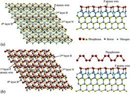
When the N coverage is 1 monolayer (ML), all N atoms occupy the original second layer of the surface. In the most stable structure a P zigzag atomic wire is formed on top, as seen in Fig. 1(a) (the top view is displayed at the left hand section and the side view at the right section). The zigzag atomic wire geometry can be clearly seen. Other configurations are less stable: a geometry with the displaced P atoms occupying Br sites is less stable by an energy of 0.67 eV per N atom, another configuration with the P atoms on T4 sites is even less stable by 2.05 eV per N atom. A P monolayer adsorbed on top sites has a higher energy of 2.43 eV per N atom, while a P monolayer adsorbed on H3 sites is the most unstable structure, having an energy 2.87 eV per N atom higher.
 |
| Fig. 1 (a) Top and side views of the nitrogen induced P atomic-wire and (b) top and side views of the phosphorene formation on top of the P atomic wire. | |
3.1.3. Phosphorene formation. Increasing the P coverage to a total of 3 ML results in the formation of a phosphorene layer on top of the phosphorus zigzag atomic wires, as shown in Fig. 1(b) (the top view is depicted at the left side and the side view at the right side).The side view shows clearly the formation of phosphorene. The structure is bonded to the P zigzag atomic wire with bond lengths of the same order as those of the black phosphorus structure. The inclusion of van der Waals forces is essential to correctly describe the atomic P wire-phosphorene interactions as well as the structural properties of the newly formed system.
3.2. Surface formation energy
Since the atomic structures considered in this study contain different number of atoms, the total energy is not an appropriate quantity to determine the most stable configuration. Instead, the surface formation energy (SFE), which is independent of the number of atoms, should be applied. The SFE can be written as:35,36
Ef = Eslab − Eref − μPnP − μBnB − μNnN |
where Eslab is the energy of the system under study, Eref is the reference energy, in this case the total energy of the ideal BP system, μi is the chemical potential of the i-th species, and ni is the excess or deficit of atoms at the surface. The formation energy is calculated as a function of the P chemical potential which should satisfy −ΔHPBf ≤ μP − μPbulk ≤ 0. The calculated BP formation enthalpy is ΔHPBf = μPBbulk − μPbulk − μBbulk = −0.913 eV. To carry out this analysis we have included van der Waals interactions in all the energetically stable configurations with different P and N content. In Fig. 2 we show the formation energy as a function of the phosphorus chemical potential. To explain Fig. 2, let us recall that the most stable structures have the lowest energies. Surface formation energies of the adsorption of 1/4, 1/2, and 3/4 N monolayers on the BP (111) surface can be seen as horizontal lines, with the configuration corresponding to the 1/4 monolayer being the less stable. As the N coverage increases the structure becomes more stable. At low chemical potentials (B-rich conditions) the surface formation energy indicates that the P atomic wire (induced by incorporation of a N monolayer) on top of the BP (111) surface represents the most stable geometry. As the P chemical potential increases towards P-rich conditions, the phosphorene structure becomes stable: its surface formation energy is almost the same as the surface formation energy of the P atomic wire structure, indicating that its formation is thermodynamically possible.
 |
| Fig. 2 Surface formation energy plot (in [eV/(1 × 1)]) considering van der Waals interactions. Comparison with the SFEs without vdW interactions is presented in Fig. S1.† | |
3.3. Structural properties of the phosphorene bilayers
In Fig. 3 we depict the phosphorene bilayers in order to compare the structural properties of the phosphorene epitaxially grown on BP (111) with the one obtained from black phosphorus and optimized using the same conditions as explained in the Method section.
 |
| Fig. 3 Phosphorene bilayers: (a) obtained from black phosphorus, and (b) epitaxial phosphorene grown on top of BP (111). | |
We can see from Table 3 and Fig. 3 that the structural parameters of the epitaxial phosphorene have an overall agreement with other experimental and theoretical results, except from the c parameter, that is larger. From Fig. 3 we note that phosphorene epitaxially grown on BP (111) (Fig. 3(b)) is elongated (with respect to the one obtained from black phosphorous) to be able to match the lattice parameter of the substrate BP (111) surface. This elongation is responsible for the larger c value. However, this elongation does not modify the overall structure of the phosphorene bilayer. Differences in the electronic properties are discussed in the following section.
Table 3 Structural parameters of the epitaxial phosphorene (grown on BP) and phosphorene bilayer
|
Epitaxial calc. |
Calculated |
Theo ref. 16 |
Exp ref. 37 |
Exp ref. 38 |
a (Å) |
3.23 |
3.32 |
3.30 |
3.27 |
3.31 |
c (Å) |
5.56 |
4.56 |
4.63 |
4.37 |
4.37 |
h1 (Å) |
2.20 |
2.23 |
2.22 |
— |
— |
h2 (Å) |
2.39 |
2.25 |
2.24 |
— |
— |
3.4. Electronic properties
Electronic properties are discussed in terms of the total density of states (DOS) and projected density of states (PDOS) of the two stable atomic geometries: the P zigzag atomic wire formation on top of the BP (111)-(1 × 1) surface and the phosphorene formation on top of the P atomic wire. To start the discussion let us first consider the ideally B-terminated BP (111) surface [Fig. 4(a)]. The total DOS is plotted as a function of energy with the reference being at the Fermi level. Since it is possible to observe a high population of states at and near the Fermi level, the BP (111) surface is clearly metallic.
 |
| Fig. 4 Total density of states of (a) the clean BP (111) surface, (b) the N-induced P atomic wire, and (c) the phosphorene bilayer formation on top of the P atomic wire. | |
3.4.1. DOS of the P atomic wire structure. Fig. 4(b) reports the total DOS and Fig. 5(a) the projected DOS of the zigzag atomic wire formed on top of the BP (111)-(1 × 1) surface. It is possible to observe states at and near the Fermi level, indicating a clear metallic behavior. Panel (a) of Fig. 5 shows the projected DOS corresponding to B, P and N s and p-orbitals, respectively. The main contributions at the Fermi level vicinities come from the p orbitals of the phosphorus atoms at the surface (P atomic wire atoms). Below the Fermi energy, the features of the DOS mainly come from the p orbitals of the B, N and P, with the most important contribution from the P atoms. For positive energies the DOS is dominated by the p orbitals of the B and P atoms.
 |
| Fig. 5 Orbital resolved projected density of states of (a) the P atomic wire, and (b) the phosphorene bilayer on top of the P-atomic wire. | |
3.4.2. DOS of the phosphorene structure. Fig. 4(c) shows the DOS of the phosphorene bilayer on top of the zigzag P wire. As in the other structures, the surface is metallic since there is no energy gap at the Fermi level. Fig. 5(b) shows the projected DOS of the B, P and N-s and p-orbitals. The B and N projected DOS are similar to those of the atomic P wire because they come from the same B and N atoms. However, since we now have more phosphorus atoms, the total DOS is slightly different: at energies above the Fermi level, the empty region in Fig. 4(b) almost disappears. This difference can be traced to the P p-orbitals.We finally discuss the effect of the elongation of the phosphorene bilayer in the electronic properties. We have calculated the density of states of an ideal phosphorene bilayer and compare it with the density of states of an elongated bilayer (see Fig. S2 in the ESI†). It is found that the density of states are very similar in both cases, but for the elongated phosphorene, the band gap is reduced, showing that band gap engineering can be achieved by straining the phosphorene, in good agreement with a previous report.16
3.5. Charge density
Charge density maps are also reported to show how the charge is distributed at the vicinities of the phosphorus zigzag atomic wire and phosphorene structure. Fig. 6(a) shows the charge density distribution corresponding to the phosphorus zigzag atomic wire formation on top of the BP (111)-(1 × 1) surface. Blue color is for low charge and white for high charge concentration. In this figure most of the charge is concentrated around each P atom. Also, two P nearest neighbors are sharing some charge, depicted as the green color between two P atoms, which in turn indicates formation of covalent bonds (we have to keep in mind that the P wire is slightly buckled, and therefore the P–P bond is not parallel to the BP surface, resulting in a lower charge density in the plotted plane). There is an asymmetry in the P wire with two different second nearest neighbor in-plane distances of 2.91 and 3.53 Å. Fig. 6(b) shows the charge distribution of the phosphorene layer on top. Again, most of the charge is concentrated around each P atom of the layer. There is also a charge density sharing between two P nearest neighbors, indicating in-plane covalent bonds, shown by the green color between a couple of P atoms. The phosphorene formation results in a more symmetric structure, with a second nearest neighbor in-plane distance of 3.22 Å. Moreover, reduced density gradient plots39 show charge density accumulation in the phosphorus–phosphorus bond region (Fig. S3†), supporting the above conclusions.
 |
| Fig. 6 Charge density plots of the stable structures: (a) the (0001) plane of the P atomic wire structure, and (b) the (0001) plane of the topmost phosphorene layer. The charge density has been plotted at the average height of the phosphorus wire and phosphorene layer, respectively. | |
4. Conclusions
First principles calculations, using periodic density functional theory, have been performed to investigate the nitrogen induced phosphorene formation on top of the BP (111)-(1 × 1) surface. We have found that it is energetically favorable for a nitrogen atom to incorporate into inner BP (111) layers, inducing the phosphorus atom to move to the surface. Increasing the coverage up to one monolayer results in the complete replacement of the topmost P layer by the nitrogen atoms, with the displaced P atoms forming a zigzag atomic wire on top. The deposit of two additional P monolayers results in the formation of a phosphorene atomic structure. The inclusion of van der Waals interactions is primordial to describe the thermodynamic stability of the different phases, as well as to describe their structural properties. It is found that the vertical separation between the P atomic wire and the phosphorene layer is similar to the one in black phosphorus.
Acknowledgements
G. H. C. acknowledges the financial support of VIEP-BUAP, grant HECG-EXC16-1, CONACYT project #83982, and Cuerpo Académico Física Computacional de la Materia Condensada (BUAP-CA-194). N. T. thanks DGAPA project IN100316 and CONACYT Project 164485 for partial financial support. Calculations were performed in the DGCTIC-UNAM supercomputing center project SC16-1-IG-31, Instituto de Física BUAP and LNS-BUAP.
References
- A. Castellanos-Gomez, J. Phys. Chem. Lett., 2015, 6, 4280 CrossRef CAS PubMed.
- T. Osada, J. Phys. Soc. Jpn., 2015, 84, 013703 CrossRef.
- V. Tran, R. Soklaski, Y. Liang and L. Yang, Phys. Rev. B: Condens. Matter Mater. Phys., 2014, 89, 235319 CrossRef.
- V. D. Ganesan, C. Zhang, Y. P. Feng and L. Shen, ArXiv: 1507.07343 [cond-mat.mtrl-sci], 2015.
- A. Jain and A. J. H. McGaughey, Sci. Rep., 2015, 5, 8501 CrossRef CAS PubMed.
- S. Bagheri, N. Mansouri and E. Aghaie, Int. J. Hydrogen Energy, 2016, 41, 4085 CrossRef CAS.
- A. N. Rudenko and M. I. Katsnelson, Phys. Rev. B: Condens. Matter Mater. Phys., 2014, 89, 201408 CrossRef.
- X. Feng, V. V. Kulish, P. Wu, X. Liu and K.-W. Ang, Nano Res., 2016, 9, 2687 CrossRef CAS.
- Y. Cai, Q. Ke, G. Zhang, B. I. Yakobson and Y.-W. Zhang, J. Am. Chem. Soc., 2016, 138, 10199 CrossRef CAS PubMed.
- L. Li, Y. Yu, G. J. Ye, Q. Ge, X. Ou, H. Wu, D. Feng, X. H. Chen and Y. Zhang, Nat. Nanotechnol., 2014, 9, 372 CrossRef CAS PubMed.
- R. Zhang, B. Li and J. Yang, J. Phys. Chem. C, 2015, 119, 2871 CAS.
- V. V. Kulish, O. I. Malyi, C. Persson and P. Wu, Phys. Chem. Chem. Phys., 2015, 17, 992 RSC.
- S. Zhao, W. Kang and J. Xue, J. Mater. Chem. A, 2014, 2, 19046 CAS.
- L. Kou, T. Frauenheim and C. Chen, J. Phys. Chem. Lett., 2014, 5, 2675 CrossRef CAS PubMed.
- N. Suvansinpan, F. Hussain, G. Zhang, C. H. Chiu, Y. Cai and Y.-W. Zhang, Nanotechnology, 2016, 27, 065708 CrossRef PubMed.
- B. Sa, Y.-L. Li, J. Qi, R. Ahuja and Z. Sun, J. Phys. Chem. C, 2014, 118, 26560 CAS.
- J. Dai and X. C. Zeng, J. Phys. Chem. Lett., 2014, 5, 1289 CrossRef CAS PubMed.
- X. Sui, C. Si, B. Shao, X. Zou, J. Wu, B.-L. Gu and W. Duan, J. Phys. Chem. C, 2015, 119, 10059 CAS.
- T. Hu and J. Hong, J. Phys. Chem. C, 2015, 119, 8199 CAS.
- S. P. Koenig, R. A. Doganov, H. Schmidt, A. H. Castro Neto and B. Ozyilmaz, Appl. Phys. Lett., 2014, 104, 103106 CrossRef.
- H. Liu, A. T. Neal, Z. Zhu, Z. Luo, X. Xu, D. Tomanek and P. D. Ye, ACS Nano, 2014, 8, 4033 CrossRef CAS PubMed.
- A. H. Woomer, T. W. Farnsworth, J. Hu, R. A. Wells, C. L. Donley and S. C. Warren, ACS Nano, 2015, 9, 8869 CrossRef CAS PubMed.
- Z. Guo, H. Zhang, S. Lu, Z. Wang, S. Tang, J. Shao, Z. Sun, H. Xie, H. Wang, X. F. Yu and P. K. Chu, Adv. Funct. Mater., 2015, 25, 6996 CrossRef CAS.
- J. R. Brent, N. Savjani, E. A. Lewis, S. J. Haigh, D. J. Lewis and P. O'Brien, Chem. Commun., 2014, 50, 13338 RSC.
- J. Gao, G. Zhang and Y.-W. Zhang, J. Am. Chem. Soc., 2016, 138, 4763 CrossRef CAS PubMed.
- P. Giannozzi, et al., J. Phys.: Condens. Matter, 2009, 21, 395502 CrossRef PubMed.
- J. P. Perdew, S. Burke and M. Ernzerhof, Phys. Rev. Lett., 1996, 77, 3865 CrossRef CAS PubMed.
- K. Lee, E. D. Murray, L. Kong, B. I. Lundqvist and D. C. Langreth, Phys. Rev. B: Condens. Matter Mater. Phys., 2010, 82, 081101(R) CrossRef.
- D. Vanderbilt, Phys. Rev. B: Condens. Matter Mater. Phys., 1990, 11, 7892 CrossRef.
- P. Popper and T. A. Ingles, Nature, 1957, 179, 1075 CrossRef CAS.
- A. Bouhemadou, R. Khenata, M. Kharoubi, T. Seddik, A. H. Reshak and Y. Al-Douri, Comput. Mater. Sci., 2009, 45, 474 CrossRef CAS.
- F. E. H. Hassan, H. Akbarzadeh and M. Zoaeter, J. Phys.: Condens. Matter, 2004, 16, 293 CrossRef.
- H. J. Monkhorst and J. D. Pack, Phys. Rev. B: Solid State, 1976, 13, 5188 CrossRef.
- J. Guerrero-Sanchez, J. Castro-Medina, J. F. Rivas-Silva, N. Takeuchi, L. Morales de la Garza, J. Varalda, D. H. Mosca and G. H. Cocoletzi, Z. Phys. Chem., 2016, 230, 943 CrossRef CAS.
- N. Takeuchi and S. Ulloa, Phys. Rev. B: Condens. Matter Mater. Phys., 2002, 65, 235307 CrossRef.
- N. Takeuchi, Phys. Rev. B: Condens. Matter Mater. Phys., 2002, 66, 153405 CrossRef.
- P. Yasaei, B. Kumar, T. Foroozan, C. Wang, M. Asadi, D. Tuschel, J. E. Indacochea, R. F. Klie and A. Salehi-Khojin, Adv. Mater., 2015, 27, 1887 CrossRef CAS PubMed.
- V. Sresht, A. A. H. Padua and D. Blankschtein, ACS Nano, 2015, 9, 8255 CrossRef CAS PubMed.
- J. Contreras-García, E. R. Johnson, S. Keinan, R. Chaudret, J.-P. Piquemal, D. N. Beratan and W. Yang, J. Chem. Theory Comput., 2011, 7, 625 CrossRef PubMed.
Footnote |
† Electronic supplementary information (ESI) available. See DOI: 10.1039/c6ra23369d |
|
This journal is © The Royal Society of Chemistry 2016 |
Click here to see how this site uses Cookies. View our privacy policy here.