
One-step synthesis of silver nanoplates with high aspect ratios: using coordination of silver ions to enhance lateral growth†
Young Min Park‡
a,
Byung Gon Lee‡a,
Jong-Il Weonb and
Mun Ho Kim*a
aDepartment of Polymer Engineering, Pukyong National University, 365 Sinseon-ro, Nam-gu, Busan 64547, Republic of Korea. E-mail: munho@pknu.ac.kr
bDepartment of Safety Engineering, Dongguk University, 707 Seokjang-dong, Gyeongju, Gyeongbuk 780-714, Republic of Korea
First published on 30th September 2016
Abstract
The single-step production of Ag nanoplates with high aspect ratios is of great significance for their applications to bendable or stretchable electrodes, but the development of a facile synthetic method remains a great challenge. In this paper, a coordination-based strategy was successfully employed to produce, in a single step, Ag nanoplates with high aspect ratios. Optimal Ag nanoplates were synthesized in the presence of acetonitrile, which served both as the co-solvent and as the ligand to form complexes with the Ag+ ions. Coordination effect of the Ag+ ions by acetonitrile apparently decreased the rate of the reduction of these ions, leading to a decrease in the number of seeds formed in the nucleation step. Decreasing the number of seeds in this way, while keeping the concentration of the Ag precursor constant, resulted in the formation of larger Ag nanoplates. This new synthetic method specifically enabled the formation of Ag nanoplates with lateral dimensions exceeding 1 μm and with thickness values of approximately 30 nm. These Ag nanoplates were found to show electrical percolation in a short sintering time and high electrical conductivity when they were directly used as metal inks to produce conductive patterns for printed electronics.
Introduction
Silver (Ag) nanoplates are two-dimensional anisotropic structures, i.e., with notably larger lateral than vertical dimensions, and exhibit fascinating plasmonic properties, such as intense quadrupole resonance peaks. Ag nanoplates have been intensively studied because of their potential utility in chemical and biological sensing.1,2 A number of different routes for synthesizing Ag nanoplates, including photo-induced transformation and chemical reduction of Ag+ in the presence or absence of seeds, have been demonstrated.3–9 The essential aspect of most of these syntheses is a slow rate of formation of Ag atoms to enable kinetic control of these reactions. Depending on the reduction rate, the final product can adopt a range of different shapes. For face-centered cubic (FCC) noble metals, cuboctahedra and multiply twinned particles (MTPs) have the lowest free energy and are therefore favored thermodynamically. To obtain a shape other than the thermodynamically determined morphology, the kinetics of nucleation and growth must be carefully controlled. Specifically, when the reduction is considerably slowed, the nanostructure growth is governed by the reaction kinetics rather than thermodynamics, thus enabling the formation of anisotropic nanostructures such as plates.10Since two-dimensional conducting nanosheets such as Ag nanoplates can be applied to the bendable or stretchable electrodes, the single-step production of Ag nanoplates have been of great interest. To reduce the percolation threshold for conductivity, Ag nanoplates with a high aspect ratio are preferred. However, in the kinetically controlled reaction conditions based on single-step synthetic methods, the lateral growth tends to cease after a certain amount of reaction time, preventing the formation of large Ag nanoplates. To our knowledge, most Ag nanoplates prepared from single-step synthetic routes based on solution-phase methods generally provide lateral sizes of less than 500 nm. In an effort to obtain Ag nanoplates with lateral sizes exceeding 1 μm, successive deposition procedures based on seed-mediated growth have shown success as alternative approaches.11,12 However, multistep deposition processes require a great deal of processing time and more continuous attention and effort than do the single-step reduction approaches.13
Here, we describe the development of a breakthrough approach yielding Ag nanoplates with high aspect ratios (i.e., having high ratios of lateral dimension to vertical dimension over 30) in a very high yield. In the new protocol, a coordination-based strategy was employed to produce Ag nanoplates with the extended lateral dimensions. The synthesis of the optimal Ag nanoplates was achieved by performing it in the presence of acetonitrile, which served both as the co-solvent and as the ligand of the Ag+ ions. It is well known that acetonitrile forms good coordination complexes with the Ag cation, specifically Ag(I). This new method enabled the formation of Ag nanoplates with lateral dimensions exceeding 1 μm and thickness values of approximately 30 nm. The procedure was quite simple because it produced Ag nanoplates via a one-pot synthetic method. A detailed study of the structural and morphological changes displayed during the growth of these Ag nanoplates was also carried out. Finally, conductive patterns were prepared by using these Ag nanoplates, the electrical resistivity of which was measured for their application as metallic inks for printed electronics.
Experimental section
Chemicals and materials
Silver nitrate (AgNO3, 209139, 100 g) and polyvinylpyrrolidone (PVP; Mw ≈ 10, and 29 kDa) were purchased from Aldrich (USA) and were used as received without further purification. N-Methyl-2-pyrrolidone (NMP; 74325, 1 L) and acetonitrile (34998, 2.5 L) were purchased from Aldrich (USA).Synthesis of Ag nanoplates
In a typical synthesis, 1.870 g PVP (Mw ≈ 29 kDa) was dissolved in 8 mL acetonitrile in a 20 mL vial (a liquid scintillation vial with a polyethylene liner and a white cap, Research Product International Corp.). Eight milliliters of the NMP solution containing AgNO3 (70.5 mM) were rapidly added to the vial using a glass pipette. In most of syntheses, the PVP-to-AgNO3 weight ratio in the total reaction mixture was fixed at 19.5. After capping the vial, the reaction was made to proceed by heating the mixture at 100 °C in air with magnetic stirring for 24 h. The final product was collected after centrifugation of the reacted mixture and was washed with DI water three times to remove most of the solvent and PVP. During the washing process, the suspension was centrifuged at 13![[thin space (1/6-em)]](https://www.rsc.org/images/entities/char_2009.gif) 000 rpm for 10 min. Finally, the precipitate was re-dispersed in DI water for use in subsequent characterization studies.
000 rpm for 10 min. Finally, the precipitate was re-dispersed in DI water for use in subsequent characterization studies.
Characterization
SEM images were recorded using a field-emission scanning electron microscope (Sirion, FEI) operated at an accelerating voltage of 10 kV. TEM images were obtained using a Philips Tecnai F30 microscope operated at 300 kV. The SEM (or TEM) sample was prepared by placing a drop of the final product (suspended in DI water) on a silicon wafer (or carbon-coated copper grid), and then drying the sample in a fume hood. The sample was then transferred to a gravity-fed flow cell and washed for 1 h with DI water to remove the remaining PVP. Finally, the sample was dried and stored in a vacuum. X-ray diffraction (XRD) data were recorded using a Philips 1820 diffractometer, and AFM images were collected on a Seiko SPA-400 with an SPI-3800 probe station. The surface resistance was measured by using a four-point probe measurement system (MCP-T610, Mitsubishi Chemical Analytech). Thermal decomposition analyses of the Ag nanoplates were carried out by using a thermogravimetric analyzer (TGA; Perkin Elmer, Pyris 1).Results and discussion
Polyvinylpyrrolidone (PVP) is nontoxic, highly chemically stable, and displays excellent solubility in a variety of polar solvents.14 PVP has been widely used in the synthesis of metal nanostructures as a steric stabilizer to prevent agglomeration and as a shape-control agent to promote the growth of specific crystal faces while hindering the growth of other faces.15 Recently, PVP has been shown to act as an ideal reducing agent, thanks to its weak reducing power, thereby enabling kinetic control over both nucleation and growth steps.15 The slow reduction of AgNO3 by the hydroxyl end groups of PVP is instrumental to the formation of Ag nanoplates.15–17 We recently reported a method for synthesizing Ag nanoplates in high yield using chemical reduction approaches.18,19 This method involved the reduction of AgNO3 by PVP in N-methyl-pyrrolidone(NMP). During the synthesis, PVP acted as a colloidal stabilizer and a weak reductant. In the NMP medium, the formation of Ag nanostructures with stacking faults was favorable, and the growth became kinetically controlled. However, the lateral growth tended to cease at a certain point of the reaction time, preventing the formation of large Ag nanoplates, and thus the average particle size (lateral dimension) of the obtained nanoplates was less than 250 nm.Being able to produce large Ag nanoplates is important in part because two-dimensional conducting nanosheets such as metal nanoplates have been of great interest, as they can be applied to bendable or stretchable electrodes for displays. To reduce the percolation threshold for conductivity, Ag nanoplates with high aspect ratios are preferred.20 Here, we report a new approach where Ag nanoplates with lateral sizes exceeding 1 μm can be obtained in a high reaction yield by simply introducing acetonitrile in the previous synthetic method.
In our new protocol, acetonitrile served both as a solvent and a ligand to form complexes with Ag+ ions. The coordination effect can substantially slow the reduction of Ag+ and consequently decrease the equilibrium concentration of elemental Ag(0), and hence lead to a suppression of the continuous formation of nucleation sites and a decrease in the number of seeds formed in the nucleation step.13,21 Such a decrease in the number of seeds, while keeping the concentration of Ag precursor constant, would be expected to result in the formation of larger Ag nanoplates. To investigate the growth of the Ag nanostructures in the presence of acetonitrile, we monitored the evolution of the shapes of these nanostructures by adding various amounts of acetonitrile as a co-solvent.
Fig. 1 shows TEM images of four samples of the syntheses that were carried out under the same conditions except for the ratio of acetonitrile to NMP in the reaction medium. In the synthesis, which was conducted at 100 °C, the PVP used had an average molecular weight of 29 kDa and its weight ratio to AgNO3 was kept at 19.5. In the absence of acetonitrile, only small nanoplates with dimensions of less than 200 nm appeared. As the acetonitrile-to-NMP ratio was increased from 0 to 0.5 and again to 1.0, the lateral dimensions of the obtained nanoplates were observed in both steps to increase markedly. These results indicated that acetonitrile dramatically affected the synthetic pathways by promoting an increase in the lateral dimensions of Ag nanoplates, and this increase was consistent with our expectations. A further increase of the acetonitrile fraction, however, did not lead to a further increase of the lateral dimensions. In fact, increasing the ratio of acetonitrile to NMP beyond 1.0 was found to negatively affect the growth of Ag nanoplates. This negative effect apparently resulted from the boiling temperature of acetonitrile being about 82 °C. Fig. S1† shows a TEM image of Ag nanoplates grown in pure acetonitrile at 80 °C. This image showed only relatively small nanoplates, none as large as those grown in the solvent mixtures with acetonitrile-to-NMP ratios of 1.0 or 1.5. The above results taken together showed that a high reaction temperature and a mixture of coordinating and noncoordinating solvents, specifically with equal volumes of acetonitrile and NMP, optimized the lateral growth of the silver particles. Plot of the lateral dimensions of the Ag nanoplates shown in Fig. 1 as a function of the volume ratio of acetonitrile to NMP is displayed in Fig. S2.†
 | ||
| Fig. 1 (A) TEM image of Ag nanoplates formed in the absence of acetonitrile. (B–D) TEM images of Ag nanoplates formed in the presence of acetonitrile. The volume ratios of acetonitrile to NMP were (B) 0.5, (C) 1.0, and (D) 1.5. The w/w ratio of PVP (29 kDa) to AgNO3 was 19.5. All syntheses were performed at 100 °C over a period of 24 h. | ||
Fig. 2A displays the X-ray diffraction (XRD) pattern recorded from the Ag nanoplates shown in Fig. 1A, i.e., grown in the absence of acetonitrile. The predominant peak in this pattern was at 38.2°, corresponding to the {111} plane. Low intensity of peaks were observed at 44.3° and 64.4°, corresponding to the {200} and {220} planes, respectively. The ratio of the intensity of the {111} diffraction peak to that of the {200} diffraction peak in this pattern was calculated to be about 8.5, considerably higher than the approximately 2.0 value of the ratio in the bulk material (JCPDS file no. 04-783).22 The Ag nanoplate surfaces presented {111} facets at the top and bottom surfaces, and each nanoplate edge consisted of a {111} facet and a {100} facet, each with a different size. The intensity ratio indicated that the top and bottom faces tended to be preferentially oriented parallel to the surface of the supporting substrate because of anisotropic features of the Ag nanoplates.23 For the Ag nanoplates, the ratio of the intensity of the {111} diffraction peak to that of the {200} diffraction peak was observed to increase as the average aspect ratio of the Ag nanoplates increased.
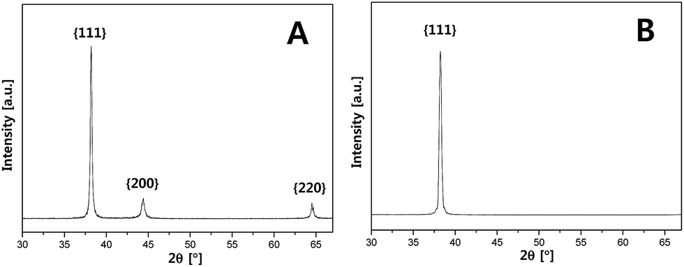 | ||
| Fig. 2 XRD patterns of the Ag nanoplates formed (A) in the absence of acetonitrile (sample shown in Fig. 1A and B) in the presence of acetonitrile (sample shown in Fig. 1B). | ||
Fig. 2B displays the XRD pattern of the Ag nanoplates shown in Fig. 1C that were grown in the presence of acetonitrile. Here, only the diffraction peak at 38.2° appeared in the spectrum, and this peak was quite intense. This result confirmed the extreme anisotropy of these Ag nanoplates, and confirmed that the growth of the lateral dimensions of the Ag nanoplates was highly promoted by introducing acetonitrile into the reaction mixtures.
In the synthesis of the Ag nanocrystals, the reaction can be readily followed based on the distinctive color changes that accompanied each stage in the reaction process.24 Injection of the AgNO3 solution into the PVP solution yielded a yellow solution, indicating the formation of silver nanoparticles. Heating at 100 °C induced a series of color changes, from brownish-yellow, to brown, and blue over the course of 1 h. The solution then passed through a series of color changes that included blue, dark blue, and blue-gray over a period of 24 h. When acetonitrile was added to the reaction, however, the system displayed relatively slow color changes, indicating that the nucleation and growth were impeded. Such a decreased rate of formation of nucleation sites may have resulted from Ag(I) ions reacting with the acetonitrile to form intermediate species, which may have served a reservoir to control the supersaturation of the Ag(I) ions in the solution. As a result, the reaction was significantly slowed down, which leads to suppression of continuous formation of nucleation sites. As a result, the number of nuclei formed by nucleation would be small. During the continuous reaction, nuclei evolved into seeds, and most of newly formed Ag atoms would have been expected to grow on the formed seeds. On the basis of the Gibbs–Thomson equation, slow reaction rates would have been expected to promote the growth of newly formed Ag atoms on the existing seeds, while fast reaction rates would have favored the self-nucleation process.12 Thus, in the presence of acetonitrile, the nanocrystals were able to grow into nanoplates with high aspect ratios as more Ag atoms were added to their edges.
However, in the absence of acetonitrile, many nuclei formed, apparently as a result of a sudden increase in the concentration of Ag atoms at the very early stages of the synthesis due to the relatively fast reduction of the AgNO3 precursor. Increasing the number of nuclei while keeping the concentration of the AgNO3 precursor in the reaction mixture constant has been shown to result in the production of small nanocrystals.25 A schematic illustration of the reaction pathways leading to the formation of Ag nanoplates with high aspect ratios is shown in Fig. 3.
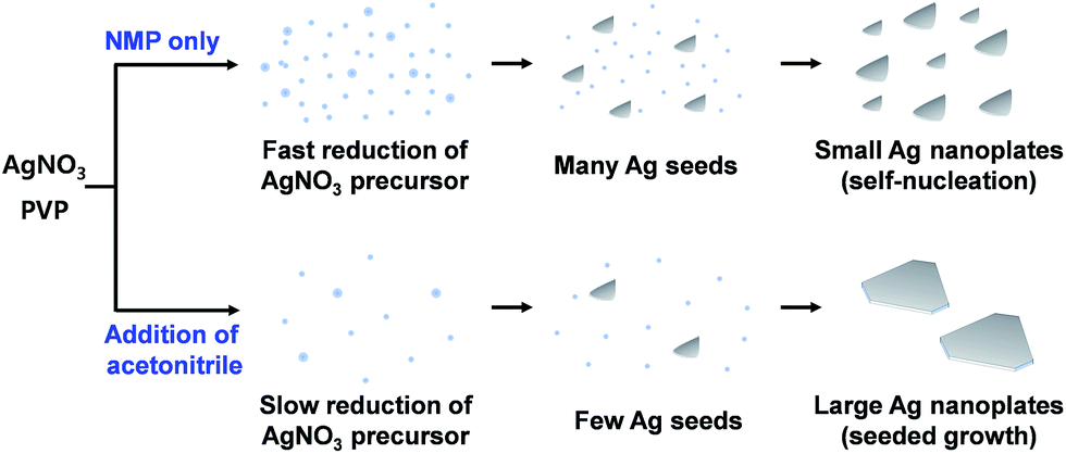 | ||
| Fig. 3 A schematic illustration of the reaction pathways that led to the formation of Ag nanoplates with high aspect ratios. | ||
The growth of the Ag nanoplates in the presence of acetonitrile was assessed by monitoring the evolution of their shapes. This monitoring was accomplished by conducting a series of reactions under identical conditions, stopping the reactions at various time points, and inspecting their TEM images (Fig. 4). The lateral dimensions of the nanoplates were observed to continue to increase with reaction time up to a reaction time of 24 h. In contrast, the lateral dimensions of the nanoplates were previously observed not to increase with the reaction time after 6 h of reaction in the absence of acetonitrile but otherwise using the same experimental conditions.18 Fig. 4A shows a TEM image of the nanoparticles grown in the presence of acetonitrile for 6 h. Most of the nanoparticles had plate-like structures with triangular and truncated triangular shapes. At this stage, the lateral dimensions of most of the nanoplates were less than 500 nm. As the reaction proceeded, small nanoplates below a certain size disappeared while the large nanoplates became bigger, suggesting an improvement of Ostwald ripening in the growth process.26 A considerable fraction of the nanoplates displayed a lateral size exceeding 1 μm after a reaction time of 24 h. The size distribution of the Ag nanoplates grown in the presence of acetonitrile for 24 h is shown in Fig. S3.† Fig. S4† shows AFM images of Ag nanoplates immobilized on a silicon wafer and the height profiles along the indicated lines. The average thickness of the nanoplates was found to be approximately 30 nm. Plot of the lateral dimensions of the Ag nanoplates shown in Fig. 4 as a function of reaction time is shown in Fig. S5.† When the reaction time was over 24 h, the notable changes in the lateral sizes and morphologies of Ag nanoplates were not observed. The nanoplate yield (the percentage of plates in the products) from this system was nearly 100%. In the presence of acetonitrile, the reduction rate was quite low and the nucleation and growth of the Ag nanoplates proceeded entirely under kinetic control. Therefore, most of the synthesized nanostructures assumed plate-like structures.
 | ||
| Fig. 4 TEM images of products sampled at reaction times of (A) t = 6 h, (B) t = 12 h, (C) t = 18 h, and (D) t = 24 h. The Ag nanoplates were grown in the presence of acetonitrile, and the volume ratio of acetonitrile to NMP was 1:1 (scale bar = 1 μm). The w/w ratio of PVP (29 kDa) to AgNO3 was 19.5. All syntheses were performed at 100 °C over a period of 24 h. | ||
The effects of acetonitrile on the reduction mechanism of Ag+ were also examined, by performing the reaction without the PVP reductant. In this case, the reaction proceeded very slowly, and the reaction mixture remained colorless for up to 3 h, indicating that while acetonitrile acted as a co-solvent and a ligand to form complexes with Ag+ ions, it was not significantly involved in the reduction of Ag+, and that PVP served as the reductant under the synthetic conditions used.
Since Ag+ ions were reduced by the hydroxyl end groups of PVP in the present study, we sought to determine the effects of changing the concentration of these ends groups. We carried out this experiment by testing a different molecular weight of PVP since, for a fixed amount of PVP, its molecular weight is inversely proportional to the concentration of its end groups. Therefore, decreasing the molecular weight of the PVP would be expected to increase the reduction rate if the PVP hydroxyl end groups served as a reductant in the synthesis, and in this way the molecular weight of PVP may be an important factor to control the reduction kinetics. In a pure NMP medium, the use of PVP with a molecular weight of 10 kDa instead of 29 kDa yielded a product containing many particles with multiply twinned structures, as shown in Fig. 5A. The higher concentration of hydroxyl groups increased the reduction rate and resulted in the formation of thermodynamically favored shapes. By contrast, the addition of acetonitrile yielded a product containing only nanoplates, as shown in Fig. 5B, in spite of the use of PVP with a molecular weight of 10 kDa. These experimental results clearly demonstrated the coordination effect of acetonitrile.
 | ||
| Fig. 5 TEM images of the Ag nanoplates formed (A) in the absence of acetonitrile and (B) in the presence of acetonitrile (the acetonitrile-to-NMP ratio = 1.0). The w/w ratio PVP (10 kDa) to AgNO3 was 19.5. All syntheses were performed at 100 °C over a period of 24 h. | ||
Recently, Choa et al. reported higher electrical conductivity for conductive patterns prepared from Ag nanoplate ink than for those prepared from spherical Ag nanoparticles.27 Because of their unique shape and crystalline structure, Ag nanoplates may constitute a potential metallic ink candidate to replace Ag spherical nanoparticles for printed electronics. With the extreme degree of anisotropy of their shapes, Ag nanoplates can show a strong tendency to form large and thin sheets and stack neatly on the substrate which minimized void formation.27 In addition, the absence of grain boundaries within Ag nanoplates positively affects its electrical conductivity.28 By the way, the aspect ratio of Ag nanoplates can also drastically affect the electrical properties of Ag nanoplate-based coatings.
High aspect ratio Ag nanoplates synthesized in the present study were directly deposited on the channels formed in a polydimethylsiloxane (PDMS) substrate. Before the deposition, the surfaces of the channels, which when untreated were hydrophobic, were selectively treated with O2 plasma in order to make them hydrophilic. Then, the PDMS films containing Ag nanoplate inks were heated at 150 °C for various amounts of time to sinter these Ag nanoplates and have them form a continuous metallic network. The surface resistance values of the resulting films were acquired by using a four-point probe measurement system. To investigate the effect of aspect ratio on the surface resistivity, Ag nanoplates with average dimensions of 79 ± 15 nm that had grew in the absence of acetonitrile shown in Fig. S6† were synthesized and used as a reference sample.
Fig. 6 shows a schematic illustration of the conductive pattern formations and the resulting surface resistivity data. As the sintering time was increased up to 30 min, the sheet resistance values of the conductive patterns gradually decreased. The surface resistance values of the patterns formed from the Ag nanoplates synthesized in the present study were much lower than those of the patterns comprising small Ag nanoplates. In the patterns formed from small Ag nanoplates, electrical percolation did not form at the sintering time of 5 minutes at 150 °C in our experimental setup. However, Ag nanoplates with high aspect ratios were found to show electrical percolation at this short sintering time and showed relatively high electrical conductivity. The structural characteristics related to the high aspect ratio apparently allowed electrons to traverse much farther across the patterns and to encounter fewer high-resistance contacts between the Ag nanoplates.29
 | ||
| Fig. 6 (A) Schematic illustration of conductive pattern formations, and (B) the resulting surface resistance data. | ||
In order to determine the influence of PVP on the conductivity patterns, TGA analyses were carried out. To achieve high electrical conductivity, the PVP should be effectively removed from Ag nanoplate surfaces during the washing process after synthesis. The TGA curves of the conductive patterns formed by high-aspect-ratio and low-aspect-ratio Ag nanoplates, shown in Fig. S7,† indicated that the conductive pattern comprising Ag nanoplates with a high aspect ratio had less PVP. As demonstrated in the previous work, PVP tends to strongly bind to the {100} rather than the {111} facets.30 Although the Ag nanoplate surfaces presented {111} facets at the top and bottom surfaces, the edges of the nanoplates were bounded by a combination of {111} and {100} facets. Compared to a small nanoplate, the PVP could be more effectively removed from a large Ag nanoplate, which has a relatively small percentage of its total surface area consisting of edges, and thus the resulting conductive pattern would have less PVP. The short sintering time and relatively high electrical conductivity of the conductive pattern formed by Ag nanoplates with high aspect ratios can be attributed to both its structural characteristics and low PVP content.
Conclusions
Ag nanoplates with high aspect ratios were synthesized in the presence of acetonitrile via a well-defined kinetically controlled synthetic route. Acetonitrile played a dual role: that of the co-solvent and that of the ligand to form complexes with the Ag+ ions. This coordination apparently decreased substantially the rate of reduction, leading to a decrease in the number of seeds formed in the nucleation step, and hence to an increase of the number of Ag atoms added to a single seed. This new method enabled, in a single step, the formation of Ag nanoplates with lateral dimensions exceeding 1 μm and thickness values of approximately 30 nm. A conductive pattern fabricated by these Ag nanoplates showed electrical percolation in a short sintering time and high electrical conductivity. These Ag nanoplates would appear to form a potentially excellent candidate for use in metal inks for printed electronics. This work has provided a new concept about how the specific features of Ag nanoplates, in particular their sizes, may be controlled in the presence of a ligand that forms complexes with Ag+ ions under conditions of kinetic control.Acknowledgements
This work was supported by the National Research Foundation of Korea (KRF) grants funded by the Ministry of Science, ICT & Future Planning (MSIP) of Korea under contact no. NRF-2015R1C1A1A02036649.References
- C. Gao, Z. Lu, Y. Liu, Q. Zhang, M. Chi and Y. Yin, Angew. Chem., Int. Ed., 2012, 51, 5629 CrossRef CAS PubMed.
- S. R. Beeram and F. P. Zamborini, ACS Nano, 2010, 4, 3633 CrossRef CAS PubMed.
- R. Jin, Y. Cao, C. A. Mirkin, K. L. Kelly, G. C. Schatz and J. G. Zheng, Science, 2001, 294, 1901 CrossRef CAS PubMed.
- Y. Sun, M. Mayers and Y. Xia, Nano Lett., 2003, 3, 675 CrossRef CAS.
- I. Pastoriza-Santos and L. M. Liz-Marzan, Nano Lett., 2002, 2, 903 CrossRef CAS.
- M. Maillard, S. Giorgio and M.-P. Pileni, Adv. Mater., 2002, 14, 1084 CrossRef CAS.
- J. Zhag, M. R. Langille and C. A. Mirkin, J. Am. Chem. Soc., 2010, 132, 12502 CrossRef PubMed.
- D. Aherne, D. M. Ledwith, M. Gara and J. M. Kelly, Adv. Funct. Mater., 2008, 18, 2005 CrossRef CAS.
- Q. Zhang, Y. Yang, J. Li, R. Iurilli, S. Xie and D. Qin, ACS Appl. Mater. Interfaces, 2013, 5, 6333 CAS.
- Y. Xiong, A. R. Siekkinen, J. Wang, Y. Yin, M. J. Kim and Y. Xia, J. Mater. Chem., 2007, 17, 2600 RSC.
- J. Zeng, X. Xia, M. Rycenga, P. Henneghan, Q. Li and Y. Xia, Angew. Chem., Int. Ed., 2011, 50, 244 CrossRef CAS PubMed.
- Q. Zhang, Y. Hu, S. Guo, J. Goebl and Y. Yin, Nano Lett., 2010, 10, 5037 CrossRef CAS PubMed.
- X. Liu, L. Li, Y. Yang, Y. Yin and C. Gao, Nanoscale, 2014, 6, 4513 RSC.
- L. A. Meure, B. Warwick, F. Dehghani, H. L. Regtop and N. R. Foster, Ind. Eng. Chem. Res., 2004, 43, 1103 CrossRef CAS.
- K. M. Koczkur, S. Mordikoudis, L. Polavarapu and S. E. Skrabalak, Dalton Trans., 2015, 44, 17883 RSC.
- M. Washio, Y. Xiong, Y. Yin and Y. Xia, Adv. Mater., 2006, 18, 1745 CrossRef.
- Y. Xiong, I. Washio, J. Chen, H. Cai, Z.-Y. Li and Y. Xia, Langmuir, 2006, 22, 8563 CrossRef CAS PubMed.
- M. H. Kim, J. J. Lee, J. B. Lee and K. Y. Choi, CrystEngComm, 2013, 15, 4660 RSC.
- M. H. Kim, J. J. Lee, J. B. Lee, K. Y. Choi and D. J. Byun, J. Mater. Chem. C, 2014, 2, 6165 RSC.
- M. H. Kim, D. K. Yoon and S. H. Im, RSC Adv., 2015, 5, 14266 RSC.
- X. Liu, Y. Yin and C. Gao, Langmuir, 2013, 29, 10559 CrossRef CAS PubMed.
- X. Jiang, Q. Zeng and A. Yu, Nanotechnology, 2006, 17, 4929 CrossRef CAS.
- L. P. Jiang, S. Xu, X. M. Zhu, J. R. Zhang, J. J. Zhu and H. Y. Chen, Inorg. Chem., 2004, 43, 5877 CrossRef CAS PubMed.
- B. Wiley, T. Herricks, Y. Sun and Y. Xia, Nano Lett., 2004, 4, 1733 CrossRef CAS.
- G. H. Lim, I. Han, T. Yu and B. Lim, Chem. Phys. Lett., 2013, 568–569, 135 CrossRef CAS.
- D. Seo, J. C. Park and H. Song, J. Am. Chem. Soc., 2006, 128, 14863 CrossRef CAS PubMed.
- Y. I. Lee, S. Kim, S. B. Jung, N. V. Myung and Y. H. Choa, ACS Appl. Mater. Interfaces, 2013, 5, 5908 CAS.
- Y. F. Zhu, X. Y. Lang, W. T. Zheng and Q. Jiang, ACS Nano, 2010, 4, 3781 CrossRef CAS PubMed.
- S. Ye, A. R. Rathmell, Z. Chen, I. E. Steward and B. J. Wiley, Adv. Mater., 2014, 26, 6670 CrossRef CAS PubMed.
- Y. Sun, B. Mayers and Y. Xia, Nano Lett., 2003, 3, 675 CrossRef CAS.
Footnotes |
| † Electronic supplementary information (ESI) available. See DOI: 10.1039/c6ra22849f |
| ‡ These two authors contributed equally to this work. |
| This journal is © The Royal Society of Chemistry 2016 |