Effects of Mo back-contact annealing on surface potential and carrier transport in Cu2ZnSnS4 thin film solar cells

Juran Kima, Gee Yeong Kima, William Jo*a, Kee-Jeong Yangb, Jun-Hyoung Simb, Dae-Hwan Kimb and Jin-Kyu Kangb
aDepartment of Physics, Ewha Womans University, Seoul, 03760, Korea. E-mail: wmjo@ewha.ac.kr; Fax: +82 2 3277 3607; Tel: +82 2 3277 4066
bConvergence Research Center for Solar Cell, DGIST, Daegu, 42988, Korea

Received 9th September 2016 , Accepted 21st October 2016

First published on 25th October 2016


Abstract

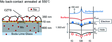
The effects of Na on Cu2ZnSnS4 (CZTS)-based solar cells have been examined with respect to surface potential and carrier transport. The Mo back-contact was annealed in a furnace for 10 minutes under a nitrogen atmosphere at different temperatures and CZTS thin films were subsequently grown by sputtering and sulfurization. The thickness of MoS2, formed during the sulfurization process, decreased as the Mo annealing temperature increased. Interestingly, the Na contents diffused from soda lime glass has increased as well. The current and surface potential near CZTS grain boundaries were investigated by Kelvin probe force microscopy (KPFM) and conductive atomic force microscopy (C-AFM) were used. Surface current increased with increasing annealing temperature and surface potential increased up to approximately 50 mV near GBs, which led to inhibition of electron–hole recombination and an increase in minority carrier collection near GBs. This observation explains the improvement of solar cell open circuit voltage (VOC) and current density (JSC).


1. Introduction

Owing to its low cost and high power conversion efficiency (PCE), Cu2ZnSnS4 (CZTS) is considered a promising material for thin film solar cells. Its useful band-gap energy (Eg) of 1.4–1.5 eV additionally makes it an attractive material for use in solar cells.1–8 When compared with Cu(In,Ga)Se2 (CIGS) thin film devices, those made of CZTS show rapid progress in performance.9,10 The highest PCE of Cu2ZnSn(S,Se)4 (CZTSSe) thin film solar cells, however, is 12.6%[thin space (1/6-em)]11 while that of CIGS is 22.3%.12 To fabricate high efficiency CZTS-based thin film solar cells, it is critically important to control the formation of secondary phases like CuS and ZnS.13–18 Moreover, interfacial layers such as MoS2 are additionally important in passivating grain boundaries (GBs) and reduce electron–hole pair recombination. To reduce the formation of MoS2, Yang et al.19 used a Mo annealing process with three different annealing temperatures (180, 370, and 550 °C). During the Mo annealing process, Na from the soda lime glass (SLG) substrate diffuses into CZTS GBs during the primary CZTS deposition stage. Shin et al. also demonstrated that the thickness of MoSe2 can be controlled by managing the Se partial pressure or by using a TiN diffusion barrier.20

Much is known about the role of Na on CIGS thin films. Contreras et al.21 demonstrated that Na passivates precursor layers and increases conductivity. Additionally, work by Yan et al.22 suggests that Na acts as a shallow donor at GBs. Guo et al.23 also indicated that Na incorporation led to structural enhancement, which led to inhibition of electron–hole recombination. Rudmann et al.24,25 and Zhang et al.26 used different substrate temperatures to induce Na diffusion and suggested that Na has a positive effect on grain size and device performance.

Although the effect of Na on CZTS solar cells is less well understood compared with CIGS solar cells, many groups have nonetheless suggested ways in which Na affects CZTS. Oo et al.27 revealed that the presence of Na enlarges the grain size of the CZTS solar cells. Prabhakar et al.28 compared CZTS precursors deposited on SLG and on Na-free glass substrates and suggested positive effects of Na. Gershon et al.29 have shown that Na increases grain size and passivates GBs, leading to a reduction in electron–hole pair recombination. Moreover, Lin et al.30 reported that Na incorporation increased carrier mobility thereby reducing electron–hole recombination and increasing current density. It has also been shown that Na diffusion decreased the thickness of the MoS2 layer and enhanced solar cell figures of merit such as open circuit voltage (VOC), fill factor (FF) and short circuit current density (JSC).19 When the thickness of the secondary phases decreased and the interfacial layers were controlled, CZTS solar cells exhibited increased PCE owing to increases in the figures of merit mentioned above.20,31

The role of Na on CZTSe has also been investigated. Li et al.32 prepared co-evaporated CZTSe on which Na increased the hole density and the built-in-potential of the junction, which resulted in an improvement in the VOC and FF of the solar cells. For mixed sulfide/selenide films, CZTSSe, Sutter-Fella et al.33 revealed that Na incorporation results in similar behavior compared with either of the unmixed cases. Na enhanced the grain size and the electrical properties as well. Kim et al.34 investigated CZTSSe with NaF layers. These layers increased the surface potential, which inhibited recombination in the depletion layer. In thin films, Na has a positive effect by passivating GBs. In solar cells, however, too much Na can act as an impurity in the buffer layer, which consequently increases recombination.35

In solar cell devices, it is known that the performance of the absorber layer is critical for efficiency as the absorber layer converts light into electrical energy. Previous studies have verified that GBs can positively affect the efficiency of thin film solar cells.36–39 In CZTSSe cells, GBs can enhance minority carrier collection by acting as a current pathway that allows minority carriers to reach the CdS buffer and ZnO layers.39 Furthermore, some studies have indicated that Na and O passivate GBs in CIGS thin films.40–42 The interfacial composition of CZTS, including secondary phases, can also affect its electrical properties. In particular, their thickness is inversely proportional to JSC.19,20,43 The VOC and the band alignment are additionally influenced by the interfacial composition.20,44,45

To develop a better mechanistic understanding of CZTS electrical properties, we investigated electrical current and potential on intra-grain (IG) surfaces and GBs with conductive atomic force microscopy (C-AFM) and Kelvin probe force microscopy (KPFM) measurements. Secondary ion mass spectrometry (SIMS), X-ray photoelectron spectroscopy (XPS), and Raman scattering spectroscopy are also used to investigate the CZTS films.

2. Experimental

The Mo back-contact layer was deposited on SLG with DC magnetron sputtering with a thickness of ∼600 nm. The Mo target had a purity of 99.99%, and three samples were annealed at 180, 370, and 550 °C for 10 minutes each in an N2 atmosphere at atmospheric pressure. For the deposition of the CZTS absorber layers, we employed 99.99% pure Cu (150 W DC power), SnS (200 W RF power), and ZnS (200 W RF power) with the stacking order of Cu/SnS/ZnS/Mo by sputtering method. These thin films were sulfurized together at atmospheric pressure with nitrogen atmosphere at 570 °C for 30 min.19 To investigate the electrical properties of the precursor surfaces and their GBs, a commercial atomic force microscope (AFM) (Nanofocus Inc., n-Tracer) was used. We used a Pt/Ir-coated tip (Nanosensor, PPP-EFM) for C-AFM and KPFM measurements. For C-AFM, we applied a bias voltage to the sample surfaces ranging from 0.1 to 0.5 V in a 5 × 5 μm2 scanning area. The conducting probe was connected to ground and current was detected with a single terminal. Simultaneously, it is possible to obtain morphological images in a contact mode. With KPFM, the surface potential of the CZTS surfaces was obtained without contact. The natural frequency of the tip was 68 kHz, the scan rate of the KPFM was less than 0.5 Hz, and the scan size was the same as that for the C-AFM measurement.46–52

3. Results and discussion

Statistical data of the device characteristics of the samples used in this study are given in Table 1 where the samples were annealed at three different temperate. According to previous research, the increase in VOC in CIGS thin film solar cells is due to trap energy levels becoming shallower.43 On the one hand, the shunt resistance (RSh) shows rather low in the 550 °C-annealed sample. This can be because of the changes in the Mo back-contact surface. As shown in Fig. S1, 550 °C-annealed Mo layer has the higher roughness, which can cause topographical defect near the interface. However, the improved absorber layer compensates the loss and perform better. The substrate temperatures are 180, 370, and 550 °C. We were able to see that as the Mo annealing temperature increases Na composition is also higher in Table 1 and Fig. S3. At the highest Mo annealing temperature, the MoS2 layer has the thinnest thickness. Herein, we will focus on the formation of MoS2 and the electrical properties incorporated by Na diffusion.
Table 1 Device parameters of the CZTS thin-film solar cells with and without annealing the Mo back-contact layers and Na component. RSe and RSh were obtain by IV curves in our previous report,19 where the composition of Na was determined by an inductively coupled plasma method
Mo annealing temperature [°C] η [%] FF [%] VOC [mV] JSC [mA cm−2] RSe [Ω cm2] RSh [Ω cm2] Na [%]
As-grown 1.49 ± 0.08 56.2 ± 2.55 494 ± 0.01 5.36 ± 0.23 0.44 457 1.84 ± 0.06
180 °C 1.32 ± 0.11 55.3 ± 2.37 473 ± 0.02 5.06 ± 0.11 1.05 520 2.08 ± 0.17
370 °C 2.23 ± 0.26 60.1 ± 4.89 535 ± 0.02 6.95 ± 0.35 1.17 593 2.87 ± 0.13
550 °C 4.07 ± 1.15 51.3 ± 17.32 576 ± 0.17 13.76 ± 3.48 0.77 295 3.13 ± 0.05


Fig. 1(a)–(d) are 2-dimensional AFM topography images of the absorber surfaces for the various Mo annealing temperatures. Fig. 1(e)–(h) display current map images taken while applying an external bias of 0.5 V. In Fig. 1(e)–(h), more current is exhibited at higher annealing temperatures. We analyzed their line profiles in Fig. 2 to compare the current formation near the GBs and the IGs. As the sample bias becomes larger and the Mo annealing temperature becomes higher, we find more and larger current is generated, particularly near the GBs. Additionally, Fig. S4 shows the IV curves of the samples, showing that the conductivity near the GBs are higher. This is because the surface current starts to flow near the GBs with the smaller external bias. Topography-surface current line profiles displayed in Fig. 2 reveal the current increased as the bias voltage is bigger, which corresponds to the IV curves. In Fig. 3(a), we compared VOC and JSC as a function of the Mo annealing temperature. From the Mo annealing temperature of 370 °C, VOC and JSC increased sharply, so that we can expect higher PCE of the solar cells. Fig. 3(b) is a graph showing the relationship between the average current on local surfaces, the current ratio and the Mo annealing temperature. Seeing the average current and the current ratio are proportionally related to the Mo annealing temperature, it is expected that the conductivity of the absorber surface increases overall. Azulay et al.37 reported that near GBs negative band bending occurs and photo-generated electron–hole pairs are separated by chemical and electrical gradients. Moreover, downward band bending around GBs creates a positively charged surface potential near GBs, leading to the concentration of minority carriers. This phenomenon improves JSC.53 Locally, based on the line profiles in Fig. 2, we can see the relationship between current, the external bias, and the Mo annealing temperatures. We compared positive average current at the GBs and the IG regions in Fig. 3(c). More current is generated near the GBs compared to the IG regions. This means that current path is developed near the GBs. It is observable that surface current is made the place which does not seem as GBs. It can be thought that the current is developed near the GBs which is located inside the thin film. Moreover, we could recognize which carriers – major or minor – pass the GBs through surface potential measurement. Then, it is possible to comprehend the carrier transport on the absorber surface.


image file: c6ra22563b-f1.tif
Fig. 1 (a)–(d) AFM topography images of the absorber surfaces for the various Mo annealing temperatures or the as-grown sample. (e)–(h) Current map images from C-AFM measurements with an external bias 0.5 V.

image file: c6ra22563b-f2.tif
Fig. 2 (a)–(d) Line profiles of current depending on grain boundaries (GBs) as a function of the Mo annealing temperature. As the sample bias voltage is higher, larger current is exhibited near the GBs.

image file: c6ra22563b-f3.tif
Fig. 3 (a) Comparison between open circuit voltage (VOC), current density (JSC) and Mo annealing temperature. (b) The proportional relation of average current and current ratio with the Mo annealing temperature. (c) Comparison of average current near the GBs.

KPFM results further confirm the presented C-AFM data. Fig. 4 shows topography, KPFM and their line profiles of IG regions and GBs. Fig. 4(a)–(d) are the topography images of the absorber layers. Fig. 4(e)–(h) are the surface potential mapping images from KPFM measurements. Topography-surface potential line profiles along GBs and IG regions are shown in Fig. 5(a)–(d). Near GBs, the positive surface potential tends to be larger. On the IG regions, however, a negative surface potential is likely to be formed. With the surface potential maps, we could see that positive potential is formed near the GBs. With the line profiles, we can more clearly determine the potential as a function of spatial location on the film, i.e. for GBs vs. IG regions. Fig. 6 shows the potential histograms for the IG regions and GBs. While Fig. 6(a)–(d) display the potential histograms in the IG regions as a function of Mo annealing temperature, Fig. 6(e)–(h) indicate that near the GBs, a more positively charged potential is observed. From the potential maps, we can extract the potential value near the GBs and the IGs over 50 points respectively and produce potential histograms for both regions. As the Mo annealing temperature is higher, with more Na diffusion, GBs would have more negative band bending and therefore more positive surface potential. This is because Na became distributed along GBs and passivates them. By reducing the electron–hole pair recombination, VOC will increase as the electron concentration is higher near the GBs, which ultimately increases solar cell PCE.50


image file: c6ra22563b-f4.tif
Fig. 4 Topography, surface potential maps and line profiles in IGs and GBs. (a)–(d) Topography images of the absorber layers. (e)–(h) Surface potential mapping images by KPFM measurements.

image file: c6ra22563b-f5.tif
Fig. 5 (a)–(d) Line profiles from the KPFM measurement both near the GBs and on the IGs. Near the GBs, the positive surface potential tends to be increased. On the IGs, however, negative surface potential is likely to be formed as the Mo annealing temperature is higher.

image file: c6ra22563b-f6.tif
Fig. 6 Potential histograms in IGs and GBs. (a)–(d) Potential histograms in the IGs for the various Mo annealing temperatures. (e)–(h) Potential histograms near the GBs, more positively charged potential tends to develop.

Annealed and unannealed Mo layers were sulfurized together to the Mo–S reaction level.19 Fig. 7 shows SIMS data of the as-grown and the annealed Mo and MoS2 layers. We believe that the differences in the surface morphology and grain size can be attributed to the difference in the heat transfer path and/or the diffusion of Na into the Mo layer from the SLG substrate during the annealing process. Consequently, gone through the sulfurization, the absorber layer can be affected by the diffused Na. SIMS depth profiles were therefore obtained to investigate the effects of Na diffusion from the Mo/SLG substrate into the MoS2 layers. Also, we can obtain that the Na is diffused into the CZTS thin films by XPS measurement (Fig. S3(c)). As shown in Fig. 7(a), the Na, O and S concentrations are rather constant with respect to film depth. After annealing the samples at 180 and 370 °C (Fig. 7(b) and (c)), the O and Na concentrations are slightly increased. At an annealing temperature of 550 °C (Fig. 7(d)), the Na and S concentration increases more noticeably in the MoS2 layer. These results indicate that some of the S evaporated at high temperature remained at the surface of the MoS2 layers during the cooling process. As shown in the SIMS profile results, the Na concentration in the MoS2 layer of the samples annealed at 180 and 370 °C increased slightly to around 2 × 10⁶ cps (Fig. 7(b) and (c)) compared with that of the as-grown sample (Fig. 7(a)), whereas that of the sample annealed at 550 °C (Fig. 7(d)) was over 107 cps. The addition of Na during the CZTS and CIGS deposition is known to increase grain size, free carrier concentration, and electrical conductivity.29,54 In this research, Mo coated SLG was annealed, and we could check Na contents were diffused upper layers like Mo/MoS2. As you can see in the SIMS depth profiles (Fig. S2), the highest annealing temperature of 550 °C make the Na diffused most. From this result, the Na is expected to have most effect on the sample annealed at 550 °C during the CZTS deposition and the post-sulfurization process. This is because its MoS2 layer surface could have more Na then any samples and the Na contents will be moved into the absorber layers. According to the previous report, the higher the annealing temperature was, the more the Na was diffused into ZnS.19 The effects of the incorporation of Na on the electrical properties of CZTS are similar to the case of CIGS, with an increase in the free carrier concentration due to a lower number of compensating donors.23–25,28 The addition of Na is also known to enhance cell performance by improving the VOC, FF, JSC, and thus PCE of the cells. Thus, we can say that the Mo annealing process before the deposition of the absorber plays a significant role in growth of CZTS thin-film solar cells. The Na dose, however, must be optimized because excessive or insufficient doping produces a detrimental effect on the cell performance. The incorporation of too much Na results in small grain sizes and porous films.55 The poor structural properties of the front-annealed CZTSe thin film were therefore likely caused by the relatively large amount of Na diffused from the Mo/SLG substrate which led to the degradation of the film's electrical properties.


image file: c6ra22563b-f7.tif
Fig. 7 SIMS composition profiles of annealed Mo back contact layers after sulfurization process. Each component shows its intensity differences in Mo and MoS2 layers depending on the Mo annealing temperatures. The Na concentration of the sample annealed at 550 °C increased sharply.

Fig. 8 shows the schematic images of Na diffusion and a band bending diagram of the samples without and with Na. Fig. 8(a) and (b) show Na have benign effect on the CZTS precursor layer if the Mo annealing temperature is higher. Fig. 8(a) has less Na in the absorber layer and the thickness of MoS2 is greater. The Mo annealing process, however, encourages the Na to diffuse into the CZTS layers and little MoS2 is formed. Previously we reported that Mo annealed samples have less MoS2. This is because oxygen deactivates the reaction between S and Mo.19 Though we cannot directly determine the relation between the thickness of the MoS2 and the electrical properties from the data presented here, we propose that less MoS2 leads to the enhancement of the solar cell performance as observed in previous research. MoS2 is formed by sulfurization. As excessive MoS2 has a negative influence on the energy band-gap because it can make a band gap barrier between Mo back contact layer and the absorber layer. If the barrier is too high or too sharp, carrier transport would be interrupted and deteriorate electrical properties of the solar cells. That is why controlling its formation is important to prevent reaction with Zn and Sn.56,57 From the results of the C-AFM and KPFM measurements, we can derive the schemas of band bending near GBs, as shown in Fig. 8(c) and (d). Since the Mo annealing temperature is higher, surface potential is increased to ∼50 mV while the as-grown sample exhibits a surface potential of ∼10 mV. This indicates that Na diffused along GBs, thus passivating them. As Na is always positively charged, higher and positively charged potential is observed near GBs, which leads to downward band bending. This band bending will repel the majority carriers from the GBs.22 Simultaneously, a stronger electric field is created at the GBs, which draws minority carriers toward the GBs and improves JSC.58 This stronger electric field can increase the concentration of electrons near the GBs. Under these conditions, electron–hole pair recombination is suppressed. The GBs will then act as the dominant current path, which is governed by the minority carriers. This behavior leads to the improvement of solar cell figures of merit like VOC and JSC and thus PCE. These results are in agreement with previous research that has investigated the role of CZTS GBs.39,52


image file: c6ra22563b-f8.tif
Fig. 8 Schematic images of Na diffusion and suppression of the thickness of MoS2 layers. (a) and (b) Show the difference in Na content between the as-grown sample and the 550 °C annealed sample. (c) and (d) Show the corresponding band bending near GBs with and without Na on the surface.

4. Conclusions

We verified that solar cell performance improves with a Mo annealing process. We investigated the electrical and compositional properties of the absorber surfaces with C-AFM, KPFM and SIMS measurement. At higher Mo annealing temperatures, the current at the absorber surface is increased, and the surface potential is improved near GBs. Positive surface potential develops near GBs whereas it is negative in IG regions. From SIMS measurements, we determined that more Na is diffused Mo layer and passivate the GBs into the CZTS absorber layers at the highest annealing temperature (550 °C). In particular, Na that diffuses enough into the Mo/MoS2 can lead to the suppression of MoS2 and is expected to be diffused into the CZTS absorber layer during the precursor deposition and post-sulfurization process. This could improve hole transport across the CZTS/Mo interface to the Mo layer. Additionally, as the electron–hole pair recombination is reduced, JSC increases, causing the solar cell performance to improve. The Mo annealing process thus improves device performance and enhances the electrical properties of CZTS thin film solar cells.

Acknowledgements

This work was supported by the New & Renewable Energy of the Korea Institute of Energy Technology Evaluation and Planning (KETEP) grant funded by the Korea government, Ministry of Trade, Industry, and Energy. (No. 20123010010130).

References

  1. K. Ito and T. Nakazawa, Jpn. J. Appl. Phys., 1988, 27, 2094 CrossRef CAS.
  2. H. Katagiri, K. Jimbo, S. Yamada, T. Kamimura, W. S. Maw, T. Fukano, T. Ito and T. Motohiro, Appl. Phys. Express, 2008, 1, 041201 CrossRef.
  3. K. Ramasamy, M. A. Malik and P. O'Brien, Chem. Commun., 2012, 48, 5703 RSC.
  4. J. J. Scragg, P. J. Dale and L. M. Peter, Thin Solid Films, 2009, 517, 2481 CrossRef CAS.
  5. H. Katagiri, K. Saitoh, T. Washio, H. Shinohara, T. Kurumadani and S. Miyajima, Sol. Energ. Mat. Sol. Cells, 2001, 65, 141 CrossRef CAS.
  6. H. Katagiri, K. Jimbo, W. S. Maw, K. Oishi, M. Yamazaki, H. Araki and A. Takeuchi, Thin Solid Films, 2009, 517, 2455 CrossRef CAS.
  7. N. Yu, R. Zhong, W. Zhong, X. Chen, J. Luo, X. Gu, X. Hu, L. Zhang, J. Hu and Z. Chen, RSC Adv., 2014, 68, 36046 RSC.
  8. L. Yin, G. Cheng, Y. Feng, Z. Li, C. Yang and X. Xiao, RSC Adv., 2015, 5, 4069 RSC.
  9. S. Chen, X. G. Gong, A. Walsh and S.-H. Wei, Phys. Rev. B, 2009, 79, 165211 CrossRef.
  10. P. Jackson, D. Hariskos, E. Lotter, S. Paetel, R. Wuerz, R. Menner, W. Wischmann and M. Powalla, Prog. Photovolt: Res. Appl., 2011, 19, 894 CrossRef CAS.
  11. W. Wang, M. T. Winkler, O. Gunawan, T. Gokmen, T. K. Todorov, Y. Zhu and D. B. Mitzi, Adv. Energy Mater., 2014, 4, 1301465 CrossRef.
  12. J. Gifford, Solar Frontier Hits 22.3% on CIGS Cell. Industry and Suppliers, Market and Trends, 2015, http://www.solar-frontier.com/eng/news/2015/C051171.html.
  13. G. S. Babu, Y. B. K. Kumar, P. U. Bhaskar and S. R. Vanjari, Sol. Energ. Mat. Sol. Cells, 2010, 94, 221 CrossRef.
  14. H. Yoo and J. H. Kim, Thin Solid Films, 2010, 518, 6567 CrossRef CAS.
  15. O. Vigil-Galán, M. Espíndola-Rodríguez, M. Courel, X. Fontané, D. Sylla, V. Izquierdo-Roca, A. Fairbrother, E. Saucedo and A. Pérez-Rodríguez, Sol. Energ. Mat. Sol. Cells, 2013, 117, 246 CrossRef.
  16. X. Fontané, L. Calvo-Barrio, V. Izquierdo-Roca, E. Saucedo, A. Pérez-Rodriguez, J. R. Morante, D. M. Berg, P. J. Dale and S. Siebentritt, Appl. Phys. Lett., 2011, 98, 181905 CrossRef.
  17. T. Schnabel, M. Löw and E. Ahlswede, Sol. Energ. Mat. Sol. Cells, 2013, 117, 324 CrossRef CAS.
  18. Y. E. Romanyuk, C. M. Fella, A. R. Uhl, M. Werner, A. N. Tiwari, T. Schnabel and E. Ahlswede, Sol. Energ. Mat. Sol. Cells, 2013, 119, 181 CrossRef CAS.
  19. K.-J. Yang, J.-H. Sim, B. Jeon, D.-H. Son, D.-H. Kim, S.-J. Sung, D.-K. Hwang, S. Song, D. B. Khadka, J. H. Kim and J.-K. Kang, Prog. Photovolt: Res. Appl., 2015, 23, 862 CrossRef CAS.
  20. B. Shin, Y. Zhu, N. A. Bojarczuk, S. J. Chey and S. Guha, Appl. Phys. Lett., 2012, 101, 053903 CrossRef.
  21. M. A. Contreras, B. Egaas, P. Dippo, J. Webb, J. Granata, K. Ramanathan, S. Asher, A. Swartzlander and R. Noufi, Photovoltaic Specialists Conference, Conference Record of the Twenty-Sixth IEEE, 1997, p. 359 Search PubMed.
  22. Y. Yan, C.-S. Jiang, R. Noufi, S.-H. Wei, H. R. Moutinho and M. M. Al-Jassim, Phys. Rev. Lett., 2007, 99, 235504 CrossRef PubMed.
  23. Q. Guo, G. M. Ford, R. Agrawal and H. W. Hillhouse, Prog. Photovolt: Res. Appl., 2013, 21, 64 CrossRef CAS.
  24. D. Rudmann, A. F. da Cunha, M. Kaelin, F. Kurdesau, H. Zogg, A. N. Tiwari and G. Bilger, Appl. Phys. Lett., 2004, 84, 1129 CrossRef CAS.
  25. D. Rudmann, D. Brémaud, A. F. da Cunha, G. Bilger, A. Strohm, M. Kaelin, H. Zogg and A. N. Tiwari, Thin Solid Films, 2005, 480–481, 55 CrossRef CAS.
  26. L. Zhang, Q. He, W.-L. Jiang, F.-F. Liu, C.-J. Li and Y. Sun, Sol. Energ. Mat. Sol. Cells, 2009, 93, 114 CrossRef CAS.
  27. W. M. H. Oo, J. L. Johnson, A. Bhatia, E. A. Lund, M. M. Nowell and M. A. Scarpulla, J. Electron. Mater., 2011, 40, 2214 CrossRef.
  28. T. Prabhakar and N. Jampana, Sol. Energ. Mat. Sol. Cells, 2011, 95, 1001 CrossRef CAS.
  29. T. Gershon, B. Shin, N. Bojarczuk, M. Hopstaken, D. B. Mitzi and S. Guha, Adv. Energy Mater., 2015, 5, 1400849 CrossRef.
  30. Y.-R. Lin, V. Tunuguntla, S.-Y. Wei, W.-C. Chen, D. Wong, C.-H. Lai, L.-K. Liu, L.-C. Chen and K.-H. Chen, Nano Energy, 2015, 16, 438 CrossRef CAS.
  31. K.-J. Yang, J.-H. Sim, D.-H. Son, D.-H. Kim, G. Y. Kim, W. Jo, S. Song, J. H. Kim, D. Nam, H. Cheong and J.-K. Kang, Prog. Photovolt: Res. Appl., 2015, 23, 1771 CrossRef CAS.
  32. J. V. Li, D. Kuciauskas, M. R. Young and I. L. Repins, Appl. Phys. Lett., 2013, 102, 163905 CrossRef.
  33. C. M. Sutter-Fella, J. A. Stückelberger, H. Hagendorfer, F. La Mattina, L. Kranz, S. Nishiwaki, A. R. Uhl, Y. E. Romanyuk and A. N. Tiwari, Chem. Mater., 2014, 26, 1420 CrossRef CAS.
  34. G. Y. Kim, J. Kim, W. Jo, D.-H. Son, D.-H. Kim and J.-K. Kang, Nano Convergence, 2014, 1, 1 CrossRef.
  35. K.-J. Yang, J.-H. Sim, D.-H. Son, D.-H. Kim and J.-K. Kang, Curr. Appl. Phys., 2015, 15, 1512 CrossRef.
  36. C.-S. Jiang, R. Noufi, K. Ramanathan, J. A. AbuShama, H. R. Moutinho and M. M. Al-Jassim, Appl. Phys. Lett., 2004, 85, 2625 CrossRef CAS.
  37. D. Azulay, O. Millo, I. Balberg, H.-W. Schock, I. Visoly-Fisher and D. Cahen, Sol. Energ. Mat. Sol. Cells, 2007, 91, 85 CrossRef CAS.
  38. I. Visoly-Fisher, S. R. Cohen, A. Ruzin and D. Cahen, Adv. Mater., 2004, 16, 879 CrossRef CAS.
  39. J. B. Li, V. Chawla and B. M. Clemens, Adv. Mater., 2012, 24, 720 CrossRef CAS PubMed.
  40. L. Kronik, D. Cahen and H. W. Schock, Adv. Mater., 1998, 10, 31 CrossRef CAS.
  41. L. Kronik, U. Rau, J.-F. Guillemoles, D. Braunger, H.-W. Schock and D. Cahen, Thin Solid Films, 2000, 361–362, 353 CrossRef CAS.
  42. D. Cahen and R. Noufi, Appl. Phys. Lett., 1989, 54, 558 CrossRef CAS.
  43. X. Zhu, Z. Zhou, Y. Wang, L. Zhang, A. Li and F. Huang, Sol. Energ. Mat. Sol. Cells, 2012, 101, 57 CrossRef CAS.
  44. O. Gunawan, T. K. Todorov and D. B. Mitzi, Appl. Phys. Lett., 2012, 97, 233506 CrossRef.
  45. B. Shin, N. A. Bojarczuk and S. Guha, Appl. Phys. Lett., 2013, 102, 091907 CrossRef.
  46. G. Y. Kim, W. Jo, K. D. Lee, H.-S. Choi, J. Y. Kim, H.-Y. Shin, T. T. T. Nguyen, S. Yoon, B. S. Joo, M. Gu and M. Han, Sol. Energ. Mat. Sol. Cells, 2015, 139, 10 CrossRef CAS.
  47. G. Y. Kim, D.-H. Son, T. T. T. Nguyen, S. Yoon, M. Kwon, C.-W. Jeon, D.-H. Kim, J.-K. Kang and W. Jo, Prog. Photovolt: Res. Appl., 2016, 24, 292 CrossRef CAS.
  48. A. R. Jeong, G. Y. Kim, W. Jo, D. Nam, H. Cheong, H. J. Jo, D.-H. Kim, S.-J. Sung, J.-K. Kang and D. H. Lee, Adv. Nat. Sci.: Nanosci. Nanotechnol., 2013, 4, 015007 CrossRef.
  49. R. H. Shin, A. R. Jeong and W. Jo, Curr. Appl. Phys., 2012, 12, 1313 CrossRef.
  50. G. Y. Kim, J. R. Kim, W. Jo, D.-H. Son, D.-H. Kim and J.-K. Kang, Nanoscale Res. Lett., 2014, 9, 10 CrossRef PubMed.
  51. A. R. Jeong, W. Jo, S. Jung, J. Gwak and J. H. Yun, Appl. Phys. Lett., 2011, 99, 082103 CrossRef.
  52. G. Y. Kim, J. R. Kim, W. Jo, K. D. Lee, J. Y. Kim, T. T. T. Nguyen and S. Yoon, Curr. Appl. Phys., 2014, 14, 1665 CrossRef.
  53. G. Y. Kim, A. R. Jeong, J. R. Kim, W. Jo, D.-H. Son, D.-H. Kim and J.-K. Kang, Sol. Energy Mater. Sol. Cells, 2014, 127, 129 CrossRef CAS.
  54. D. J. Schroeder and A. A. Rockett, J. Appl. Phys., 1997, 82, 4982 CrossRef CAS.
  55. D. Rudmann, Ph.D. thesis, Swiss Federal Institute of Technology, Zürich, Switzerland, 2004.
  56. R. S. Sundaram, M. Engel, A. Lombardo, R. Krupke, A. C. Ferrari, P. Avouris and M. Steiner, Nano Lett., 2013, 13, 1416 CrossRef CAS PubMed.
  57. K. K. Kam and B. A. Parkinson, J. Phys. Chem., 1982, 86, 463 CrossRef CAS.
  58. M. Gloeckler, J. R. Sites and W. K. Metzger, J. Appl. Phys., 2005, 98, 113704 CrossRef.

Footnote

Electronic supplementary information (ESI) available. See DOI: 10.1039/c6ra22563b

This journal is © The Royal Society of Chemistry 2016
Click here to see how this site uses Cookies. View our privacy policy here.