Extraordinary magneto-optical Kerr effect via MoS2 monolayer in Au/Py/MoS2 plasmonic cavity

A. H. Baradaran Ghasemi*a, E. Faridia, N. Ansarib and S. M. Mohsenia
aDepartment of Physics, Shahid Beheshti University, G.C. Evin, Tehran 19839, Iran. E-mail: a_b.ghasemi@sbu.ac.ir
bDepartment of Physics, Alzahra University, Tehran 19938, Iran

Received 24th August 2016 , Accepted 22nd October 2016

First published on 24th October 2016


Abstract

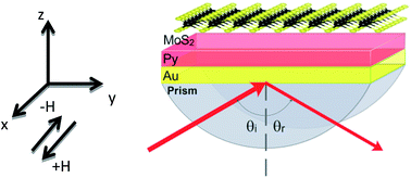
We demonstrate a multilayer magnetoplasmonic structure fabricated from MoS2 monolayer to significantly increase the magneto-optical Kerr effect (MOKE). The structure is made from glass/Au/Py/MoS2 × n (where n is the number of MoS2 monolayers), and the MOKE enhancements are based on the surface plasmon resonance and the extraordinary light absorbing mechanism of the MoS2 monolayers. The transverse MOKE (TMOKE) is about 18 times larger than that of Au/Py, suggesting the important role of the MoS2 top layer. Moreover, the calculated Q-factor of the TMOKE signal is found to be about 623, indicating the presence of a sharp cavity resonance that dramatically influences the surface plasmon excitation. Our results convey a new pathway to the design of advanced magneto-optical devices for sensors, recording, etc.


1. Introduction

The magneto-optical Kerr effect (MOKE) is one of the promising characteristics for the design of advanced nano-optical devices.1–3 This effect shows small signal to noise amplitude, particularly in thin film structures, and alternative techniques exist to improve the performances in this area. The transverse MOKE (TMOKE), in contrast to the longitudinal MOKE (LMOKE), can be significantly enhanced through structural design for application in magneto-optical recording elements,4–6 sensors7–9 and integrated photonic isolators.10,11 TMOKE is a magneto-optical (MO) effect in which reflected intensity from the MO medium is sensitive to alteration in the external magnetic field due to coupling of the transverse elliptical-polarized optical field with electrons in the MO medium.12 It is also polarization invariant and only occurs for TM-polarized light when the electric field vector of the incident light is parallel to the plane of incidence. However, the MO activity in conventional TMOKE structures consisting of ferromagnetic thin films needs to be strong enough in order to be useful for the underlying applications.13,14

Several techniques have been proposed to enhance the MO activity of composite structures.15–17 One successful idea for enhancing TMOKE is to excite surface plasmon polariton (SPP) modes in metal–dielectric structures.18–20 SPPs are electromagnetic modes that can be excited through coupling of transverse electromagnetic waves to the free electrons in metals where they are localized in between the interface of the metal–dielectric stack. The key idea in making use of SPP excitation for strong TMOKE response is that a field component of the SPP mode that is perpendicular to the metal surface is evanescent, leading to excitation of transverse elliptical polarized-optical waves at the metal–dielectric interface.21 Furthermore, combining TMOKE with SPP results in miniaturization of the device structure.

Recent experimental and theoretical investigations regarding structures composed of conducting ferromagnetic and noble-metal layers like Au/Co/Au,22,23 as well as periodic metal–dielectric heterostructures consisting of noble metallic grating deposited on dielectric magnetic layers (magnetoplasmonic crystals),24,25 show a strong increase of TMOKE magnitude, which is observed at weak external magnetic field through SPP excitation. Accordingly, substantial effort has been devoted to the proposal of a magnetoplasmonic structure with stronger TMOKE through an enhancement of the surface plasmon resonance (SPR) and MO activity.

One of the main effective physical parameters in magnetoplasmonics is the carrier concentration in the structure. This parameter can directly affect the optical loss, the strength of excited SPP and the MO activity in the stack. An increase in carrier concentration and optical absorption in the magnetic material results in the excitation of further electrons for interactions that are responsible for TMOKE.21 On the other hand, the existence of an electronic bandgap in the desired frequency spectrum can control the interband transition, which is responsible for optical losses in the materials. Accordingly, selection of a material with a bandgap that is larger than the desired frequency spectrum leads to mitigation of the overall loss for the device. Therefore, one effective method for TMOKE enhancement is to make use of materials with definite carrier concentrations and electronic band gaps in the structural design of the nano-optical device.26

Recently, there has been much interest in a certain type of layered transition-metal dichalcogenide (TMDC)27–29 semiconductor groups, such as molybdenum disulfide (MoS2), due to their novel electronic and optical properties, which open up new opportunities for optoelectronic applications.30–35 Specifically, MoS2 monolayer has a direct band gap of 1.9 eV (ref. 36) (near the photon energy of He–Ne lasers) due to quantum confinement effects with high absorption efficiency and very high charge mobility that makes it a good candidate for exciting further electrons in the TMOKE structures. Furthermore, several experimental techniques have been employed to synthesize MoS2 monolayer.9,37 There are some advanced methods for the growth of single-crystal monolayer MoS2 that use chemical vapor deposition (CVD) method,38 or room temperature ionic liquids (RTIL) as an electrolyte for the electrodeposition of MoS2 thin films.39 Based on these properties, a recent study on a hybrid plasmonic structure composed of graphene–MoS2 layers demonstrated ultrasensitive detection of molecules.40

In this study, we make a theoretical demonstration of a multilayer structure that promises giant enhancement in TMOKE response. The structure consists of MoS2 monolayers/permalloy (9 nm)/Au (9 nm)/glass, where the numbers are the thicknesses in nm and permalloy (Py) is a well-known NiFe alloy. We vary the number of MoS2 monolayers and study the details of wavelength and angle dependent reflectivity and TMOKE response in the stack. The TMOKE response is found to be at least one order of magnitude larger than that of conventional TMOKE structures. Moreover, the calculated Q-factor of the TMOKE signal is about 623, which means that a sharp cavity resonance occurs at the SPP excitation wavelength. The structure design parameters for the signal optimization are the number of MoS2 layers and the thickness of the Py nanolayer in the stack. Firstly, having fixed the Au thickness, the TMOKE signal was optimized through Py thickness and incident light angle variations in a stack without the MoS2 layer. Secondly, having fixed the optimized value of Py thickness, we investigated the effect of MoS2 layers on TMOKE response. The theoretical method for calculating TMOKE is described in Section 2. The proposed structure and the respective parameters are explained in Section 3. Section 4 is devoted to results and discussion. The last section concludes with the main points of this study.

2. Theory

The theoretical framework, which is used in this study, is based on the transfer matrix method (TMM) for dispersive and anisotropic structures. The mathematical models, which have been considered in this study for evaluating the material optical response, the physical condition through which SPR is excited in the proposed structure and the appropriate physical parameters for calculation of TMOKE, are explained in the following subsections.

2.1 Tensor nature of material optical response

We will first obtain the relative permittivity tensor of magnetic material based on the Drude–Lorentz model in the presence of a magnetic field. When the magnetic field is applied, the induced magnetization causes the different components to couple to each other. Accordingly, the optical response of the material can be evaluated through a non-diagonal permittivity tensor. When the external magnetic field is aligned to be in the plane of the sample and perpendicular to the incident plane, the so-called transverse configuration, the resulting permittivity tensor can read as follows:41
 
image file: c6ra21314f-t1.tif(1)
where image file: c6ra21314f-t2.tif is the MO constant, ε is the dielectric function of the non-magnetized film, and M is magnetization of the magnetic film. Non-diagonal elements depend on the orientation of magnetization, and ε1(−M) = −ε1(M).

The motion of the electron in the presence of a magnetic field can be investigated according to the following equation:42

 
image file: c6ra21314f-t3.tif(2)
where m, [r with combining right harpoon above (vector)], γ, [E with combining right harpoon above (vector)] and [B with combining right harpoon above (vector)]0 are the electron effective mass, the electron's position vector, damping constant, electric field vector of the incident wave and the applied magnetic field, respectively. ω0 is the band electron resonance frequency. We consider the external magnetic field to be in the direction of the x-axis;
 
[B with combining right harpoon above (vector)] = B0[x with combining circumflex]. (3)

In phasor notation, the position vector and electric field vector are considered according to the following equations:

 
[r with combining right harpoon above (vector)] = [r with combining right harpoon above (vector)]0[thin space (1/6-em)]e−iωt, (4)
 
[E with combining right harpoon above (vector)] = [E with combining right harpoon above (vector)]0[thin space (1/6-em)]e−iωt. (5)

Inserting eqn (3)–(5) into eqn (2), one can find [r with combining right harpoon above (vector)] in terms of [E with combining right harpoon above (vector)]. The conduction tensor image file: c6ra21314f-t4.tif is defined according to the following relationship:

 
image file: c6ra21314f-t5.tif(6)
whereN0, [v with combining right harpoon above (vector)] and [j with combining right harpoon above (vector)] are the electron density, velocity and current density, respectively. The relationship between the dielectric tensor image file: c6ra21314f-t6.tif and conducting tensor image file: c6ra21314f-t7.tif is given as follows:
 
image file: c6ra21314f-t8.tif(7)
where I is unitary matrix. By inserting eqn (7) into eqn (6), one can obtain ε and ε1 as follows:
 
image file: c6ra21314f-t9.tif(8)
 
image file: c6ra21314f-t10.tif(9)

We make use of eqn (8) and (9) for extracting the results illustrated in Fig. 6.

2.2 SPR excitation

With increasing the incident angle at boundaries between media having indices with opposite sign, the vertical wave vector component will be purely imaginary at a critical incident angle. The optical wave does not propagate in vertical directions, but decays exponentially with distance from the interface due to coupling with surface plasmon. Therefore, light propagates between the boundaries of media resulting in enhancement of the electric field in that region. For the simplest case, when SPP wave propagates between metal and dielectric medium, the dispersion relationship of SPP can be derived from the well-known Maxwell's equation under the following boundary condition:43
 
image file: c6ra21314f-t11.tif(10)
where εd and εm(ω) are the permittivity of the dielectric medium and metal, respectively. Also, Re denotes the real part of the complex function. Since the SPP wave vector kspp is always larger than the optical wave vector in the dielectric medium k(ω) over the entire spectrum, the SPPs cannot directly couple with the incoming light into the dielectric medium. Coupling between incoming light and SPP wave vector is obtained only when light travels in a medium with a refractive index larger than 1. Therefore, it happens under the following condition:
 
k(ω)sin(θ) = kspp(ω), (11)
where θ is the incident light angle.

Moreover, in the presence of an external magnetic field, time reversal symmetry is broken. Thus, the SPP wave vector is highly dependent on the direction of the magnetic field and exhibits nonreciprocal behavior: [k with combining right harpoon above (vector)](+H) ≠ [k with combining right harpoon above (vector)](−H). Such a magnetic field exerts an influence over the angular reflection curve according to [R with combining right harpoon above (vector)](+H) ≠ [R with combining right harpoon above (vector)](−H). The SPR excitation angle is shifted compared with that of a zero external magnetic field.

2.3 TMOKE calculation

We made use of TMM for one-dimensional multilayer structures to optimize the device for maximum MO activity. We assume that the incident light wave enters obliquely into the glass side of the proposed structure. Using boundary conditions for the tangential component of the electric and magnetic fields, we derive a relationship between electric field amplitudes in the boundary of the first and the last layers, which can be expressed as follows:41
 
image file: c6ra21314f-t12.tif(12)
where Ei and Ef are amplitudes of the electric fields at the bottom surface of the initial and final medium. D(n) is the medium boundary matrix, which depends to on the optical properties of the medium, and P(n) is the propagation matrix, which depends on the thickness of the layers. Accordingly, the Fresnel constant in terms of the scattering matrix can express as follows:
 
image file: c6ra21314f-t13.tif(13)

Rpp = |rpp|2,
where Rpp is the intensity of reflected TM-polarized light.

The transverse Kerr signal is recognized as a relative change in the TM-polarized light (p-polarization) intensity upon reversal of the external magnetic field when magnetization lies in the plane of the magnetic layer and perpendicular to the incident plane. In this configuration, polarization of light does not change. Accordingly, the TMOKE signal can be calculated through the relative change in reflected light intensity in opposite magnetization according to the following relationship:

 
image file: c6ra21314f-t14.tif(14)

R(H = 0) and R(+H) − R(−H) in eqn (14) are the pure optical and MO contributions of the transverse Kerr signal, respectively.

3. TMOKE structure

In this article, a glass/Au/Py/MoS2 multilayer was employed for the enhancement of MO-activity through excitation of SPP based on the Kretschmann configuration;43 it is illustrated in Fig. 1.
image file: c6ra21314f-f1.tif
Fig. 1 Schematic of a glass/Au/Py/MoS2 multilayer based on the Kretschmann configuration. External magnetic field (H) modulation has been shown through two opposite vectors along the x-axis.

The real and imaginary parts of the relative permittivity of the different layers are extracted in terms of optical frequencies by the relevant data included in the literature.44–46

The structure is located on a semi-cylindrical prism (BK7) and illuminated by a monochromatic He–Ne laser beam at 632.8 nm wavelength. According to Fig. 2, the complex dielectric constants of glass, Au, Py and MoS2 at 632.8 nm wavelength are εg = 2.2955, εAu = −10.2393 + 1.3694i, εpy = −7.1481 + 17.7165i,44 and εMoS2 = 15.7987 + 5.6536i,45 respectively. Moreover, the non-diagonal dielectric constant of the magnetic Py layer is considered to be ε1 = −0.0960 + 2023i.44


image file: c6ra21314f-f2.tif
Fig. 2 (a) Real and (b) imaginary parts of the dielectric constant of Au, Py and MoS2 versus wavelength.

4. Results and discussion

Based on our previous studies,6 we fixed the thickness of the Au layer at 9 nm and investigated the behavior of reflection and TMOKE intensity in terms of the incident angle and Py thickness to optimize the TMOKE response. Pure optical and MO contributions of the transverse Kerr and TMOKE signals versus Py thickness and incident angle have been shown in Fig. 3. As we can see in Fig. 3a, pure optical reflection R(H = 0) reaches its maximum value at 42.2°, corresponding to the critical angle, due to total internal reflection (TIR). The minimum value occurs at 48.65°, corresponding to SPR excitation for 9 nm Py thickness. In Fig. 3b, the MO component is plotted versus the incident angle and Py thickness.
image file: c6ra21314f-f3.tif
Fig. 3 (a) Pure optical reflection in glass/Au/Py multilayer versus incident angle and Py thickness; (b) MO reflection ΔR versus incident angle and Py thickness; (c) transfer Kerr signal versus incident angle and Py thickness. Pure optical reflection, MO reflection and transfer Kerr signal are shown through color density.

Since the magnetic layer is responsible for MO-activity, ΔR is vanishingly small for very thin layer of Py (about 0.5 nm in thickness) over the entire range of incident angles. With increasing the Py thickness, the MO activity rises appreciably and the pure MO part of the TMOKE signal is enhanced at 44.3°. However, optical absorption increases as Py thickness grows. According to Fig. 3c, the maximum value of the TMOKE signal eventually appears at 9 nm Py layer thickness and 48.65° incident angle. It should be noted that there is no MoS2 layer in the results extracted from Fig. 3. In the next step for evaluating the desired effect of MoS2 layers on boosting TMOKE signal, MoS2 layers are considered to be deposited on top of the previous structure, as shown in Fig. 1. The results are illustrated in Fig. 4.


image file: c6ra21314f-f4.tif
Fig. 4 (a) Reflection of TM-polarized light from glass/Au/Py/MoS2 × n versus incident angle, (b) TMOKE signal from glass/Au/Py/(MoS2)n versus incident angle, and (c) minimum reflection and maximum TMOKE versus the number of MoS2 layers.

According to Fig. 4a, the amount of reflected intensity around SPR excitation is reduced compared to the corresponding structure without the MoS2 layer. Moreover, according to Fig. 4b, the MoS2 layers lead to significant enhancement of the TMOKE signal.

When the number of MoS2 layers is increased, the total internal reflection angle (corresponding to maximum reflection) doesn't change, however the minimum reflected intensity shifts to a larger incident angle. This behavior can be explained in terms of the large value of the real part of the MoS2 refractive index, which results in SPR excitation at a larger angle according to eqn (11) for the wave vector matching condition at the material interface. Furthermore, because of a nonzero imaginary part of the dielectric constant of MoS2, the optical absorption of the layer increases leading to the broadening of the reflection curve. As the number of MoS2 layers is increased to more than 5 layers, the reflection curves become too wide to recognize the SPP reflection angle (Fig. 4a). Enhancement of TMOKE signal is highly dependent on the SPR excitation condition. According to Fig. 4b, the magnitude of the TMOKE signal increases drastically with decreasing the minimum reflected intensity. For a large incident angle away from SPR excitation, the magnitude of the signal decreases dramatically. The impact of the number of MoS2 layers on the minimum pure optical reflectivity and on the maximum value of the achieved TMOKE signal are illustrated in Fig. 4c. According to Fig. 4, the maximum value for the Kerr signal is achieved at 53.13° incident angle in the structure consisting of four layers of MoS2. Increasing the number of MoS2 layers to more than four results in a decrease in the TMOKE signal, which can be explained through the dissipation growth due to the imaginary part of the MoS2 dielectric constant.

MoS2 layers can alter the pure MO component ΔRH) by changing the magnetoplasmonic wave vector. We can see in Fig. 5 that when four layer of MoS2 are added on top of the structure, there is no appreciable change inΔRH) for incident angles smaller than the critical angle of 43.2°. In contrast, at incident angles larger than the critical angle, the pure MO component becomes very sensitive to any change in the layer on top of the structure. Because of the large refractive index of MoS2, the wave vector of SPP increases, leading to a shift in ΔRH). Eventually, the pure MO component shifts compared with the scheme related to the structure without the MoS2 layer. According to Fig. 4, at 53.13° and 48.65° incident angles, corresponding to SPR excitation angles for the structures with and without MoS2 layers, respectively, the change in ΔRH) is about −5.4 × 10⁻⁷. This analysis shows that the pure MO component of TMOKE decreases slightly in a structure comprised of MoS2 layers because of the imaginary part of the dielectric constant of MoS2, which results in energy dissipation. The calculated minimum values of R(H = 0), maximum values of TMOKE signals, and the enhancement factor at different number of MoS2 layers are tabulated in Table 1.


image file: c6ra21314f-f5.tif
Fig. 5 Pure MO component of the Kerr signal versus incident angle. The inset shows the difference between R(+H) − R(−H) in the multilayer structures with and without the MoS2 layer. The black dots in the inset shows the SPP incident angles in the two structures.
Table 1 The calculated TMOKE enhancement factors in terms of different numbers of MoS2 layers, accompanied by respective SPR excitation angle and pure optical reflection are summarized. The enhancement factors are normalized to that of a structure with no MoS2 layer
Number of MoS2 layers SPR excitation angle R(H = 0) TMOKE signal Enhancement factor
0 48.65° 0.0001894 0.24 1
1 49.58° 6.913 × 10⁻⁵ 0.55 1.68
2 50.63° 1.647 × 10⁻⁵ 0.87 3.61
3 51.82° 1.264 × 10⁻⁶ 4.00 16.59
4 53.13° 1.777 × 10⁻⁷ 4.40 18.48
5 54.57° 3.59 × 10⁻⁷ 3.70 15.32


In order to illustrate the surface plasmon excitation in the proposed structure, reflection in terms of both wavelength and incident angles have been shown in Fig. 6. The color density illustrates the reflection (R) according to the color bar in the figure. The dark blue color shows the SPP excitation, with a high reflection around 42°, which is illustrated with a yellow color, and corresponds to the critical angle due to the total internal reflection.


image file: c6ra21314f-f6.tif
Fig. 6 Reflection in the Au/Py/MoS2 (×4) multilayer versus wavelength and incident angles is illustrated through colors. The dark blue color shows the minimum reflection.

We employ TMM to study the EM field distribution and Poynting vector component along the surface inside the Au/Py/MoS2 (×4) multilayer at the SPP resonance angle at θ = 53.13°. When SPP is excited, the EM field increases gradually through the structure. Its maximum value takes place in the Py–MoS2 boundary, as shown in Fig. 7a. SPP modes that are induced by the incoming plane wave are responsible for this enhancement. It can be seen from Fig. 7 that a large EM field is generated inside the magnetic layer (Py), and it leads to enhancement of the interaction between light and electrons of the magnetic layer.22 Accordingly, we observe a large MO-activity when SPP is excited. Similar to the EM field, the magnitude of the Poynting vector along the x-axis, which has been shown in Fig. 7b, increases in the vertical direction inside the multilayer. The maximum value of the energy flux density is located in the MoS2–air boundary and decays exponentially into the surrounding medium.


image file: c6ra21314f-f7.tif
Fig. 7 (a) Magnetic field and (b) Poynting vector component along x-axis versus distance from glass at SPP excitation condition at θ = 53.13° and at different incident angle of θ = 60°. Au, Py and MoS2 layers are highlighted by yellow, grey and green colors, respectively.

In this situation, an evanescent wave would be extremely sensitive to variation in the dielectric constant of the surrounding medium, resulting in a shift in SPP resonance angle. Therefore, the proposed structure is suitable for sensor applications. At a large incident angle away from the SPP resonance condition (e.g. θ = 60°), the incoming wave is partially reflected back to the glass and the field distribution and energy is reduced at the outside boundary.

For better understanding of the impact of the MoS2 layer, we focus on the wavelength dependence of R and ΔR/R. The reflectance and TMOKE signal with and without the MoS2 layer have been shown in Fig. 8a and b, respectively. There is only one minimum in the reflectance curve, corresponding to SPR excitation, as illustrated in Fig. 8a. Moreover, the maximum TMOKE signal is located at 632 nm with full-width at half-maximum (FWHM) of 50 nm, corresponding to a Q-factor (λλ) of 12.64 at incident angle of 48.65°. Deposition of one MoS2 layer on the structure illustrates that resonance wavelength does not change. However, two reflection minima at 606 nm and 670 nm occur, according to Fig. 8b. These two minima are related to absorption peaks of MoS2 in the visible part of the spectrum. The calculated TMOKE Q-factor of the structure with one layer of MoS2 is 45.


image file: c6ra21314f-f8.tif
Fig. 8 Reflection and Kerr signal of p-polarized light from (a) glass/Au (9 nm)/Py (9 nm) and (b) glass/Au (9 nm)/Py (9 nm)/MoS2 versus wavelength at SPP condition; (c) reflection of TM-polarized light, and (d) Kerr signal from glass/Au (9 nm)/Py (9 nm)/MoS2 (×4).

Furthermore, according to Fig. 8c, a structure consisting of four layers of MoS2 experiences a red shift in the reflectance curve for incident angles smaller than 53.13°, corresponding to SPR excitation angle of the structure. In contrast, when the incident angle is larger than the SPR excitation angle, a blue shift has been observed, which can be seen in Fig. 8c at θ = 55°. The absorption peaks become tangible with an increasing number of MoS2 layers. As shown in Fig. 8d, at incident angles away from the angle of SPR excitation corresponding to off-resonance angles of 55° and 50° in the figure, TMOKE has no sharp resonance peak over the entire spectrum. However, at SPR excitation angle, the TMOKE spectrum is completely different.

There is a strong increase in the value of ΔRpp/Rpp for the incident angle at 53.13°. The maximum value of the TMOKE signal is strongly located at wavelength of 632.8 nm with Q-factor of 623 at resonance condition.

The TMOKE excited in the proposed structure is about 18 times greater than that of the corresponding structure without MoS2 layers. Accordingly, the choice of the optical wavelength of 632.8 nm for investigating the MO activity of the proposed structure can be understood according to Fig. 8. In contrast, at off-resonance angle of 50° and 55°, the TMOKE signal decreases dramatically and the corresponding Q-factors are 37 and 50, respectively.

5. Conclusion

We have carried out a theoretical analysis of TMOKE response in a bilayer Au/Py at SPP resonance condition. It has been shown that addition of MoS2 layers on top of the structure enhances the TMOKE drastically with excitation of SPP in a final multilayer of the glass/Au/permalloy/MoS2 magnetoplasmonic structure. The calculations show that the proposed structure can enhance TMOKE to one order of magnitude larger than that of a conventional trilayer of noble metal/conductive ferromagnetic/noble metal structure. The impact of MoS2 layers on the enhancement of TMOKE in the magnetoplasmonic structure can be explained by optical absorption by the MoS2 layer, which causes the formation of additional carriers that can then be accessible for SPR excitation. The appropriate light source for exciting TMOKE in the proposed structure is a He–Ne laser with wavelength of 632.8 nm.

Acknowledgements

S. M. M. acknowledges support from Iran Science Elites Federation (ISEF).

References

  1. J. Gräfe, M. Schmidt, P. Audehm, G. Schütz and E. Goering, Rev. Sci. Instrum., 2014, 85, 023901 CrossRef PubMed.
  2. M. Montazeri, P. Upadhyaya, M. C. Onbasli, G. Yu, K. L. Wong, M. Lang, Y. Fan, X. Li, P. Khalili Amiri, R. N. Schwartz, C. A. Ross and K. L. Wang, Nat. Commun., 2015, 6, 8958 CrossRef CAS PubMed.
  3. D. Hojo, K. Z. Suzuki, S. Mizukami and T. Adschiri, J. Mater. Chem. C, 2016, 4, 1263–1270 RSC.
  4. S. Mahmoodi, M. Moradi and S. M. Mohseni, J. Supercond. Novel Magn., 2016, 29, 1517–1523 CrossRef CAS.
  5. J.-S. Gau, Mater. Sci. Eng., B, 1989, 3, 371–375 CrossRef.
  6. M. Moradi, S. M. Mohseni, S. Mahmoodi, D. Rezvani, N. Ansari, S. Chung and J. Åkerman, Electron. Mater. Lett., 2015, 11, 440–446 CrossRef CAS.
  7. D. Regatos, D. Fariña, A. Calle, A. Cebollada, B. Sepúlveda, G. Armelles and L. M. Lechuga, J. Appl. Phys., 2010, 108, 054502 CrossRef.
  8. M. G. Manera, G. Pellegrini, P. Lupo, V. Bello, C. de Julián Fernández, F. Casoli, S. Rella, C. Malitesta, F. Albertini, G. Mattei and R. Rella, Sens. Actuators, B, 2017, 239, 100–112 CrossRef CAS.
  9. R. Ciprian, C. Baratto, A. Giglia, K. Koshmak, G. Vinai, M. Donarelli, M. Ferroni, M. Campanini, E. Comini, A. Ponzoni, G. Sberveglieri, E. Comini, C. Baratto, G. Faglia, M. Ferroni and G. Sberveglieri, RSC Adv., 2016, 6, 42517–42521 RSC.
  10. V. Zayets and K. Ando, Appl. Phys. Lett., 2005, 86, 261105 CrossRef.
  11. H. Shimizu and Y. Nakano, J. Lightwave Technol., 2006, 24, 38 CrossRef CAS.
  12. G. Armelles, A. Cebollada, A. García-Martín and M. U. González, Adv. Opt. Mater., 2013, 1, 10–35 CrossRef.
  13. A. K. Zvezdin and V. A. Kotov, Modern Magnetooptics and Magnetooptical Materials, Institute of Physics Pub, 1997, p. 381 Search PubMed.
  14. D. Bossini, V. I. Belotelov, A. K. Zvezdin, A. N. Kalish and A. V. Kimel, ACS Photonics, 2016, 3, 1385–1400 CrossRef CAS.
  15. M. Fiebig, V. V. Pavlov and R. V. Pisarev, J. Opt. Soc. Am. B, 2005, 22, 96 CrossRef CAS.
  16. Z. He, H. Li and S. Zhan, Sci. Rep., 2015, 5, 15837 CrossRef CAS PubMed.
  17. L. Liu, K. Xu, X. Wan, J. Xu, C. Y. Wong and H. K. Tsang, Photonics Res., 2015, 3, 206 CrossRef.
  18. S. Mahmoodi, M. Moradi and S. M. Mohseni, J. Magn. Magn. Mater., 2016, 420, 258–262 CrossRef CAS.
  19. G. Armelles, A. Cebollada, A. García-Martín, J. M. García-Martín, M. U. González, J. B González-Díaz, E. Ferreiro-Vila and J. F. Torrado, J. Opt. A: Pure Appl. Opt., 2009, 11, 114023 CrossRef.
  20. G. Armelles and A. Dmitriev, New J. Phys., 2014, 16, 045012 CrossRef.
  21. V. Zayets, H. Saito, S. Yuasa and K. Ando, J. Appl. Phys., 2012, 111, 023103 CrossRef.
  22. C. Clavero, K. Yang, J. R. Skuza and R. A. Lukaszew, Opt. Express, 2010, 18, 7743 CrossRef CAS PubMed.
  23. J. B. González-Díaz, A. García-Martín, G. Armelles, J. M. García-Martín, C. Clavero, A. Cebollada, R. A. Lukaszew, J. R. Skuza, D. P. Kumah and R. Clarke, Phys. Rev. B: Solid State, 2007, 76, 153402 CrossRef.
  24. V. I. Belotelov, I. A. Akimov, M. Pohl, V. A. Kotov, S. Kasture, A. S. Vengurlekar, A. V. Gopal, D. R. Yakovlev, A. K. Zvezdin and M. Bayer, Nat. Nanotechnol., 2011, 6, 370–376 CrossRef CAS PubMed.
  25. V. I. Belotelov, D. A. Bykov, L. L. Doskolovich, A. N. Kalish and A. K. Zvezdin, J. Exp. Theor. Phys., 2010, 110, 816–824 CrossRef CAS.
  26. G. V. Naik, V. M. Shalaev and A. Boltasseva, Adv. Mater., 2013, 25, 3264–3294 CrossRef CAS PubMed.
  27. Z. Wang, Z. Dong, Y. Gu, Y.-H. Chang, L. Zhang, L.-J. Li, W. Zhao, G. Eda, W. Zhang, G. Grinblat, S. A. Maier, J. K. W. Yang, C.-W. Qiu and A. T. S. Wee, Nat. Commun., 2016, 7, 11283 CrossRef CAS PubMed.
  28. B. L. Li, J. Wang, H. L. Zou, S. Garaj, C. T. Lim, J. Xie, N. B. Li and D. T. Leong, Adv. Funct. Mater., 2016, 26, 7034–7056 CrossRef CAS.
  29. T. Das, X. Chen, H. Jang, I.-K. Oh, H. Kim and J.-H. Ahn, Small, 2016, 12, 5720–5727 CrossRef CAS PubMed.
  30. B. Radisavljevic, A. Radenovic, J. Brivio, V. Giacometti and A. Kis, Nat. Nanotechnol., 2011, 6, 147–150 CrossRef CAS PubMed.
  31. H. Taghinejad, M. Taghinejad, A. Tarasov, M.-Y. Tsai, A. H. Hosseinnia, H. Moradinejad, P. M. Campbell, A. A. Eftekhar, E. M. Vogel and A. Adibi, ACS Photonics, 2016, 3, 700–707 CrossRef CAS.
  32. X. Zhong, W. Zhou and Y. Peng, RSC Adv., 2015, 5, 45239–45248 RSC.
  33. J. Ji, A. Zhang, J. Fan, Y. Li, X. Wang, J. Zhang, E. W. Plummer and Q. Zhang, Proc. Natl. Acad. Sci. U. S. A., 2016, 113, 2349–2353 CrossRef CAS PubMed.
  34. F. Rose, M. O. Goerbig and F. Piéchon, Phys. Rev. B: Solid State, 2013, 88, 125438 CrossRef.
  35. Y.-H. Ho, Y.-H. Wang and H.-Y. Chen, Phys. Rev. B: Solid State, 2014, 89, 155316 CrossRef.
  36. K. F. Mak, C. Lee, J. Hone, J. Shan and T. F. Heinz, Phys. Rev. Lett., 2010, 105, 136805 CrossRef PubMed.
  37. I. Song, C. Park and H. C. Choi, RSC Adv., 2015, 5, 7495–7514 RSC.
  38. W. Chen, J. Zhao, J. Zhang, L. Gu, Z. Yang, X. Li, H. Yu, X. Zhu, R. Yang, D. Shi, X. Lin, J. Guo, X. Bai and G. Zhang, J. Am. Chem. Soc., 2015, 137, 15632–15635 CrossRef CAS PubMed.
  39. S. Murugesan, A. Akkineni, B. P. Chou, M. S. Glaz, D. A. Vanden Bout and K. J. Stevenson, ACS Nano, 2013, 7, 8199–8205 CrossRef CAS PubMed.
  40. S. Zeng, S. Hu, J. Xia, T. Anderson, X.-Q. Dinh, X.-M. Meng, P. Coquet and K.-T. Yong, Sens. Actuators, B, 2015, 207, 801–810 CrossRef CAS.
  41. S. Visnovsky, R. Lopusnik, M. Bauer, J. Bok, J. Fassbender and B. Hillebrands, Opt. Express, 2001, 9, 121 CrossRef CAS PubMed.
  42. B. G. Martin, A. A. Maradudin and R. F. Wallis, Surf. Sci., 1978, 77, 416–426 CrossRef CAS.
  43. H. Raether, Surface Plasmons on Smooth and Rough Surfaces and on Gratings, Springer, Berlin Heidelberg, 1988, p. 111 Search PubMed.
  44. E. D. Palik, in Handbook of Optical Constants of Solids, Academic Press, 1997, p. 989 Search PubMed.
  45. B. Mukherjee, F. Tseng, D. Gunlycke, K. K. Amara, G. Eda and E. Simsek, Opt. Mater. Express, 2015, 5, 447 CrossRef.
  46. Y. Li, A. Chernikov, X. Zhang, A. Rigosi, H. M. Hill, A. M. van der Zande, D. A. Chenet, E.-M. Shih, J. Hone and T. F. Heinz, Phys. Rev. B: Solid State, 2014, 90, 205422 CrossRef.

This journal is © The Royal Society of Chemistry 2016
Click here to see how this site uses Cookies. View our privacy policy here.