DOI:
10.1039/C6RA21065A
(Paper)
RSC Adv., 2016,
6, 96398-96415
Defects induced changes in the electronic structures of MgO and their correlation with the optical properties: a special case of electron–hole recombination from the conduction band†
Received
22nd August 2016
, Accepted 27th September 2016
First published on 27th September 2016
Abstract
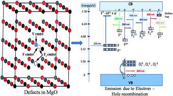
A detailed investigation on different defects from induced emission characteristics in MgO, which are responsible for the multicolor emissions and lasing property of that material, is presented in this report. The color centers are characterized by absorption spectroscopy, decay kinetics, and a TRES study. Various defect centers such as oxygen vacancies (e.g., F, F+,
,
,
), cationic vacancies (
,
,
), interstitial oxygen (
,
,
), Schottky defect
, etc., create different electronic states inside the wide band gap. Density Functional Theory (DFT) based calculation was performed for these defect centers to characterize their ground electronic states inside the band-gap. In MgO, a photo ionization process of the F center is involved at an excitation wavelength of 250 nm, followed by the equation F + hν ↔ F+ + e. The released electron in this process may prompt into the conduction band and thereby behaves as a free carrier. Being free, the electron may recombine with different types of positively charged defect centers in addition to the newly formed F+ centers. Thus, different electronic transitions from the conduction band (CB) to the empty ground electronic states of positively charged F- and F2-type centers can be correlated with their observed emission components. Recombination of a hole in the valence band (VB) with a filled electron in the electronic states may also be responsible for some emission behaviors. Thus, an understanding about all the emitting color components due to various defect centers in MgO might be possible by considering those special recombination processes and may also help to remove the long standing contradiction regarding their origin.
1. Introduction
Although defects are generally considered as imperfections in an inorganic matrix, they are not always disadvantageous and sometimes they may lead to some attractive material properties such as optical, magnetic, catalytic, energy conversion, etc.1–5 For a long time, it has been known that defects play large roles in determining optical properties of wide band gap crystalline materials; these are interesting for various technological applications such as adsorbents, sensors, catalysis, refractory material, paint, fluoride remover, optoelectronics, and luminescence devices.6–9 A recent literature survey shows that defect-induced photoluminescence (PL) is a hot topic in various activator free oxide materials such as ZnO, TiO2, SnO2, Al2O3, and MgO10–15 etc. These semiconductor or defect-related materials are potential alternatives to traditional metal activator based phosphors, because of their advantages of low toxicity, stability, tunable emission color, and low cost. In our laboratory too, various kinds of defect-induced emissions were very recently observed in different oxide based materials, such as in spinels, perovskite, molybdate, tungstate, etc.16–23 Different kind of defects such as anionic and cationic vacancies, impurities, radical impurities, donor–acceptor pairs, etc. may evoke charge imbalances at the defect sites which are rectified by localization of electrons and electron holes, and which may give rise to different electronic states within the band gap. These electronic states within the band gap are apparently precursors for various emission centers of defect-related materials and impart them with excellent photoluminescence characteristics.
Wide band gap insulator MgO with a band gap of 7.8 eV has shown a lot of interest in recent years due to its exceptional optical, magnetic, and electronic properties.24–27 Photoluminescence (PL) spectra of MgO nanomaterials are reported to be due to various structural defects, such as oxygen vacancies, Mg vacancies (F-center defects and V center defects), and interstitials.24,28,29 Though it is a wide band gap material,30 presence of different kind of intrinsic/extrinsic defect-induced states within the band gap reduce the photon excitation energy of this material significantly well below the band gap energy.31 A detailed investigation on trapping and recombination processes of F-type centers (F & F+ center) and their lasing property in MgO microcrystals was reported by T. Uchino's group recently.32–34 Since these defects are also linked with the material's size distribution, surface chemistry, phase, morphology, and/or porosity, a band gap engineering of these nanostructures is also possible with varying synthesis methodology (e.g., heat treatment), which in turn will affect the physical properties of the particles such as optical, magnetic, catalytic, etc.
Both in monovalent alkali halide (e.g., NaCl) and divalent oxide (e.g. MgO) with rock salt cubic crystals,14 the main defects are anion or cation vacancies called F or V centers, possessing various charged states with trapped electrons or holes. In monovalent alkali halides there is a good understanding about these kinds of vacancies, and that the F centers are responsible for the lasing property,35 but in divalent MgO there is still some controversy about these defects regarding their position within the band gap and interaction with the excitation.36,37 Recently, Rinke et al. have shown an agreement between the calculated and the experimentally observed absorption and emission spectra of F0 and F+ centers in MgO.38 However, in addition to these two defect centers, several other defect centers are also possible. Defects such as doubly positive charged oxygen vacancies (F2+ or
), cluster of F+ centers such as
,
[pair of adjacent F and F+ centers such as (F+ + F+) or (F + F+)], cationic vacancies
, hole trap at cationic vacancies
, interstitial oxygen (
,
&
), and Schottky defects (which form when oppositely charged Mg2+ and O2− ions leave their lattice sites and form MgO molecules), etc. also exist in MgO. Information regarding their electronic structures within the electronic band gap and its impact on the optical properties is still missing in the literature. In this regard, a correlation study of the observed optical properties with DFT calculated spin states due to various kinds of defect states will provide a great deal of understanding about defect-induced optical properties of MgO, which otherwise is not possible except through experimental means. Rosenblatt et al.28 reported that in MgO, the F center undergoes a photo conversion process F + hν (250 nm) ↔ F+ + e− at an excitation wavelength of 250 nm, and since the excited state was very close to the conduction band (only 0.06 eV below the conduction band),28 the released electron during this conversion becomes free and can go to the conduction band (CB). Therefore, the electron will behave as a free carrier and the recombination process with the hole does not necessarily occur at the same site where it was created. Other positively charged defect centers such as F+ and F2+ centers (which might be created by a photo bleaching process or were already present in the compound) will naturally attract the free electron followed by a recombination process.38 Similar kinds of recombination process are also possible for positively charged F2-type centers such as
,
, and
centers. These defect centers may be created by photo conversion of a F center present in the pair form such as F2 and
centers at 250 nm excitation or may be present intrinsically in the compound. Since at 250 nm excitation wavelength, the recombination process of the free electron will occur from the CB, we don't have to consider the excited electronic states of the various defect centers. Thus, with the help of a density functional theory (DFT) calculation, if we characterized different filled and unfilled ground electronic states due to various defects, a detailed understanding of all the emission components is achievable by considering various possible ways of recombination of the free electron (which resulted due to the photo conversion of a F center at 250 nm) in the CB with the ground state of one electron left in positively charged defect centers (generated either by photo bleaching or exists intrinsically). Reports in this context are yet to be published in MgO. Further, this study will also open a new way of understanding the defect-related emission behaviors in many compounds where a photo conversion process exists at a certain wavelength and the released electron is prompted to the conduction band (CB).
Therefore, the present study reports a detailed investigation on the formation of different defect states in MgO and their correlation with multicolor emission behaviors. The MgO compound was derived through a sol–gel method followed by characterization with X-ray diffraction (XRD) and scanning electron microscopy (SEM). Absorption spectroscopy indicates presence of different defect states in the material. With the help of lifetime measurements and Time Resolve Emission Spectroscopy (TRES), various kinds of defects induced color components were identified and isolated from the complex emission spectra. As prepared MgO was further annealed at different higher temperatures and the respective emission spectra were deconvoluted into different color components using Gaussian fitting, as observed from the TRES study. This helped to monitor the change of individual color components at different annealing temperatures. DFT calculations were performed using projector augmented wave potential and generalized gradient approximation for different kinds of charged and neutral defects as mentioned earlier. From the DFT calculated density of states (DOS) a clear understanding about the electronic structures inside the band gap due to different defect states, and their correlation with observed emission characteristics, was successfully achieved, which removes a long standing contradiction about the origin of different color centers in MgO.
2. Experimental
2.1 Synthesis
MgO compounds were synthesized by the thermal decomposition of magnesium oxalate precursor39 which was synthesized through a sol–gel method using magnesium nitrate hexahydrate [Mg(NO3)2·6H2O] and oxalic acid as precursors in a 1
:
1 molar ratio. At first, two clear solutions of [Mg(NO3)2·6H2O] and oxalic acid were made by dissolving them separately in ethanol. These two solutions mixture were then mixed with continuous stirring for 2 h and a thick white gel was observed. The gel was then heated at 100 °C for 8 h followed by grinding to get fine powder of magnesium oxalate. The oxalate product was then decomposed at 600 °C for 6 h to obtain magnesium oxide (MgO-600) followed by characterization using XRD and TEM. After confirming the formation of the product, the compound was further annealed at higher temperature such as 800 °C (MgO-800) and 1000 °C (MgO-1000). The detailed instrumental technique is provided in the ESI.†
2.2 Computational methodology
All the electronic structure calculations of various defects in MgO were performed by spin-polarized plane wave based density functional theory (DFT) as implemented in a Vienna Ab-initio Simulation Package (VASP).40,41 The interactions between electrons and ions is described using a projector-augmented wave (PAW) method42 which includes the valence states of Mg (3s – 2 valence electrons) and O (2s, 2p – 6 valence electrons). Generalized gradient approximation (DFT-PBE) was used for the exchange–correlation potential in the form of Perdew–Burke–Ernzerhof (PBE).43 A 2 × 2 × 2 supercell (64 atoms) was employed to study defect formation in MgO. For calculations of the unit cell (8 atoms) and 2 × 2 × 2 supercell (64 atoms), integration over the Brillouin zone was carried out on 16 × 16 × 16 and 8 × 8 × 16 k-point meshes generated using the Monkhorst–Pack44 method; both are proven to be sufficient for energy convergence of less than 0.1 meV per atom. A cutoff energy (Ecut) of 500 eV for the plane wave basis set was used. For cubic MgO unit-cell, optimization of Ecut and k-point meshes were carried out to ensure convergence of total energy to within a precision of 0.1 meV per atom. The total energy of a MgO unit cell as well as supercells were optimized with respect to volume, shape, and atomic positions as permitted by the space-group symmetry of the crystal structure. Structural relaxations were performed for each defect structure using the conjugate gradient algorithm until the residual forces and stress in the equilibrium geometry were of the order of 0.005 eV Å−1 and 0.01 GPa, respectively. The final calculation of total electronic energy and density of states (DOS) were performed using the tetrahedron method with Blöchl corrections.45
3. Results and discussion
3.1 Structural and morphological characterization
3.1.1 Phase purity: X-ray diffraction (XRD). Fig. 1 shows the XRD patterns of the MgO compounds prepared at different annealing temperatures which indicates that all the patterns correspond to the cubic (NaCl-type) periclase phase of MgO with the known lattice parameter, a = 4.211 Å [JCPDS 45-946]. The diffraction peaks of MgO-600 are somewhat broader and when the annealing temperature increased they become sharper.
 |
| Fig. 1 XRD patterns of MgO compounds: (a) MgO-600, (b) MgO-800, and (c) MgO-1000. | |
3.1.2 Morphology study: SEM. Fig. 2a and b shows the scanning electron microscope (SEM) micrograph of as prepared MgO sample and high temperature annealed sample, respectively. The micrograph of as prepared samples depicts a thin flake like morphology oriented in clustered vertical geometry. The average particle size of as prepared MgO flakes is around 0.4 micron. Such flakes with highly porous network can create a new pathway in the field of electrocatalysis. Once samples are annealed at higher temperature, then flakes start disintegrating into crumbled powder and begin agglomerating in a random orientation with an average size around 1.0 micron.
 |
| Fig. 2 SEM images of (a) MgO-600 and (b) MgO 1000 compounds. | |
3.2 Absorption spectroscopy
The UV-visible spectra of MgO-600, MgO-800, and MgO-1000 are shown in Fig. 3 in the reflectance mode. Since the lower spectral detection limit of the UV-Vis spectrophotometer is 200 nm, any absorption or reflectance below 200 nm cannot be detected. There are several absorption peaks in the UV and visible region which indicates presence of defects and low coordinated cations and anions on the surface, interface, etc.29 Absorption at 207 nm is due to the excitation of 5 coordinated surface anions while the excitation at ∼240 nm and ∼250 nm are due to F+ and F centers, respectively.46,47 The absorption peak at 313 nm can be ascribed to the
centers.39,46 The absorption at 450 nm is due to the transition of a four coordinated F center.48 The net decrease in absorbance with annealing was due to decrease of defect concentration.
 |
| Fig. 3 UV-visible spectrum (in reflectance mode) of (a) MgO-600, (b) MgO-800, and (c) MgO-1000. | |
3.3 Photoluminescence spectroscopy
3.3.1 Excitation spectroscopy. Fig. S1† shows the photoluminescence excitation (PLE) spectrum of as prepared MgO-600 at λem = 540 nm. The PLE spectrum consists of some intense lines near 230, 247, 258, 271, 285, 297, 310, and 345 nm. Presence of several PLE peaks indicates presence of different types of defect states inside the band gap. Peaks in the 230–270 nm range are assigned to different types of F and F+ centers49–51 while peaks at 285, 310, and 340 nm can be attributed to their aggregates such as F2 and
centers.49
3.3.2 Emission spectroscopy. Emission spectra at different excitation wavelengths are presented later (in Fig. 16) where we have seen an increase in intensity of the emission spectra at 250 nm, which is due to a photo conversion process of the F center as reported earlier.28,29,38,39 Since we are interested in the photo conversion process of the F center at and its consequence on the different defect-induced emission characteristics, all the emission spectra were recorded at excitation wavelength of λex = 250 nm (≈247 nm). Fig. 4 represents the room temperature PL spectra of MgO-600, MgO-800, and MgO-1000 compounds. The overall intensity decreased when the samples were annealed at higher temperatures. This indicated a decrease in concentration of the defect states responsible for the host emission. More decay in intensity was observed in the near infrared (NIR) region (750–900 nm) and orange-red (605 nm) region while intensity of the blue region (450 nm) was found to decrease for MgO-800 followed by increase in the case of MgO-1000. Emission profiles clearly indicate presence of several color centers in the MgO matrix, resulting in emissions at different wavelengths in the visible and IR regions. These emission spectra are composed of emission peaks at around 390 nm, 450 nm, 490 nm, 540 nm, 605 nm, 680 nm, and 850 nm respectively. To get a clear view of these emission components, we have carried out their life time measurement and time resolve emission spectroscopy (TRES).
 |
| Fig. 4 Emission spectra of (a) MgO-600, (b) MgO-800, and (c) MgO-1000 at λex = 250 nm. Arrows show peak positions of different emitting components which may slightly shift towards the right hand or left hand side at different annealing temperatures. | |
3.3.3 Lifetime study. Fig. 5 shows the luminescence decay profile of the as prepared MgO-600 compounds at different emission wavelengths viz., λem = 390, 450, 490, and 540 nm at an excitation wavelength of λex = 250 nm. Decay profiles at λem = 605, 680, and 850 nm are given in Fig. S2.† The decay curves were fitted into a mono or bi or try exponentials using the following decay eqn (1)–(3) |
I(t) = A0 + A1 exp(−t/τ1)
| (1) |
|
I(t) = A0 + A1 exp(−t/τ1) + A2 exp(−t/τ2)
| (2) |
|
I(t) = A0 + A1 exp(−t/τ1) + A2 exp(−t/τ2) + A3 exp(−t/τ3)
| (3) |
where t is the time, and τ1, τ2, and τ3 are decay time values for exponential components and A0, A1, A2, and A3 are scalar quantities obtained from the decay curve fitting. The bi and tri exponential behavior of some of the decay components indicates that there is an overlap, by either the preceding one or by the next band or by both, and therefore a multi exponential decay equation was observed instead of mono exponential. In those cases the life time value with the highest percentage of contribution was considered to have originated from the monitoring wavelength. The decay times (τ1, τ2, and τ3) for various color components viz. 390, 450, 490, 540, 605, 680, & 850 nm with their respective percentage contributions are given in Table S1 in ESI.† Therefore, lifetime values as obtained from Table S1† for different color components are: 11.22 μs (390 nm), 13.54 μs (450 nm), 212.2 μs (490 nm), 82.48 μs (540 nm), 15.09 μs (605 nm), 362 μs (680 nm), and 13.23 μs (850 nm) respectively.
 |
| Fig. 5 Decay profiles of the MgO-600 compound at λex = 250 nm and at different emission wavelengths viz. (a) 390 nm, (b) 450 nm, (c) 490 nm, and (d) 540 nm. | |
3.3.4 Time resolved emission spectroscopy (TRES). Fig. 6 shows TRES at different delay times such as 2 μs, 20 μs, 40 μs, 100 μs, 200 μs, 500 μs, and 900 μs, with a constant integration time of 1 ms while Fig. 7 shows the TRES spectra of individual emission components derived from Fig. 6 following our earlier procedure.16,52 Generally, all the excited species use to be fully decayed at an average time, which is approximately three times of their respective life time (3τ). Therefore, at very low delay times such as at 2 μs, we can assume that none of the color components will be completely decayed since none of them have a lifetime below 2 μs as shown in Table S1.† However, as we kept on increasing the delay time, the short-lived components were decayed first, followed by the long lived ones. From Table S1,† the different components in increasing order of their life times are 11.22 μs (390 nm) < 13.23 μs (850 nm) < 13.54 μs (450 nm) < 15.09 μs (605 nm) < 82.48 μs (540 nm) < 212.2 μs (490 nm) < 362 μs (680 nm) etc. Therefore, in the time interval of 2–20 μs, the species which started decaying have lifetime values of 11.22 μs, 13.23 μs, 13.54 μs, and 15.09 μs. This is also supported by the observed decay in intensity in the 390 nm, 450 nm, 605 nm, and 850 nm regions as we increased the delay time from 2 μs to 40 μs. Again, since the 390 nm color component had the lowest lifetime of 11.22 μs, in the time interval of 2–20 μs, it will decay more as compared to others. On the contrary, in the time interval of 20–40 μs, the other components, such as 450, 605, and 850 nm with comparatively higher life times will be the prominent decaying components. This is also reflected in the Fig. 7a where we have subtracted the TRES spectra at a 2 μs delay time with that at 20 μs and in Fig. 7b where the TRES spectra at a 20 μs delay time was subtracted from that at a 40 μs delay time. For further clarification, Gaussian-fitted spectra of Fig. 7a and b are provided in Fig. S3 and S4.† In Fig. S3,† we can see that in the time interval of 2–20 μs, the P1 (∼390 nm) component, was decaying more in comparison to the P2, P5 and P7. On contrary in Fig. S4,† in the time interval of 20–40 μs, the contribution of P1 was negligible and the main decaying components are P2, P5 and P7. The next color component with higher lifetime is 540 nm (82.48 μs) and we saw a comparatively larger decrease in intensity in this wavelength region in the time interval of 100–300 μs, as shown in Fig. S5.† The next longer-lived species is 490 nm (212.2 μs) and we saw a decrease in intensity in the respective wavelength region at higher delay times, such as in the time interval of 300 to 600 μs. We must mention that in the 100–300 ms time interval along with the 540 nm; the 490 nm species also started decaying and if we subtract TRES at 100 μs with that at 300 μs time, the resulting TRES will be composed of both the 490 and 540 nm components with the major contribution from the latter as shown in Fig. 7d. The Gaussian fitted spectra of Fig. 7d are represented by Fig. S5,† which showed that P3 (∼490 nm), P4 (∼540 nm), and P5 (∼605 nm) are major decaying components in the 100–300 μs time interval, with the major contribution coming from P4 (∼540 nm). However, in the higher decay time interval, such as in the 300–600 μs in Fig. 7e, the resulting TRES after subtraction will consist of mostly 490 nm emission, since the next long-lived species, 680 nm (362 μs), will not completely decay in this time region. Gaussian fit of Fig. 7e is presented in Fig. S6,† which shows that in the time interval 300–600 μs the major decaying component is P3 (∼490 nm). Along with P3, some P4 (∼540 nm) components also decayed in the initial portion of this time interval as shown in that figure. However, no P6 (∼680 nm) component was found to decay in this time region due to its higher lifetime value. A constant decrease in intensity at 490 nm compared to that at 680 nm can also be seen at higher delay times such as 900 μs in Fig. 6g. One Gaussian fit TRES spectrum at 800 μs is presented in Fig. S7† which clearly shows presence of two components, P3 (∼490 nm) and P6 (∼680 nm), at higher delay times with the major contribution coming from P6 (∼680 nm). Gaussian fits of Fig. 7f and g are shown in Fig. S8 and S9.† All these fitting spectra clearly support those emitting components.
 |
| Fig. 6 TRES at different time intervals. | |
 |
| Fig. 7 TRES due to different color components. | |
Now from the TRES study, we can isolate the different color components at 390, 450, 490, 540, 605, 680, and 850 nm from the complex emission spectra, as shown in Fig. 6 and 7. Since the luminescence processes involve a Gaussian line broadening mechanism, the emission curves of MgO-600, MgO-800, and MgO-1000 compounds were deconvoluted16 and decomposed to the different color components which are violet at λmax ≈ 390 nm (P1), indigo at λmax ≈ 450 nm (P2), blue at λmax ≈ 490 nm (P3), green at λmax ≈ 540 nm (P4), Orange at λmax ≈ 605 nm (P5), orange-red at λmax ≈ 680 nm (P6), and the NIR region at λmax ≈ 850 nm (P7), as shown in Fig. 8. From the deconvoluted spectra, several observations can be made on these individual emission components. The intensity of the P1 band decreased while that of P2 to increased compared to each other. The other color components where a prominent decrease in peak intensity was found are P3, P5, and P7. Now, to explain the origin of all these emission components, let us first discuss the ground sate electronic structures inside the band gap of MgO arising due to different kinds of charged and uncharged vacancies.
 |
| Fig. 8 Gaussian fit of the emission profiles of (a) MgO-600 (b) MgO-800 and (c) MgO-1000 compounds. | |
3.4 Electronic structure and band gap energy
Multicolor emissions of pure MgO compounds indicate the presence of various electronic states within the band gap of the materials, where each color arises due to a different electronic transition. These electronic states must originate from various defect states, otherwise, in a wide band gap material like MgO (band gap ≈ 7.8 eV), these color components in the visible region would not have been possible. To get an insight about the electronic structure inside the band gap, the individual ground electronic states of various neutral and charged defect centers were calculated using a DFT calculation. We considered most of the possible neutral and charged single anionic vacancies (F-type centers) and their clusters (F2-type centers) e.g., F (or
), F+ (or
), F2+ (or
),
(or
),
(or
),
(or
); cationic vacancies e.g.,
,
,
, and Schottky defect
; interstitial oxygen e.g.
,
, and
etc. MgO crystallizes in the rock-salt structure, where each atom is six-fold coordinated in the bulk. The experimentally determined lattice constant for MgO is 4.207 Å at T = 0 K (ref. 53) which matches well our DFT-PBE calculated lattice constant of 4.238 Å. Fig. 9 shows the location of these defects in a 64 atom supercell which was employed in our DFT calculations.
 |
| Fig. 9 Location of the lattice vacancies in a 64 atom MgO supercell. V centre presents location of the Mg vacancy (blue atom, , , and ). F centre presents location of the O vacancy (empty dotted sphere, , and ). F2 centre presents an oxygen di-vacancy with different charges ( or , or , or , etc., vacancy clusters). In the case of P centre (neutral Mg + neutral O vacancy) Mg and O vacancy sites are V centre and F centre, respectively. Red and black atoms present O and Mg ions, respectively. | |
DFT-PBE calculated partial and total density of states (DOS) of an ideal MgO crystal in Fig. 10a clearly shows that the valence band (VB) is composed of Mg s as well as p states while the conduction band (CB) is composed of p-states of both Mg and O. The bonding type in MgO is strongly ionic, with formal ion charges of magnesium and oxygen which are 2+ and 2−, respectively. Our DFT-PBE calculated electronic band-gap is 5.09 eV which is underestimated compared to the experimental band gap of MgO at 7.8 eV.30 Defects such as intrinsic point defects, impurities, and defect complexes are not only responsible for the color of the samples, but can also give rise to electron or hole conductivity.54,55 This study tries to investigate the effect of all possible defects on the electronic structure of MgO. During comparison of the defect structures, it was expected that the DFT-PBE calculated band-gap error would be cancelled. Underestimation of band-gap is a well known limitation of the DFT-PBE.16,19–21
 |
| Fig. 10 Total density of states (DOS) and species projected DOS for (a) pure pristine MgO crystal and with (b) F0, (c) F+ and (d) F2+ centers calculated for a 64-atom supercell using DFT-PBE. Vertical lines at zero energy represent Fermi energy and DOS for spin-up (spin-down) states are shown in red (blue). | |
Removing an oxygen atom from the ideal MgO lattice generates a defect state which can be filled by 2 (F0), 1 (F+), or 0 (F2+) electrons. When an oxygen atom is removed from the MgO lattice, the arrangement of atoms in the vicinity of the defect will adjust to lower the energy of the system. For the neutral F center (F0), where two electrons remain at the defect site, the displacement of atoms is not very pronounced since the defect electron distribution resembles the electron distribution around an O2− anion. Removing one or both of the defect electrons leads to a more distinct geometric relaxation. The Mg2+ ions close to the positively charged oxygen vacancy are repelled, while the O2− lattice ions feel an attraction. For the neutral F0 center, only the nearest neighboring atoms are involved in the geometric relaxation. For charged defects, also next-nearest neighbors contribute to the geometric relaxation around the oxygen vacancy. There is no symmetry-breaking in either case, which was also tested by starting the relaxation from a geometry with broken symmetry using DFT-PBE exchange–correlation functionals. The geometric relaxation for all relevant charge states are quantified in Table 1. The equilibrium DFT-PBE calculated bulk distances between magnesium and oxygen atoms near the oxygen vacancy site are listed together with the relaxed distances for the F0, F+, and F2+ centers. There is an inward relaxation of nearest-neighbor oxygen atoms for F2+ and F+ centers, while for the F0 center a weak outward relaxation of both nearest-neighboring oxygen atoms takes place. DFT-PBE calculated equilibrium volume shows an increase of 2.15 Å3 for F0 as well as decrease of 7.47 Å and 15.35 Å for F+ and F2+, respectively.
Table 1 Unit-cell volumes, distances between Mg and O atoms (1st and 2nd nearest neighbor (NN), nearest to the vacancy site) of bulk MgO and systems with oxygen vacancies
Defects |
Change in unit cell volume (Å3) |
Distance between 1st and 2nd NN Mg–Mg (Å) |
Distance between 1st and 2nd NN Mg–O (Å) |
Defect free |
0 |
3.00, 3.00 |
2.12, 2.12 |
 |
+2.15 |
2.99, 3.00 |
2.11, 2.13 |
 |
−7.47 |
2.93, 2.99 |
2.02, 2.09 |
 |
−15.35 |
2.87, 2.98 |
1.94, 2.06 |
The most prominent feature in the electronic structure of F centers in MgO is a highly localized defect state. For the neutral defect, this state is occupied by two electrons. By removing one or two electrons from the defect level, singly- or doubly-charged oxygen vacancies can be created. The DFT-PBE calculated DOS for bulk F centers show the defect level as a flat energy band close to midgap (Fig. 10b). For the F+ center, the two spin channels are considered separately, since the two defect spin states are no longer degenerate. Projecting density of states (DOS) on the basis of individual atoms in the system, it is shown that the defect level is mainly due to magnesium s and p states. The defect states as shown by arrows in the total DOS curves are located 2.3 eV (for F0, Fig. 10b), 1.88 eV (for the occupied spin states for F+, Fig. 10c), 3.29 eV (for the unoccupied spin states for F+, Fig. 10c), and 2.59 eV (for the unoccupied spin state of F2+, Fig. 10d) away from the VB maxima in the electronic band-gap.
Fig. 11 shows DFT-PBE calculated total and species projected DOS for the pristine MgO crystal with neutral Mg vacancy
(Fig. 11a), −1 charged Mg vacancy
(Fig. 11b), and −2 charged
Mg vacancy (Fig. 11c). Effect of Mg vacancy (neutral and charged) in the DOS is very weak. No filled and unfilled spin states are observed inside the band gap for all the type of charges. In all cases, overall DOS features remain the same but shallow defect states are generated very close to VB maxima and CB minima.
 |
| Fig. 11 Total density of states (DOS) and species projected DOS for MgO crystal and with (a) Mg vacancy , (b) −1 charged , and (c) −2 charged Mg vacancy, calculated for a 64-atom supercell using DFT-PBE. Vertical lines at zero energy represent Fermi energy and DOS for spin-up (spin-down) states are shown in red (blue). | |
Fig. 12 shows the DFT-PBE calculated total and species projected DOS for the pristine MgO crystal with different vacancy clusters such as (a) Mg–O vacancy cluster (
or P centre) and oxygen di-vacancy cluster with different charges e.g., (b)
, (c)
and (d)
, respectively. In the case of a Mg–O vacancy cluster (P center) (Fig. 12a), the DFT-PBE calculated DOS resembles a DOS of
. Different spin states arising inside the band gap are shown by arrows in the total DOS. One vacant spin state was observed 2.24 eV away from the valance band. For the F2 type of centers 4 spin states are generated in each case. For a
center (Fig. 12b), two spin up (1.73 & 2.596 eV from the VB, respectively) and one spin down (2.249 eV from the VB) states are occupied while the fourth spin down state (3.46 eV from the VB) is empty. For
centers (Fig. 12c), two spin up (1.55 & 2.42 eV from the VB, respectively) states are occupied and two spin down states (2.94 & 3.97 eV from the VB, respectively) are unoccupied. Overall nature of the DOS is similar to the DOS of
. For
centers (Fig. 12d) the first spin up state (1.55 eV from the VB) is occupied while the 2nd spin up (2.59 eV from the VB) and the remaining two spin down states (2.76 & 3.63 eV from the VB) are unoccupied.
 |
| Fig. 12 DFT-PBE calculated total and species projected DOS for the pristine MgO crystal with (a) a neutral Mg–O vacancy cluster ( , P centre), (b) centers, and (c) & (d) , respectively, calculated for a 64-atom supercell using DFT-PBE. Vertical lines at zero energy represent Fermi energy and DOS for spin-up (spin-down) states are shown in red (blue). | |
Fig. 13 shows the DFT-PBE calculated total and species projected DOS for the MgO crystal with different charged interstitial oxygen atoms such as neutral oxygen interstitial
(Fig. 13a), −1 charged oxygen interstitial
(Fig. 13b), and −2 charged oxygen interstitial
(Fig. 13c). Different spin states inside the band gap are shown by arrows in the total DOS. For neutral oxygen interstitial
, two closely located spin up occupied states (0.612 eV from the VB) and two closely located spin down occupied states (1.224 eV from the VB) near the Fermi energy level were observed (Fig. 13a). For −1 charged oxygen interstitial
, one spin down occupied state (0.20 eV from the VB), two closely located spin up occupied states (0.91 eV from the VB), and another pair of closely located spin down occupied states near the Fermi energy level (1.377 eV from the VB) were observed (Fig. 13b). For −2 charged oxygen interstitial
, two occupied spin states (0.30 eV & 1.68 eV from the VB, respectively) were observed (Fig. 13c). From the figure, some shallow empty states also exist, because of which the CB is narrowed down.
 |
| Fig. 13 Total density of states (DOS) and species projected DOS for MgO crystal with (a) neutral oxygen interstitial , (b) −1 charged oxygen interstitial , and (c) −2 charged oxygen interstitial calculated for a 64-atom supercell using DFT-PBE. Vertical lines at zero energy represent Fermi energy and DOS for spin-up (spin-down) states as shown in red (blue). | |
So the following summary can be drawn from the above density of states, observed from DFT based calculations for different kinds of charged and uncharged vacancies and vacancy clusters viz.
(F0),
(F+),
(F+),
,
,
,
(V0),
(V1),
(V2−), and
(P, Schottky), as represented pictorially in Fig. 14. It is worth noting that for all these calculation, DFT-PBE calculated electronic band-gaps for different calculations are less than the experimental band gap of bulk MgO, which is around 7.8 eV for the bulk compound.30,56,57 Therefore, in order to correlate experimentally observed emission components with the electronic structure of MgO, we need to multiply the energy of the spin states present inside the band gap with the factor
. After multiplying by the suitable factors, the different electronic states with their respective energy position in the actual band gap are shown in Fig. 14. All the electronic states represent the ground state configuration. The figure shows different filled (represented by bold) and unfilled (represented by white color) electronic states inside the band gap arising due to different kinds of vacancies in the matrix. These spin states represent a ground state configuration and the excitation of the electron will be from the filled electronic state. Similarly, the emission of certain defect states is associated with the transition of an electron from the excited state to the unfilled electronic state in the ground state configuration. Although the present DFT study does not deal with excited states due to some restrictions, fortunately the excited states of F and F+ centers lie very close to the conduction band and there is a photo conversion process of F to F+ centers involved at 250 nm following the equation F + hν ↔ F+ + e−.28,29,38,39 Since the absorption bands of these two species are also energetically close,48,58 any of them cannot be excited without exciting the other. The F+ center is thus considered as the ionized state of the F. The released electron during this conversion becomes free and behaves as a free carrier. Therefore, the recombination process of this free electron with a hole does not need to occur at the same site where they were created. Other positively charged defect centers such as F+, F2+,
,
,
, etc. centers (which might be created by a bleaching process or were already present in the compound) will naturally attract the free electron and the recombination process may occur with them.38 The free electron can also be trapped into a different trap state (vacant electronic state) within the band gap. The F center emission can therefore be realized by a recombination process of the free electron in the conduction band with the vacant spin state with the F+ center in the ground state, following the equation F+ + e ↔ F + hν.28,38 Similarly, if the electron in the filled electronic state of a F+ center is photo-excited to the conduction band, then the resulting ground state will be like a F2+ center and, on encountering the free electron in the conduction band, the F+ center emission can be realized by the equation F2+ + e ↔ F+ + hν.39 On a similar line we can also say that the
and
center emission can be realized by considering the recombination process of the free electron in the conduction band with the unfilled ground state of
and
respectively, following the equations
and
, respectively. Thus, the energy difference between the bottom of the conduction band and the unfilled electronic state of F+ will be the energy of the radiative emission of F center. Similarly, the energy difference between the conduction band and the unfilled electronic state of
,
, and
will be emitted in the form of radiative emission due to F+,
, and
centers, respectively. The reverse recombination process i.e., a free hole in the valence band with the filled state of F center is also possible (a positively charged F center will be repelled by the hole) if at the 250 nm excitation wavelength some electrons are knocked out from the VB to the upper excited state inside the band gap due to different defect states. Therefore, Fig. 14 will help with a great deal of understanding about the correlation of the observed emission components with different defects from induced electronic states inside the band gap.
 |
| Fig. 14 Overall summary of the location of oxygen defect states arising due to (F0), (F+), and (F2+) as well as Mg defect states arises due to , , and . Distribution of defect states for vacancy cluster's F2 centre and P centre are also summarized. Color filled bands are filled with electrons and white bands are empty. | |
Now let us explain all the color components present in the emission profile and their correlation with the band gap electronic structure by proposing a model of electronic transition in Fig. 15. The recombination processes of the respective emissions are also listed in Table 2. The model in Fig. 15 shows different filled and unfilled electronic states of the concerned defects which are responsible for the excitation and electron–hole recombination process at 250 nm excitation. A photo conversion process at 250 nm is shown followed by release of an electron. The electron can go to the conduction band as shown by a green arrow and thus behaving as a free carrier, which can now recombine with different positively charged F and F2 type centers in their ground states. A recombination process of a free hole in the VB with the electron in the filled negatively and neutral interstitial oxygen atom is also shown at the bottom of the model. A comparison of emission energies obtained from our calculations and experiments for some of the defect centers, with their previously reported values, will also successfully justify our proposed model of electronic transitions as given in Fig. 15. As reported in the literature, the violet emission (P1) at λmax ≈ 390 nm could be assigned to the F+ center while the green emission (P4) at λmax ≈ 540 nm is due to F center.28,29,32–34 From our DFT calculated DOS, as summarized in Fig. 14, we can see that there are two vacant empty states for F+
and F2+
centers, with the later one lying below the former one. The energy difference of these two states with the conduction band are ∼2.4 eV for F+ center's vacant state while, for F2+ center's vacant state, it is ∼3.5 eV. These theoretically observed energy differences may not exactly match the experimental values 2.3 eV (∼540 nm) & 3.2 eV (∼390 nm), but they fall very well within the very broad experimental peak. Thus, the violet emission (P1) at λmax ≈ 390 nm is assigned to the F+ center owing to the encounter of the free electron in the conduction band with the F2+ center following the equation F2+ + e ↔ F+ + hν (390 nm) as represented in Fig. 15 by violet color. Similarly, the green emission (P4) at λmax ≈ 540 nm can be assigned to the F center following the electron encounter equation F+ + e ↔ F + hν (540 nm), represented in Fig. 15 by green color. From a formation energy point of view also, these centers (F & F+) are likely to be present in the system. The higher life time value of a F center than the F+ center can be explained by considering ionization of the F center to F+ followed by recapture of electron.34 Similarly, the energy difference between the conduction band and the higher vacant state of
state is ∼2.8 eV which closely resembles the indigo (P2) emission at λmax ≈ 450 nm (2.81 eV). Thus, this emission can be assigned to the
centers as reported in earlier literature references,31,33 following the electron encounter equation
(450 nm) in the proposed model by indigo color. Next, the energy difference between the conduction band and the vacant state of
center is ∼1.8 eV which is very close to the red emission at λmax ≈ 680 nm (P6). Here the
center is considered as a pair of F and F+ centers and the F center may undergoes a photo conversion process at 250 nm, thereby forming
centers. Therefore, the red (P6) emission originates from the
, followed by the recombination process
(680 nm). The higher life time value of
centers compared to the
centers can be explained on the same basis as that of F and F+ centers. According to literature, the blue emission (P4) at λmax ≈ 490 nm (P3) may be assigned to a hole trapped at a Mg ion vacancy.29 Since, from our calculation of DOS for various charged Mg vacancies, such as
,
(hole trap at
), and
, we have not observed any vacant states, recombination of an electron from the CB with the hole trap at Mg vacancies is not possible. Negatively charged cationic vacancies also repel the free electron. Recombination of a positively charged hole in the VB with the electron in the filled electronic state is also ruled out in this case, since the resulting emission will be of very low energy. However, if we consider spin states of the
center, a vacant spin state at ∼2.58 eV (∼480 nm) below the conduction band is found to exist. Therefore, the blue emission at λmax ≈ 490 nm (P3) can be assigned to the F2 centers followed by the recombination process
(490 nm). The energy difference also closely resembles this emission. A vacant state at ∼4.16 eV below the conduction band due to the
(P, Schottky) center is also present. However, due to a huge energy difference with the observed blue emission at λmax ≈ 490 nm (P3) (2.53 eV), this emission cannot be due to recombination of the free electron with this vacant state of a P center. Since the orange emission at λmax ≈ 605 nm (P5) is drastically reduced at higher annealing temperatures, we believe they must have originated from some kind defects which annealed significantly at higher temperatures. As can be seen from Fig. 8, with increasing annealing temperature, there is a decrease in the F+ center emission. However, the energy difference of the conduction band with the vacant state of F+ center does not match with the observed emission; rather it matches with some shallow trap state. From our calculation we can see the presence of different shallow trap states due to interstitial oxygen atoms. Therefore, transition from some shallow trap state to the oxygen vacancies
might be responsible for this emission. At a higher annealing temperature, decrease in the intensity can be explained both in terms of decreasing concentration of
and
, since the interstitial oxygen atom will recapture its normal lattice sites. The broad emission in the NIR region with λmax ≈ 850 nm (P7) (1.45 eV) cannot be explained by considering any transition of the free electron from the CB or a trap state to the vacant spin states of the defects, since none of the energy differences match this low energy emission (1.3–1.6 eV). However, a reverse combination process i.e., a hole at the VB and an electron in the defect states may explain this broad band emission.38 The hole at 250 nm excitation wavelength may be created by knocking out one electron to form vacant excited states inside the band gap or it may be created by a two photon excitation phenomenon. As shown in Fig. 14, there are various vacant states inside the band gap with their respective energy positions in the region 4.1–5.1 eV. Thus at 250 nm (4.95 eV) excitation, electrons at a valence band may be excited first to these vacant states followed by re-exciting to the conduction band. From Fig. 14 it can also be seen that there are various filled electronic states present for the neutral and negatively charged interstitial oxygen atoms (Oi). These states are present at 0.2–1.8 eV above the valance band. Being neutral and negatively charged, Oi will also attract these positively charged holes. Therefore, we believe that the recombination of a free hole at the VB with the filled spin states
of different interstitial oxygen atom is responsible for the broad NIR emission.
 |
| Fig. 15 Possible free electron model for different transitions of the emission components in MgO. The bold circles represent filled electronic states while the white ones represent a vacant electronic state. The white circles in the VB represent positively charged holes. All the electronic states inside the band gap represent the ground state configuration. At 250 nm excitation wavelength a photo conversion process of an F center is involved followed by the equation F + hν ↔ F+ + e. The released electron in this process becomes free after prompting into the conduction band and may recombine with different types of positively charged defect centers in addition to the newly formed F+ centers. Thus, different electronic transitions from the conduction band (CB) to the empty ground electronic states of positively charged F- and F2-type centers can be correlated with the observed emissions. | |
Table 2 Color components and their respective recombination process
Color components (nm) |
Recombination process |
390 (P1) |
F2+ + e ↔ F+ + hν |
450 (P2) |
 |
490 (P3) |
 |
540 (P4) |
F+ + e ↔ F + hν |
605 (P5) |
F+ + e (shallow trapped) ↔ F + hν |
680 (P6) |
 |
850 (P7) |
h+ (VB) + e (filled states of Oi) ↔ hν |
3.5 Excitation wavelength variation and low temperature emission spectra: experimental evidence for a possible free electron model
Fig. 16 shows the emission spectra of MgO-600 at different excitation wavelengths. From this figure, at 210 nm excitation, various emission peaks at around 390 nm, 450 nm, 490 nm, 540 nm, 605 nm, 680 nm, and 850 nm respectively, are clearly visible. From the spectra it is also clearly visible that as we increased the excitation wavelength to 250 nm, there was an increase in the intensity of the overall spectra. The increase was more pronounced in the 390, 600, and 850 nm regions as shown by arrows. The overall intensity of the spectrum was further increased as we tuned the excitation wavelength to 290 nm, while tuning it at 310 nm excitation a decay in intensity occurred. Increase in intensity at the 390 nm region at 250 nm excitation can be explained on the basis of a photo ionization process of the F center only followed by the F + hν ↔ F+ + e− as reported earlier.28,29,38,39 Since at this excitation wavelength, the F center is converted to the F+ center, there should be an increase in intensity of its characteristic emissions. A decrease in intensity of the F center emission [540 nm (P4)] would have also been observed by the same logic. However, since 250 nm is the excitation wavelength of a F center, the emission intensity will always be more at this wavelength. Also, there is a chance of the F+ center recombining with a free electron which might be the region and thus for not observing the predicted manner. Again, the intensity increase in the 605 nm region can be explained on the basis of our proposed model in Fig. 15. As shown in the model, the 605 nm emission is possibly associated with a shallow trap electron, which comes from the conduction band. Therefore, at 250 nm excitation wavelength the released electron in the photo conversion process may be prompted into the conduction band, and thereby becoming free at which it then can be trapped at a shallow level. On the other hand, when we consider the intensities in the 850 nm region for different excitations, they were was found to increase more with λex = 250 & 290 nm only with almost the same value. This suggests that the two photon excitation phenomenon might be involved in 250–290 nm excitation wavelength regions only. We have also seen some vacant defect energy levels inside the band gap in these energy regions (4.27–4.94 eV) in Fig. 14. Now, the further increase in intensity both at 390 nm and 605 nm region at 290 nm excitation indicates that some other photo conversion processes might also be involved at this wavelength. As seen from the emission spectra at different excitation wavelengths, at 290 nm excitation the emission at the 490 nm region is highest which corresponds to the F2 center. This F2 is nothing but a pair of adjacent F centers. Thus, if a photo conversion process is at all involved at this excitation wavelength (290 nm) followed by the equation
(or F + F+) + e, then there will be enhanced intensity of the F+ center too, as it was observed in the case of 250 nm excitation. The released electron also may prompt into the conduction band which may result in a change in intensity of the 605 nm emission. The fact that we observed an enhancement of intensity in these wavelength regions supported this argument.
 |
| Fig. 16 Emission spectra of MgO-600 compound at different excitation wavelengths (viz. λex = 210 nm, 250 nm, 290 nm & 310 nm). | |
To further confirm our argument about the photo ionization process and the recombination process involving a free electron, we recorded the low temperature emission spectra at 250 nm and 290 nm excitation wavelengths as presented in Fig. 17. As seen in this figure for both of these excitation wavelengths, there was a decrease in intensity in the 390, 605, and 850 nm regions. From these observance we can argue that at low temperature (77 K), the electron released in the photo conversation process of a F center, i.e., F + hν (250 nm) ↔ F+ + e−, might not be able to move into the conduction band; rather it will recombine with the newly formed F+ centers. This is what was reflected in the in the decay of intensity of the F+ center emission in the 390 nm region and in the 605 nm region, which is proposed due to recombination of a shallow trapped electron (which came from the conduction band) with the F+ centers as shown in the proposed model in Fig. 15.
 |
| Fig. 17 Room temperature and low temperature (77 K) emission spectra of MgO-600 compound at different excitation wavelengths (a) λex = 250 nm & (b) λex = 290 nm. | |
4. Conclusion
A detailed investigation of the defect induced photoluminescence behavior of the MgO compounds, synthesized through a sol–gel route at different annealing temperatures, was carried out successfully. A TRES study showed presence of multicolor components in the visible and the NIR regions in the complex emission spectra such as violet at λmax ≈ 390 nm (P1), indigo at λmax ≈ 450 nm (P2), blue at λmax ≈ 490 nm (P3), green at λmax ≈ 540 nm (P4), orange at λmax ≈ 605 nm (P5), orange-red at λmax ≈ 680 nm (P6), and NIR region at λmax ≈ 850 nm (P7). Various defect centers such as F- and F2-type centers e.g. F, F+,
,
,
, cationic vacancies e.g.,
, Schottky defect
, interstitial oxygen atoms
,
, and
create different electronic states inside the wide band gap of the material, which are responsible for the observed multicolor emission. DFT calculation was performed for these several kinds of charged and uncharged defect centers, from which different filled and unfilled electronic states in the ground state inside the band gap of the material were observed. In MgO, the excited state of the F and F+ center are closely placed to the conduction band and a photoionization process of the F to F+ center is involved at 250 nm, followed by release of an electron. This electron may go to conduction and behaves as a free carrier, from which it may recombine with holes present at different defect centers, in addition to its own site from which it was generated. Thus, different electronic transitions (from the conduction band to the one electron left empty ground state of various F- and F2-type centers) are supposed to be responsible for the emission behavior of different defect centers. A correlation study of these emissions with DFT calculated electronic structures is then presented by proposing a possible free electron model of various electronic transitions. For further support of these possible transitions in the free electron model we measured the emission spectra at different excitation energies and at low temperature.
Acknowledgements
The authors thank Dr Ruma Gupta, FCD, BARC for her kind help in SEM and Mr Buddhadev Kanrar FCD, BARC for XRD measurements. The authors would like to acknowledge the kind help of Dr Saurabh Mukherjee, RCD, BARC in low temperature measurement of the PL spectra. The authors also thank Sankararao Chappa, PhD student, RCD, BARC for his help in carrying out the absorption spectra.
References
- Z. Ning, X. Gong, R. Comin, G. Walters, F. Fan, O. Voznyy, E. Yassitepe, A. Buin, S. Hoogland and E. H. Sargent, Quantum-Dot-in-Perovskite Solids, Nature, 2015, 523, 324–328 CrossRef CAS PubMed
. - I. Villa, A. Vedda, M. Fasoli, R. Lorenzi, N. Kränzlin, F. Rechberger, G. Ilari, D. Primc, B. Hattendorf, F. J. Heiligtag, M. Niederberger and A. Lauria, Size-Dependent Luminescence in HfO2 Nanocrystals: Toward White Emission from Intrinsic Surface Defects, Chem. Mater., 2016, 28, 3245 CrossRef CAS
. - M. Altmeyer, H. O. Jeschke, O. H. Cubelos, C. Martins, F. Lechermann, K. Koepernik, A. F. Santander-Syro, M. J. Rozenberg, R. Valentí and M. Gabay, Magnetism, Spin Texture, and In-Gap States: Atomic Specialization at the Surface of Oxygen-Deficient SrTiO3, Phys. Rev. Lett., 2016, 116, 157203 CrossRef PubMed
. - J. Nowotny, M. A. Alim, T. Bak, M. A. Idris, M. Ionescu, K. Prince, M. Z. Sahdan, K. Sopian, M. A. M. Teridi and W. Sigmund, Defect Chemistry and Defect Engineering of TiO2-based Semiconductors for Solar Energy Conversion, Chem. Soc. Rev., 2015, 44, 8424–8442 RSC
. - L. Kong, C. Wang, H. Zheng, X. Zhang and Y. Liu, Defect-Induced Yellow Color in Nb-Doped TiO2 and Its Impact on Visible-Light Photocatalysis, J. Phys. Chem. C, 2015, 119, 16623–16632 CAS
. - M. Sterrer, T. Berger, O. Diwald and E. K. Zinger, Energy Transfer on the MgO Surface, Monitored by UV-Induced H2 Chemisorption, J. Am. Chem. Soc., 2003, 125, 195–199 CrossRef CAS PubMed
. - X. Y. Yu, T. Luo, Y. Jia, Y. X. Zhang, J. H. Liu and X. J. Huang, Porous Hierarchically Micro-/Nanostructured MgO: Morphology Control and their Excellent Performance in As(III) and As(V) removal, J. Phys. Chem. C, 2011, 115, 22242–22250 CAS
. - A. J. Haes, S. L. Zou, G. C. Schatz and R. P. van Duyne, A Nanoscale Optical Biosensor: The Long Range Distance Dependence of the Localized Surface Plasmon Resonance of Noble Metal Nanoparticles, J. Phys. Chem. B, 2004, 108, 109–116 CrossRef CAS
. - S. W. Bian, J. Baltrusaitis, P. Galhotra and V. H. Grassian, A Template-free, Thermal Decomposition Method to Synthesize Mesoporous MgO with a Nanocrystalline Framework and its Application in Carbon Dioxide Adsorption, J. Mater. Chem., 2010, 20, 8705–8710 RSC
. - C. Park, J. Lee and W. S. Chang, Geometrical Separation of Defect States in ZnO Nanorods and Their Morphology-Dependent Correlation between Photoluminescence and Photoconductivity, J. Phys. Chem. C, 2015, 119, 16984–16990 CAS
. - J. Li, Z. Wang, A. Zhao, J. Wang, Y. Song and T. K. Sham, Nanoscale Clarification of the Electronic Structure and Optical Properties of TiO2 Nanowire with an Impurity Phase upon Sodium Intercalation, J. Phys. Chem. C, 2015, 119, 17848–17856 CAS
. - A. Kar, S. Kundu and A. Patra, Surface Defect-Related Luminescence Properties of SnO2 Nanorods and Nanoparticles, J. Phys. Chem. C, 2011, 115, 118–124 CAS
. - S. Ikeda and T. Uchino, Temperature and Excitation Energy Dependence of the Photoionization of the F2 center in α-Al2O3, J. Phys. Chem. C, 2014, 118, 4346–4353 CAS
. - P. V. Pikhitsa, C. Kim, S. Chae, S. Shin, S. Jung, M. Kitaura, S. Kimura, K. Fukui and M. Choi, Two-Band Luminescence from an Intrinsic Defect in Spherical and Terraced MgO Nanoparticles, Appl. Phys. Lett., 2015, 106, 183106 CrossRef
. - Y. Y. Tay, T. T. Tan, F. Boey, M. H. Liang, J. Ye, Y. Zhao, T. Norby and S. Li, Correlation between the Characteristic Green Emissions and Specific Defects of ZnO, Phys. Chem. Chem. Phys., 2010, 12, 2373–2379 RSC
. - N. Pathak, P. S. Ghosh, S. K. Gupta, S. Mukherjee, R. M. Kadam and A. Arya, An Insight Into the Various Defects-Induced Emission in MgAl2O4 and Their Tunability with Phase Behavior: Combined Experimental and Theoretical Approach, J. Phys. Chem. C, 2016, 120, 4016–4031 CAS
. - N. Pathak, S. K. Gupta, K. Sanyal, M. Kumar, R. M. Kadam and V. Natarajan, Photoluminescence and EPR Studies on Fe3+ Doped ZnAl2O4: An Evidence for Local Site Swapping of Fe3+ and Formation of Inverse and Normal Phase, Dalton Trans., 2014, 43, 9313–9323 RSC
. - S. K. Gupta, P. S. Ghosh, N. Pathak and R. Tewari, Nature of Defects in Blue light Emitting CaZrO3: Spectroscopic and Theoretical study, RSC Adv., 2015, 5, 56526–56533 RSC
. - S. K. Gupta, P. S. Ghosh, A. K. Yadav, N. Pathak, A. Arya, S. N. Jha, D. Bhattacharyya and R. M. Kadam, Luminescence Properties of SrZrO3/Tb3+ Perovskite: Host-Dopant Energy-Transfer Dynamics and Local Structure of Tb3+, Inorg. Chem., 2016, 55, 1728–1740 CrossRef CAS PubMed
. - S. K. Gupta, P. S. Ghosh, N. Pathak, A. Arya and V. Natarajan, Understanding the Local Environment of Sm3+ in Doped SrZrO3 and Energy Transfer Mechanism using Time-Resolved Luminescence: A Combined Theoretical and Experimental Approach, RSC Adv., 2014, 4, 29202–29215 RSC
. - N. Pathak, S. K. Gupta, P. S. Ghosh, A. Arya, V. Natarajan and R. M. Kadam, Probing Local Site Environments and Distribution of Manganese in SrZrO3:Mn; PL and EPR Spectroscopy Complimented by DFT Calculations, RSC Adv., 2015, 5, 17501–17513 RSC
. - S. K. Gupta, P. S. Ghosh, K. Sudarshan, R. Gupta, P. K. Pujari and R. M. Kadam, Multifunctional Pure and Eu3+ doped β-Ag2MoO4 : Photoluminescence, Energy Transfer Dynamics and Defect Induced Properties, Dalton Trans., 2015, 44, 19097–19110 RSC
. - S. K. Gupta, M. Sahu, P. S. Ghosh, D. Tyagi, M. K. Saxena and R. M. Kadam, Energy Transfer Dynamics and Luminescence Properties of Eu3+ in CaMoO4 and SrMoO4, Dalton Trans., 2015, 44, 18957–18969 RSC
. - P. V. Pikhitsa, C. Kim, S. Chae, S. Shin, S. Jung, M. Kitaura, S. Kimura, K. Fukui and M. Choi, Two-band Luminescence From an Intrinsic Defect in Spherical and Terraced MgO Nanoparticles, Appl. Phys. Lett., 2015, 106, 183106 CrossRef
. - N. Jain, N. Marwaha, R. Verma, B. K. Gupta and A. K. Srivastava, Facile Synthesis of Defect-Induced Highly-Luminescent Pristine MgO Nanostructures for Promising Solid-State Lighting Applications, RSC Adv., 2016, 6, 4960–4968 RSC
. - J. Hu, Z. Zhang, M. Zhao, H. Qin and M. Jiang, Room-Temperature Ferromagnetism in MgO Nanocrystalline Powders, Appl. Phys. Lett., 2008, 93, 192503 CrossRef
. - B. M. Maoz, E. Tirosh, M. B. Sadan and G. Markovich, Defect-Induced Magnetism in Chemically Synthesized Nanoscale Sheets of MgO, Phys. Rev. B: Condens. Matter Mater. Phys., 2011, 83, 161201 CrossRef
. - G. H. Rosenblatt, M. W. Rowe, G. P. Williams, R. T. Williams Jr and Y. Chen, Luminescence of F and F+ Centers in Magnesium Oxide, Phys. Rev. B: Condens. Matter Mater. Phys., 1989, 39, 10309 CrossRef CAS
. - B. Choudhury, P. Basyach and A. Choudhury, Monitoring F, F+ and F22+ Related Intense Defect Emissions from Nanocrystalline MgO, J. Lumin., 2014, 149, 280–286 CrossRef CAS
. - R. C. Whited and W. C. Walker, Exciton spectra of CaO and MgO, Phys. Rev. Lett., 1969, 22, 1428–1430 CrossRef CAS
. - B. Choudhury and A. Choudhury, Microstructural, Optical and Magnetic Properties Study of Nanocrystalline MgO, Mater. Res. Express, 2014, 1, 025026 CrossRef
. - T. Uchino and D. Okutsu, Broadband Laser Emission from Color Centers Inside MgO Microcrystals, Phys. Rev. Lett., 2008, 101, 117401 CrossRef CAS PubMed
. - Y. Uenaka and T. Uchino, Photoexcitation, Trapping and Recombination Processes of the F-Type Centers in Lasing MgO Microcrystals, Phys. Rev. B: Condens. Matter Mater. Phys., 2011, 83, 195108 CrossRef
. - T. Uchino, D. Okutsu, R. Katayama and S. Sawai, Mechanism of Stimulated Optical Emission from MgO Microcrystals with Color Centers, Phys. Rev. B: Condens. Matter Mater. Phys., 2009, 79, 165107 CrossRef
. - B. Henderson and G. F. Imbusch, Optical Spectroscopy of Inorganic Solids, Oxford University Press, USA, 2006, vol. 44 Search PubMed
. - R. T. Williams, J. W. Williams, T. J. Turner and K. H. Lee, Kinetics of Radiative Recombination in Magnesium Oxide, Phys. Rev. B: Condens. Matter Mater. Phys., 1979, 20, 1687 CrossRef CAS
. - A. Gibson, R. Haydock and J. P. LaFemina, Stability of Vacancy Defects in MgO: The Role of Charge Neutrality, Phys. Rev. B: Condens. Matter Mater. Phys., 1994, 50, 2582 CrossRef CAS
. - P. Rinke, A. Schleife, E. Kioupakis, A. Janotti, C. Rödl, F. Bechstedt, M. Scheffler and C. G. Van de Walle, First-Principles Optical Spectra for F Centers in MgO, Phys. Rev. Lett., 2012, 108, 126404 CrossRef PubMed
. - A. Kumar, S. Thota, S. Verma and J. Kumar, Sol–gel Synthesis of Highly Luminescent Magnesium Oxide Nanocrystallites, J. Lumin., 2011, 131, 640–648 CrossRef CAS
. - G. Kresse and J. Furthmueller, Efficient Iterative Schemes for Ab Initio Total-Energy Calculations Using a Plane-Wave Basis Set, Phys. Rev. B: Condens. Matter Mater. Phys., 1996, 5, 11169–11186 CrossRef
. - G. Kresse and J. Furthmueller, Efficiency of Ab-initio Total Energy Calculations for Metals and Semiconductors Using a Plane-Wave Basis Set, Comput. Mater. Sci., 1996, 6, 15–50 CrossRef CAS
. - P. E. Blöchl, Projector augmented-wave method, Phys. Rev. B: Condens. Matter Mater. Phys., 1994, 50, 17953 CrossRef
. - J. P. Perdew, K. Burke and M. Ernzerhof, Generalized Gradient Approximation Made Simple, Phys. Rev. Lett., 1996, 77, 3685 CrossRef PubMed
. - H. J. Monkhorst and J. D. Pack, Special points for Brillouin-zone Integrations, Phys. Rev. B: Condens. Matter Mater. Phys., 1976, 13, 5188 CrossRef
. - P. E. Blöchl, O. Jepsen and O. K. Andesen, Improved Tetrahedron Method for Brillouin-Zone Integrations, Phys. Rev. B: Condens. Matter Mater. Phys., 1994, 4, 16223–16233 CrossRef
. - A. I. Popov, M. A. Monge, R. Gonzalez, Y. Chen and E. A. Kotomin, Dynamics of F-Center Annihilation in Thermochemically Reduced MgO Single Crystals, Solid State Commun., 2001, 118, 163–167 CrossRef CAS
. - Y. Chen, J. L. Kolopus and W. A. Sibley, Luminescence of the F+ Center in MgO, Phys. Rev., 1969, 186, 865 CrossRef CAS
. - L. A. Kappers, R. L. Kroes and E. B. Hensley, F+ and F Centers in Magnesium Oxide, Phys. Rev. B: Solid State, 1970, 1, 4151 CrossRef
. - A. I. Popov, L. Shirmane, V. Pankratov, A. Lushchik, A. Kotlov, V. E. Serga, L. D. Kulikova, G. Chikvaidzea and J. Zimmermann, Comparative Study of the Luminescence Properties of Macro- and Nanocrystalline MgO using Synchrotron Radiation, Nucl. Instrum. Methods Phys. Res., Sect. B, 2013, 310, 23–26 CrossRef CAS
. - V. A. Shvets, A. V. Kuznetsov, I. A. Fenin and V. B. Kazansk, On the Nature of the Luminescence Centres on MgO Surface, J. Chem. Soc., Faraday Trans. 1, 1985, 81, 2913–2919 RSC
. - Y. Chen, R. T. Williams and W. A. Sibley, Defect Cluster Centers in MgO, Phys. Rev., 1969, 182, 960 CrossRef CAS
. - K. Sanyal, N. Pathak, A. K. Yadav, B. Kanrar, R. M. Kadam, S. N. Jha, D. Bhattacharya and N. L. Misra, Investigations on Local Structures in New Bi2−2xLa2xUO6 (x = 0–0.05) Solid Solutions: A Combined XRD, EXAFS, PL and EPR Study, Dalton Trans., 2016, 45, 7650–7664 RSC
. - K.-H. Hellwege and L. Börnstein, New Series, Group III, Springer, Berlin, 1966, vol. 7b Search PubMed
. - S. P. Mitoff, Electrical Conductivity of Single Crystals of MgO, J. Chem. Phys., 1959, 31, 1261–1269 CrossRef CAS
. - N. I. Hadi, Electrical Conductivity of Rocks and Dominant Charge Carriers: The paradox of Thermally Activated Positive Holes, J. Earth Sci. Clim. Change, 2012, 3, 128 Search PubMed
. - S. Heo, E. Cho, H.-I. Lee, G. S. Park, H. J. Kang, T. Nagatomi, P. Choi and B.-D. Choi, Band Gap and Defect States of MgO thin Films Investigated Using Reflection Electron Energy loss Spectroscopy, AIP Adv., 2015, 5, 077167 CrossRef
. - D. M. Roessler and W. C. Walker, Electronic Spectrum and Ultraviolet Optical Properties of Crystalline MgO, Phys. Rev., 1967, 159, 733–738 CrossRef CAS
. - Y. Chen, J. L. Kolopus and W. A. Sibley, Luminescence of the F+ Center in MgO, Phys. Rev., 1969, 186, 865 CrossRef CAS
.
Footnote |
† Electronic supplementary information (ESI) available: (1) Instrumentation, (2) Fig. S1: excitation spectra of Mg-600 at λem = 540 nm, (3) Fig. S2: decay profiles of the MgO-600 compound at λex = 250 nm and at different emission wavelengths viz. (a) 605 nm, (b) 680 nm & (c) 850 nm, (4) Fig. S3: TRES at 2 μs – TRES at 20 μs, (5) Fig. S4. TRES at 20 μs – TRES at 40 μs, (6) Fig. S5. TRES ata 100 μs – TRES at 300 μs, (7) Fig. S6. TRES at 300 μs – TRES at 600 μs, (8) Fig. S7. TRES at 800 μs, (9) Fig. S8. Gaussian fit of TRES in the Fig. 7f, (10) Fig. S9. Gaussian fit of TRES in the Fig. 7g, (11) Table S1: lifetime values of MgO-600 compound at different emission wavelengths and their respective contributions. See DOI: 10.1039/c6ra21065a |
|
This journal is © The Royal Society of Chemistry 2016 |
Click here to see how this site uses Cookies. View our privacy policy here.